ShootTheCore

Feb 262026
 

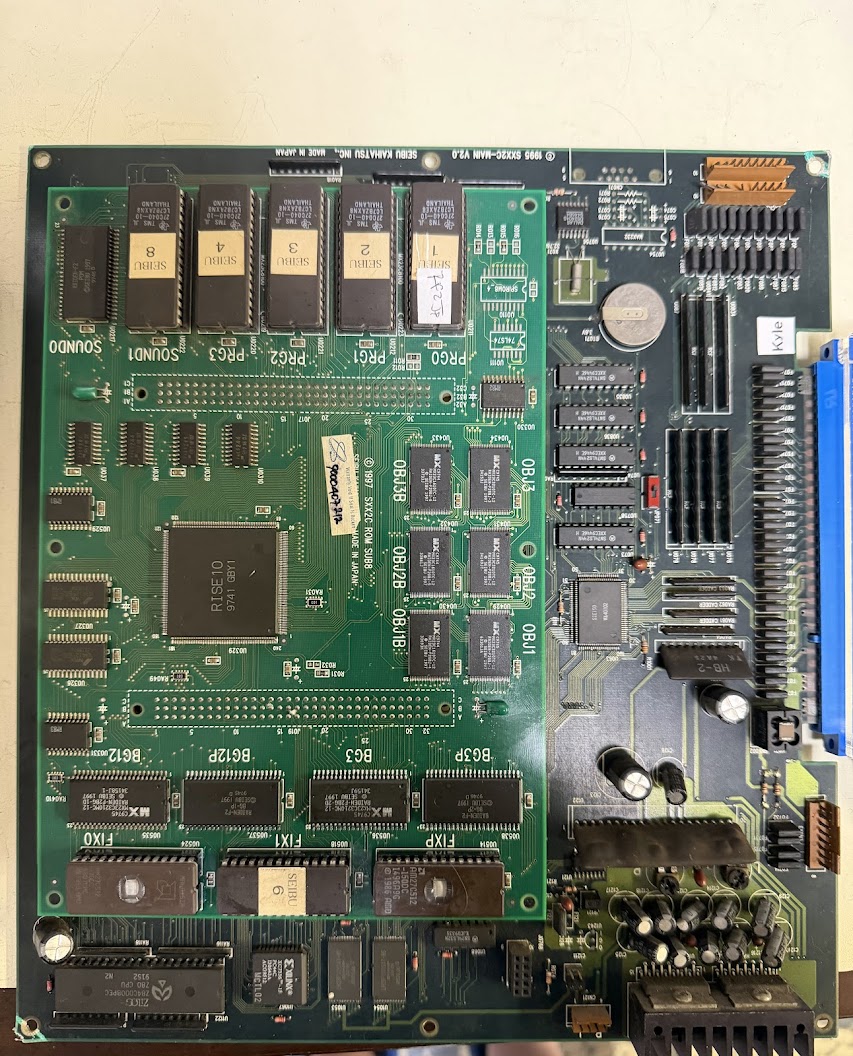
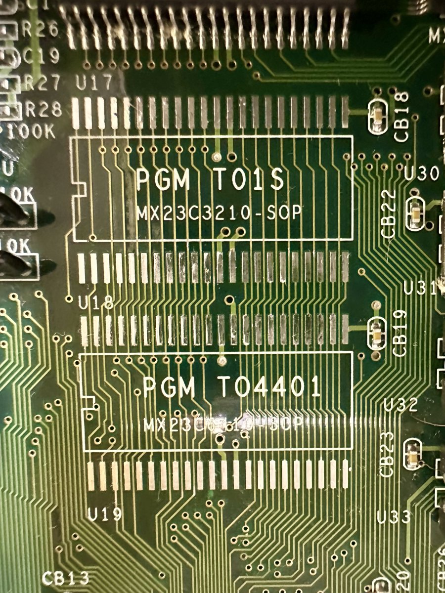
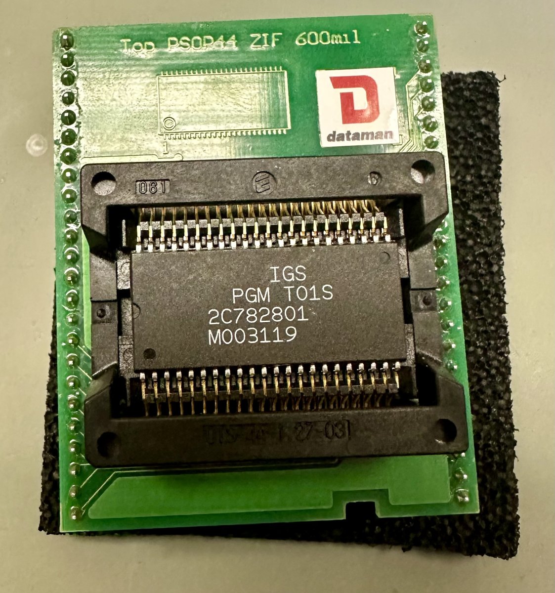
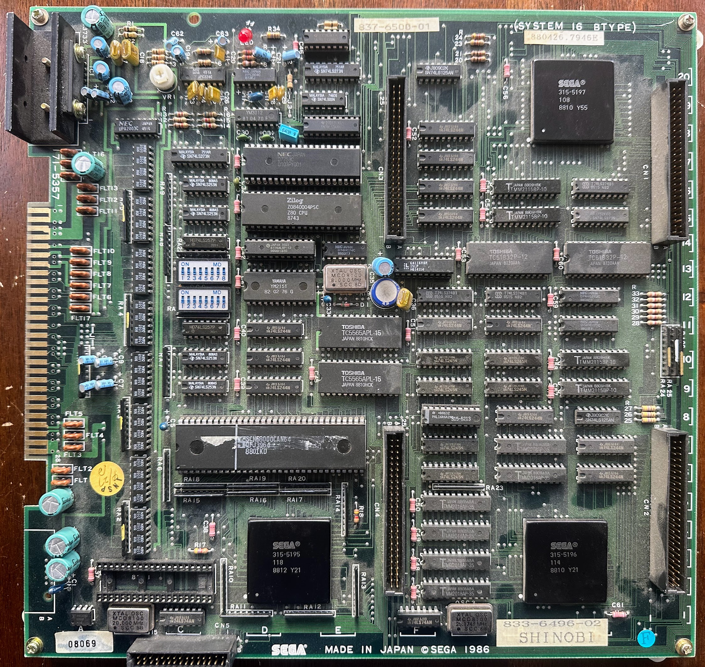
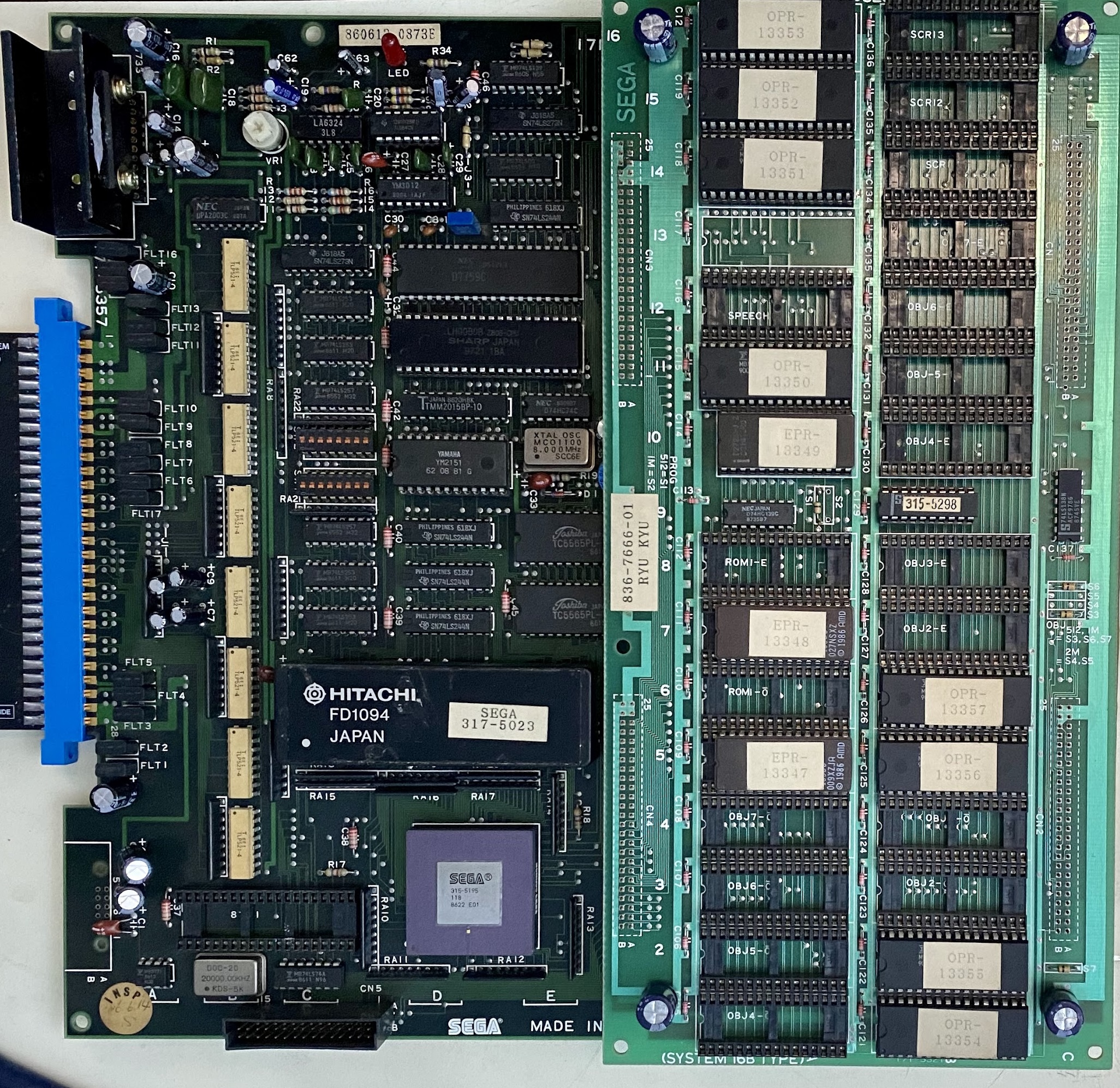
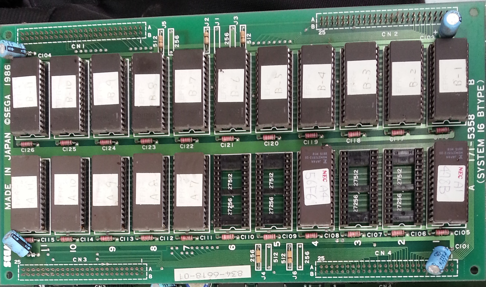
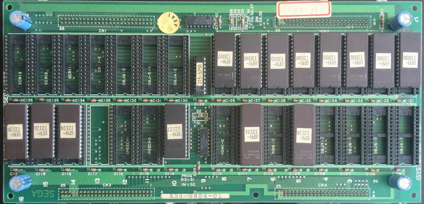
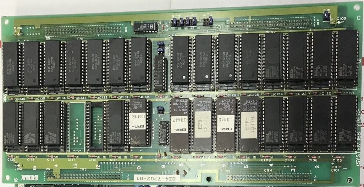
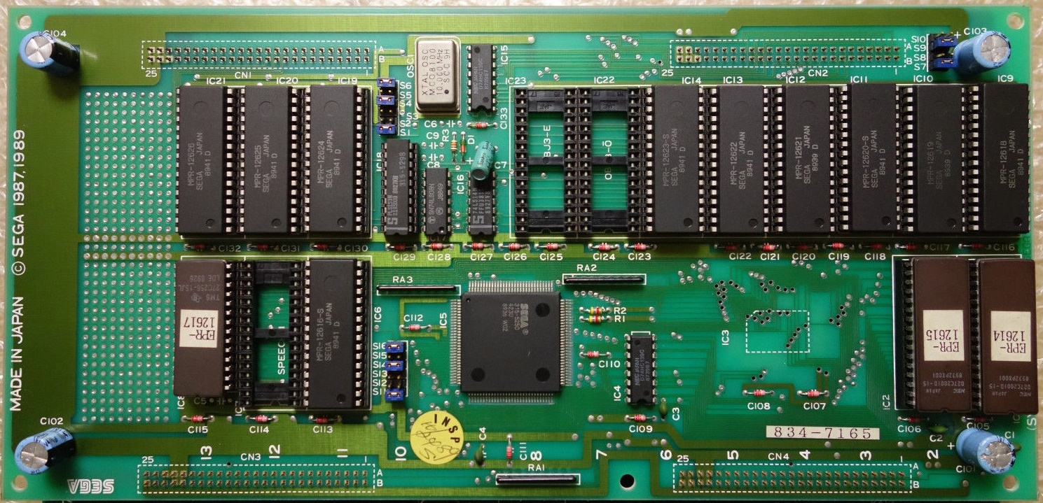
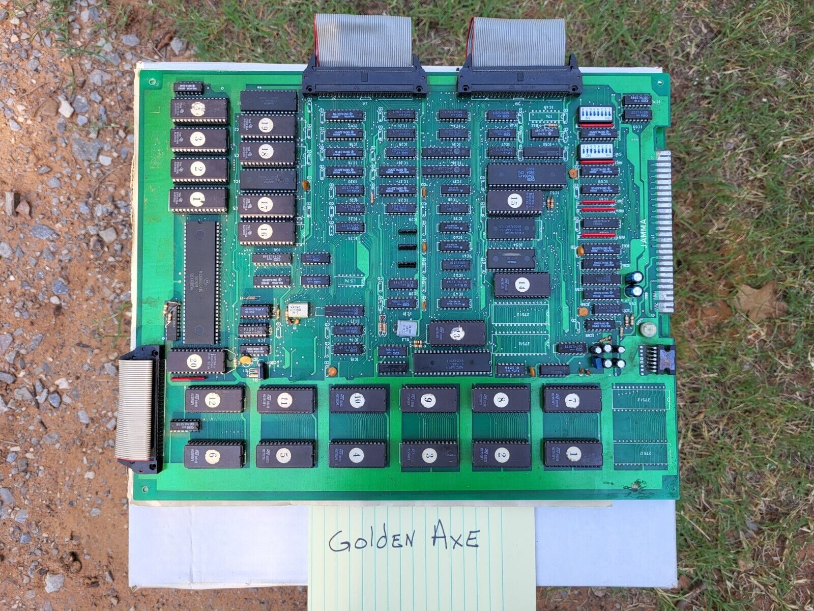
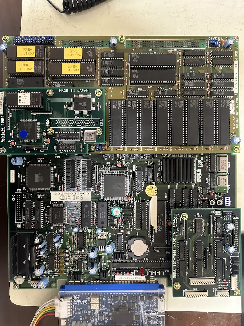
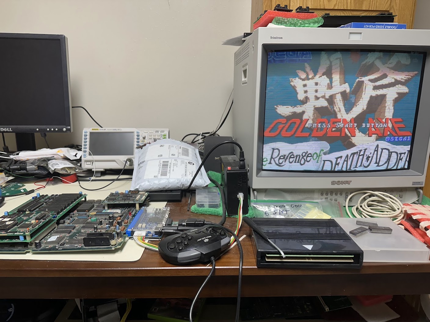
In for repair is a Sega Golden Axe II Revenge of Death Adder boardset. The board set consists of a large mainboard that handles all the logic processing, a daughterboard with the game data ROMs and another daughterboard that handles inputs for Player 3 and Player 4.

Although the boardset is in clean physical condition, it doesn’t boot up.

The first question with any Sega System 16, 18 or 32 game board that won’t boot up is “Has it suicided?” All three platforms used encrypted code on the CPU ROMs and a protection mechanism to decrypt the code before it runs on the Main CPU. If the protection mechanism fails then the Main CPU hangs waiting for code it can run. Sometimes the protection mechanism is battery-powered, and when the battery dies then the decryption mechanism permanently breaks – hence the term “suicide”.

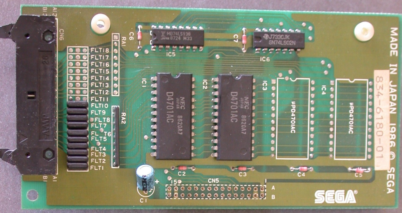
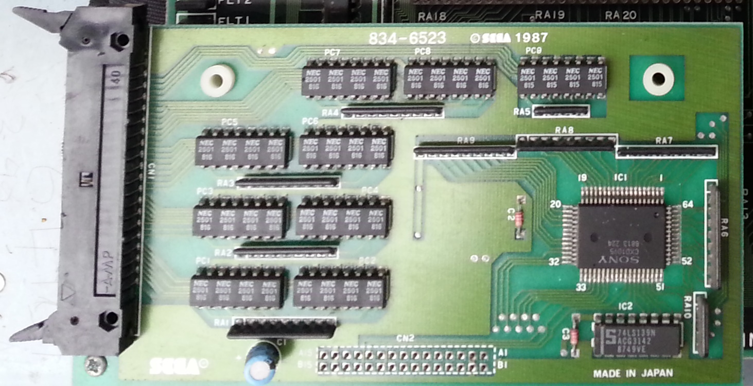
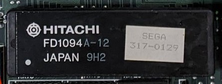
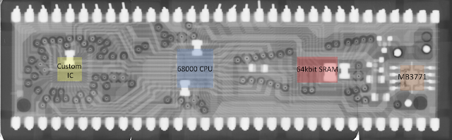
In the case of Golden Axe II, the protection mechanism is this small daughterboard sitting on top of the ROM board.

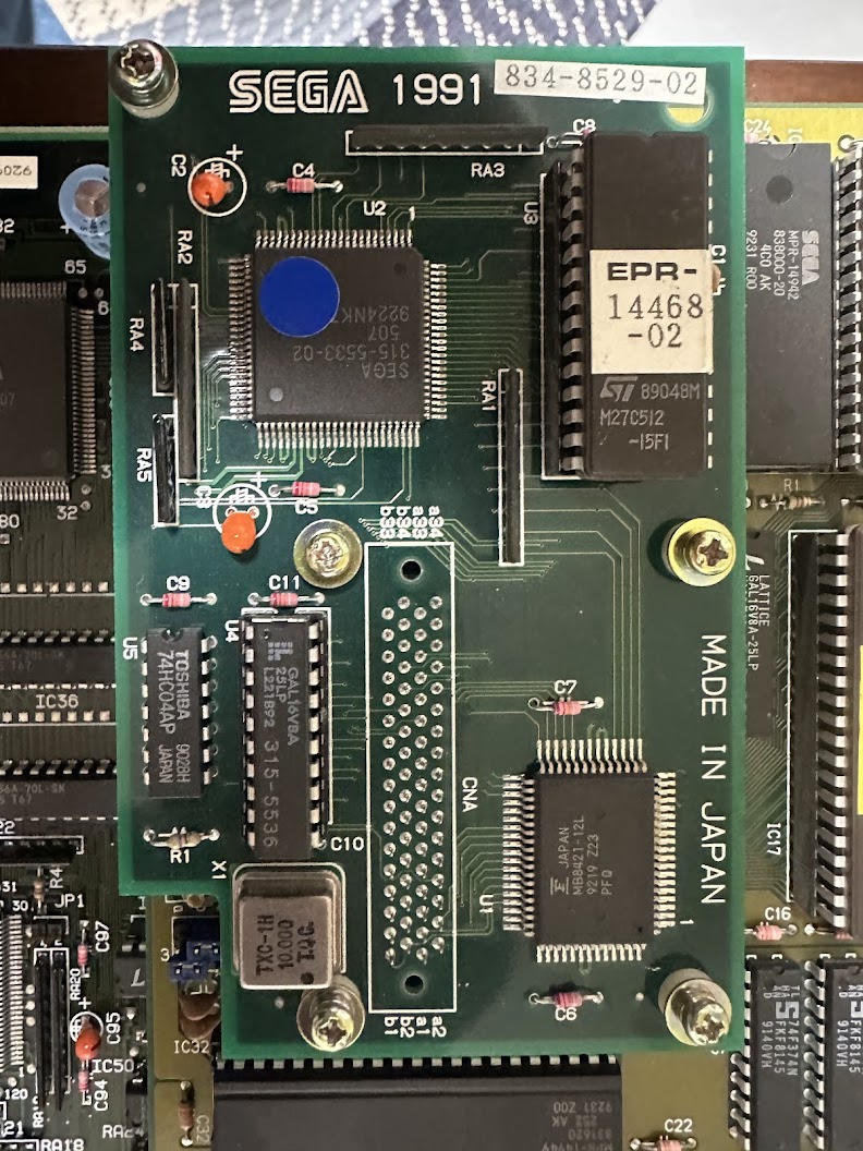
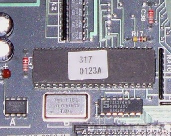
This protection board is a mini-computer by itself. The Sega 315-5533-02 is a relabeled NEC V25 CPU running at 10 mhz that executes its code from the single onboard EPROM and uses the Fujitsu RAM for processing the decryption algorithms. Here, it’s possible for either the onboard EPROM to become corrupted or the Fujitsu RAM to fail, resulting in the decryption CPU crashing and the Main CPU then hanging up waiting for incoming code it can run. At least there’s not a battery here to worry about…

Fortunately, I had a quick and easy method to determine if this Golden Axe II ROM board had suicided. I have my own fully-functional Golden Axe II board set, so I swapped the project’s ROM board over to my personal main board and powered up.

The game booted up and played perfectly. Therefore the ROM board hasn’t suicided and the problem is with the System 32 main board.

I hadn’t worked on a System 32 main board before, so I started performing some research. Specifically, I wanted to know:

  • Are schematics available for this hardware?
  • Are there repair logs of other technicians resolving similar issues with this hardware?

As far as schematics go, Nemesis has scanned and shared them. In order to aid SEO, I also mirrored them here. As far as repair logs go, The Guru has logs on several similar System 32 repairs. Here are some key discoveries I made from Guru’s writeups about Sega System 32 hardware when the main board doesn’t boot up:

  • Reset signals originate at the TTL logic chips located at IC11 and IC12.
  • Clock signals originate at the two oscillators at the bottom-middle of the board and are distributed around the board by a handful of TTL logic chips (IC23, IC24, IC34, IC39, IC52, IC53).
  • The game will not boot if the NEC V60 Main CPU, Zilog Z80 Sound CPU or 315-5296 custom are nonfunctional.

Time to dig in. I started with checking the Reset signals. The Main CPU, Sound CPU, and some of the other components on the board need to be Reset when the board starts up. There is also a “watchdog” circuit which will trigger the Reset lines and reboot the game if the watchdog detects that the game has frozen. On a logic probe or oscilloscope, the Reset pin on a CPU should initially read High at powerup, go Low briefly as the Reset circuit triggers, then return to High.

I probed the NEC V60 Main CPU Pin 52, Z80 Sound CPU Pin 26 and the outputs on the TTL logic chips at IC11 and IC12. They all showed that the Reset circuit was operating as expected.

Next, I investigated the Clock signals. Think of the Clock as a “heartbeat” that drives the processing logic on the board and keeps everything in sync. Without appropriate Clock signals, the board won’t run.

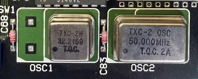
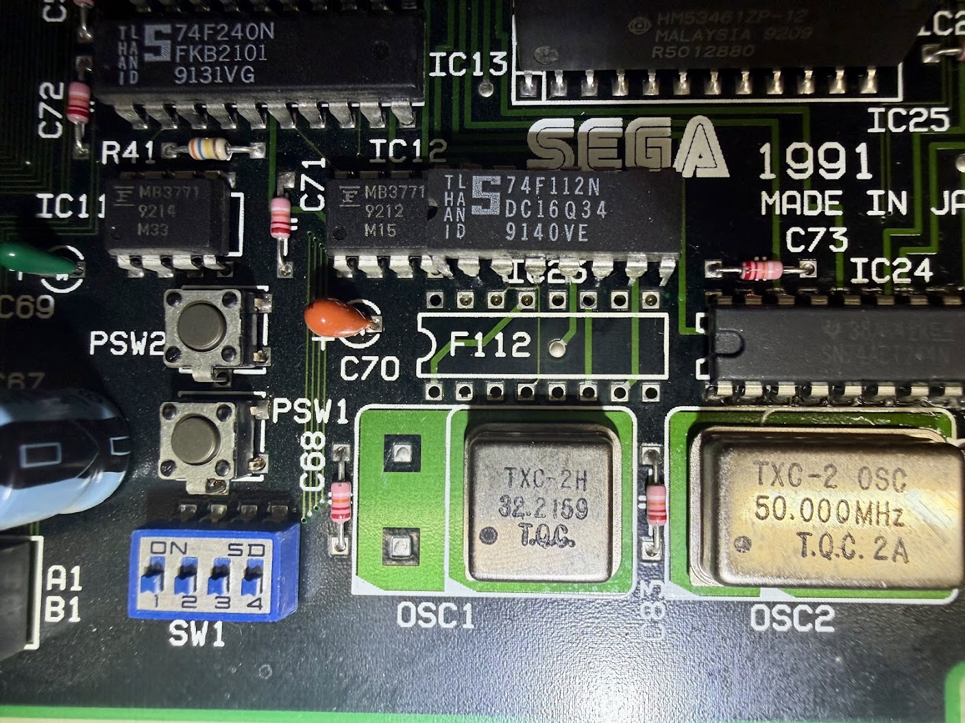
Clock signals originate from crystal oscillators. The Sega System 32 main board has two of them located in the bottom middle of the board – a 32.2169 mhz clock and a 50 mhz clock.

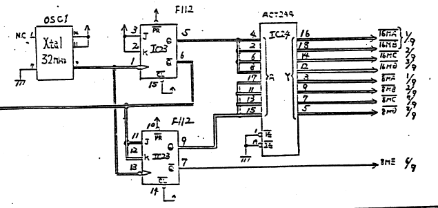
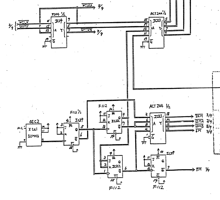
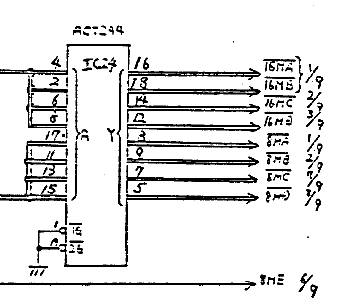
These clock signals are then distributed around the board and subdivided to lower speeds as needed by a variety of TTL logic chips. Here is the appropriate clock distribution circuits from the schematics.

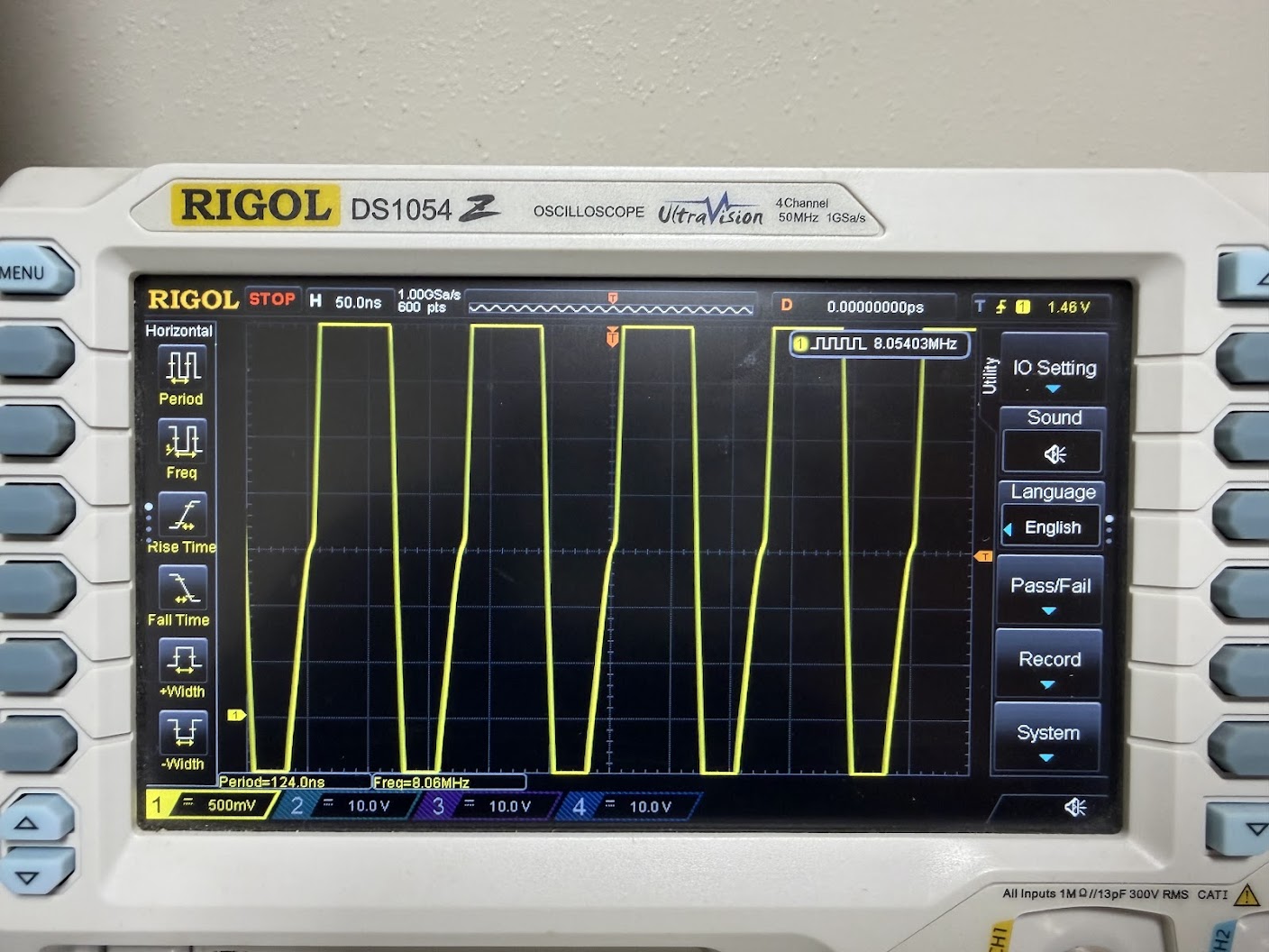
Many components need a clock signal, but I started by checking the clock input pin on the NEC V60 Main CPU first. The V60 Clock Input pin is Pin 13 and it showed the expected 16 mhz clock signal.

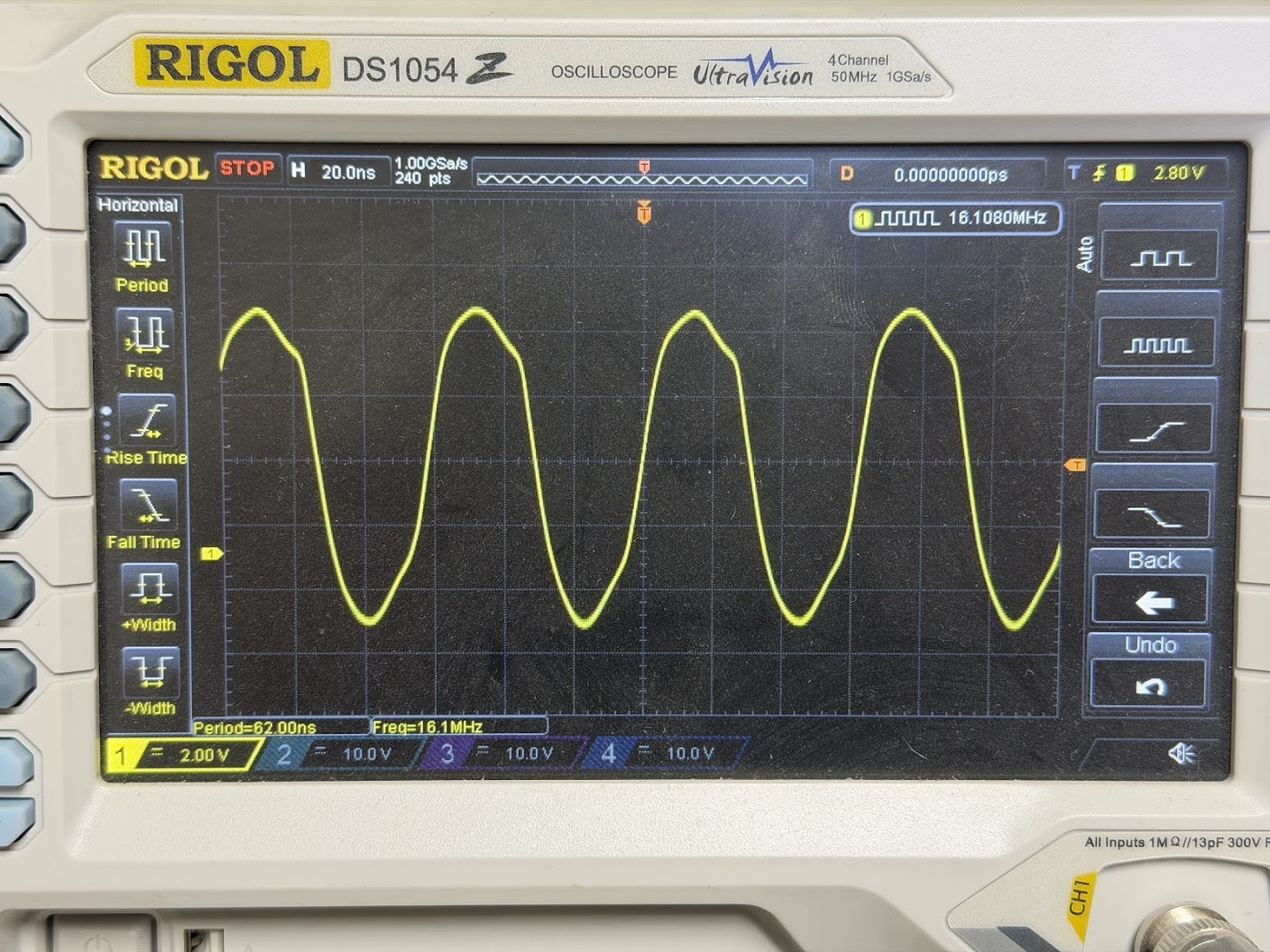
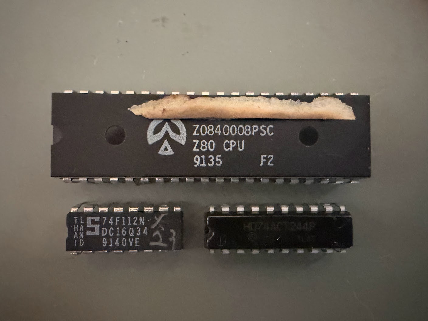
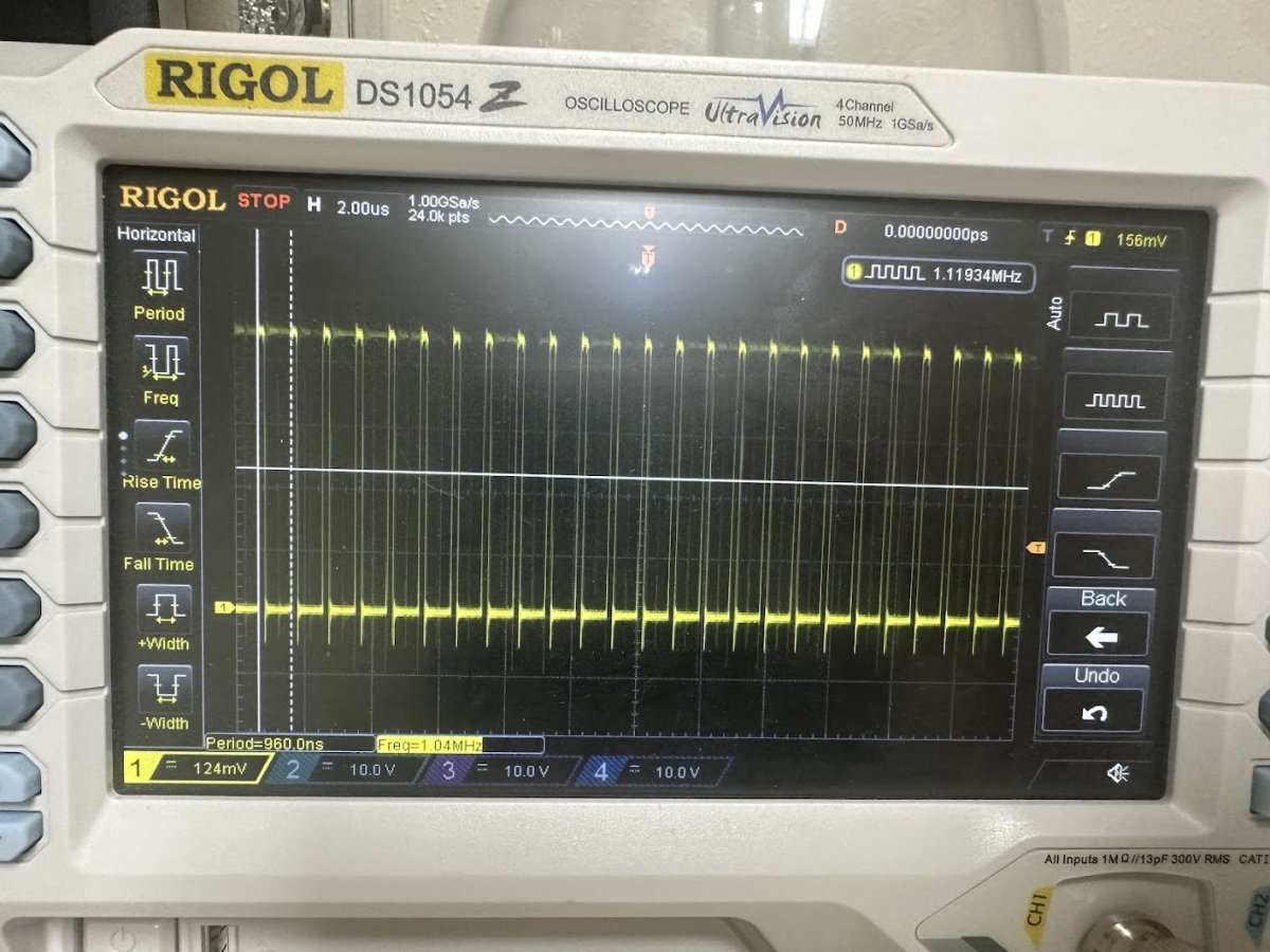
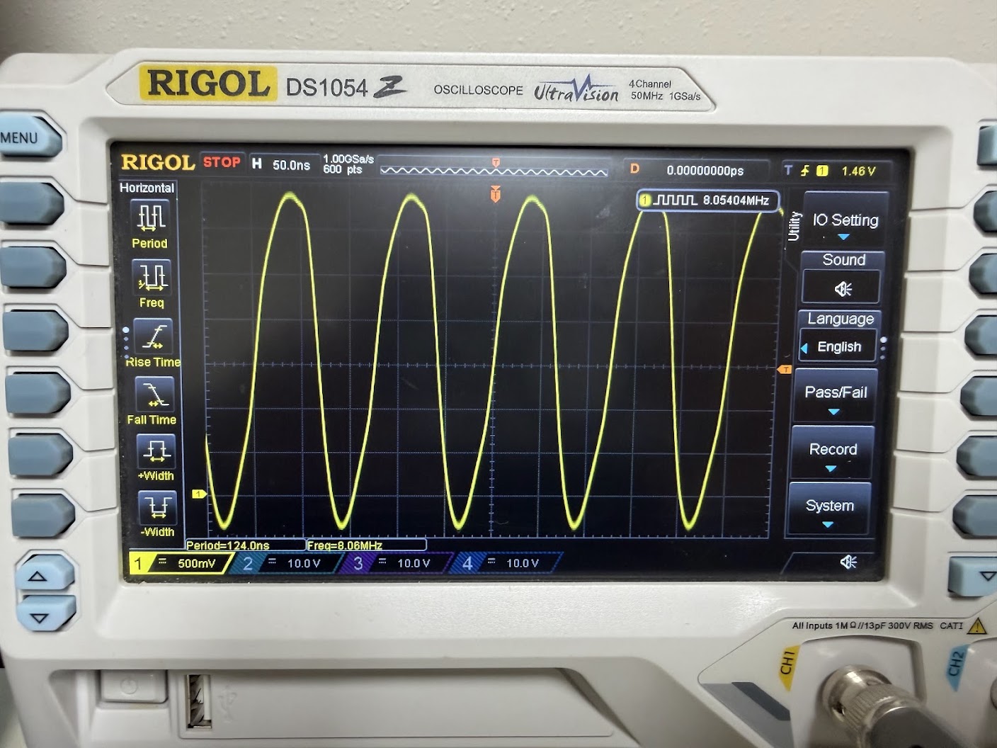
The Z80 Sound CPU clock input is Pin 6 and its signal looked awful.

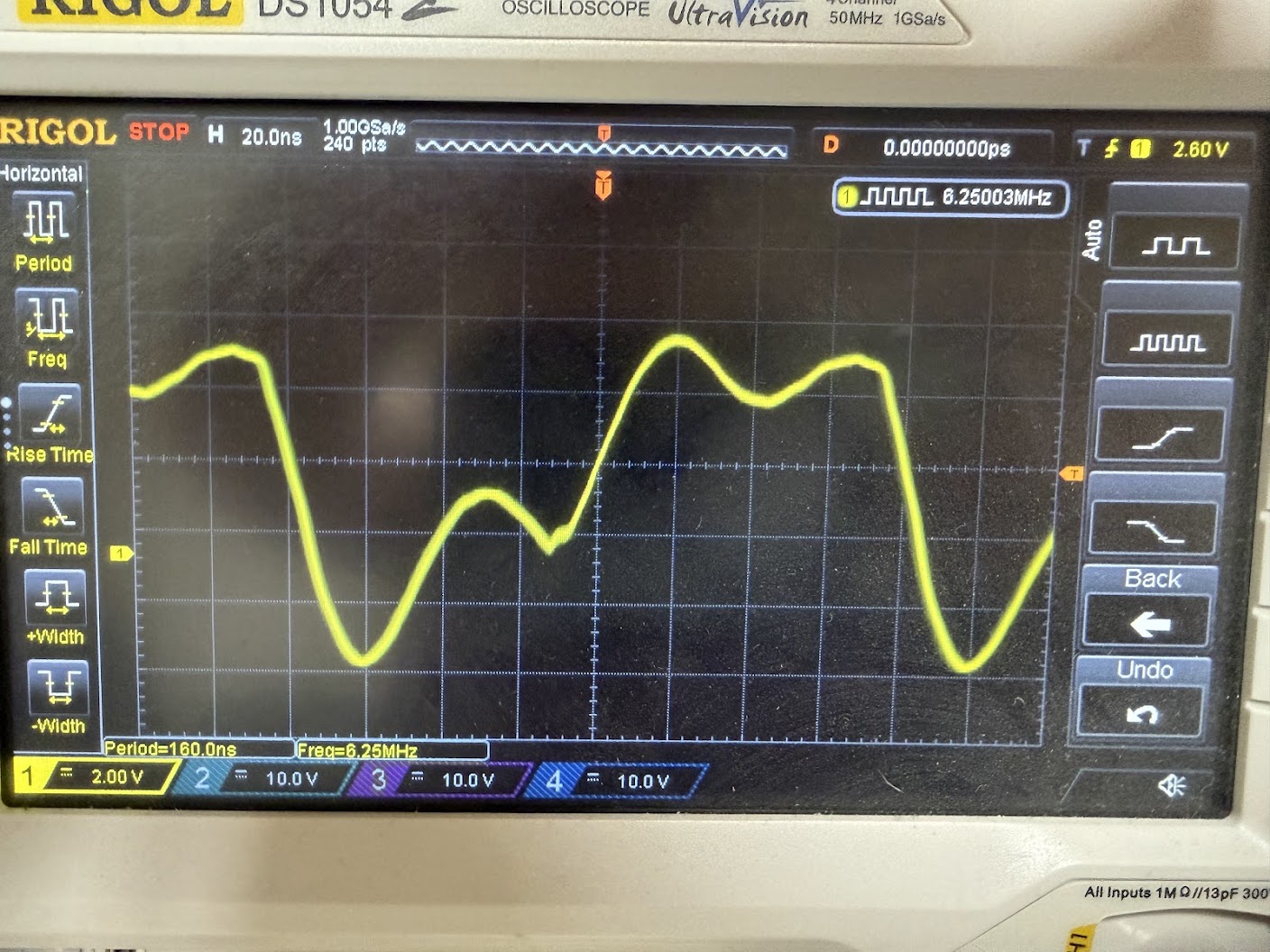
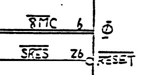
Time to check the TTL logic chips that feed the clock signal to the Z80. The Z80 clock signal line is labeled “8MC” on the schematics.

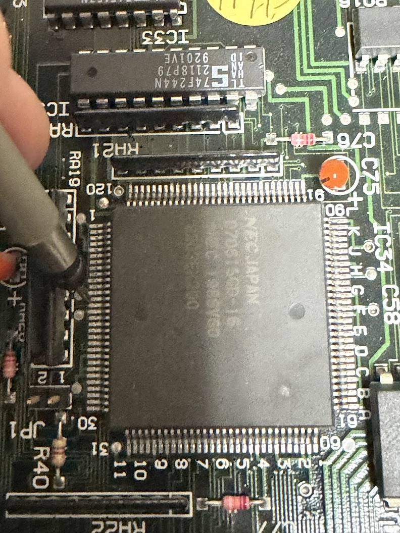
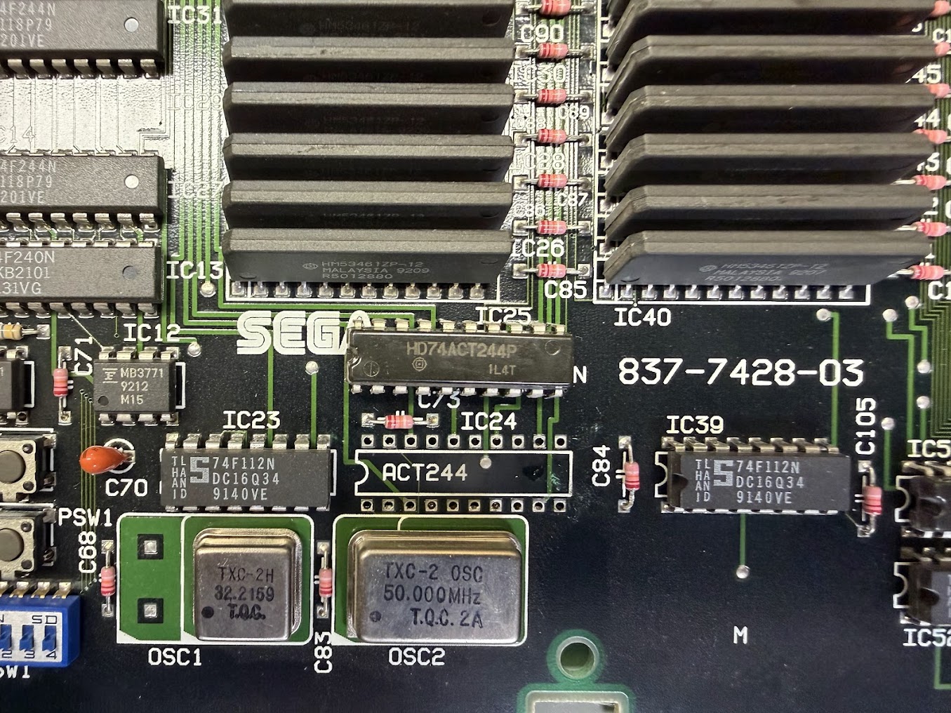
And the schematics show that 8MC is output from Pin 7 on a 74LSACT244 TTL chip located at IC24.

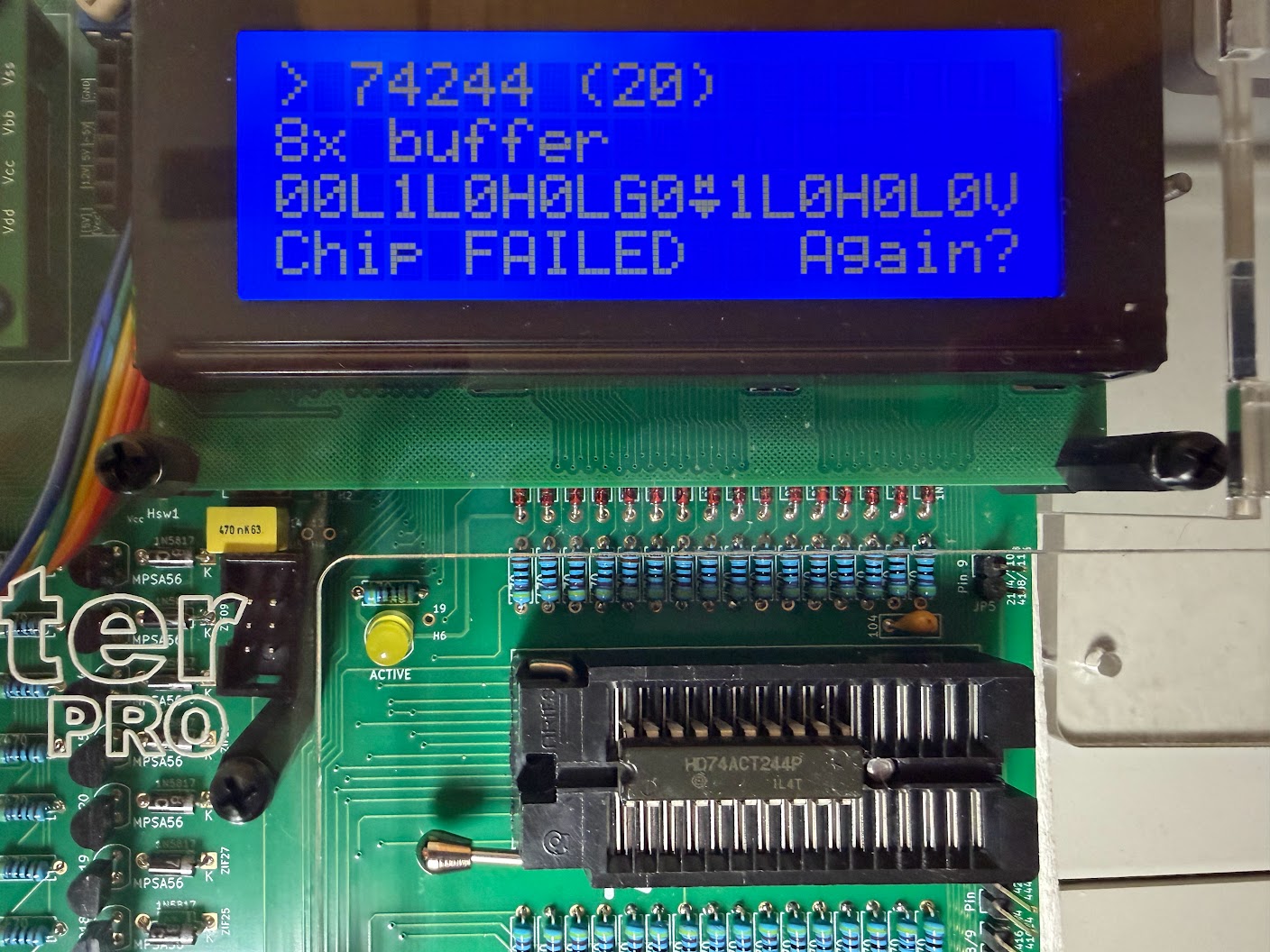
I desoldered IC24 from the board and it tested bad out-of-circuit in my logic chip tester.

Since clock signals are driven at a high speed, a standard 74LS244 replacement part won’t suffice. A standard 74LS244 can handle 10 – 15 ns signal switching. The ACT designation on both the schematics and board means that a faster ACT series chip capable of 1 -2 ns signal switching is needed. I had to order some in and for them to arrive.

Unfortunately, the replacement part didn’t fix the board – it still hung with a black screen at boot. I started probing around the other TTL parts in the clock distribution circuits, when to my surprise the board suddenly sprung to life!

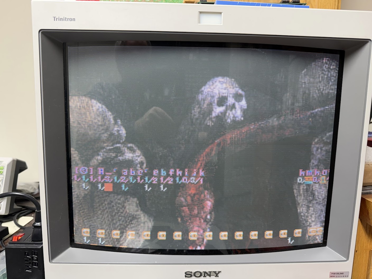
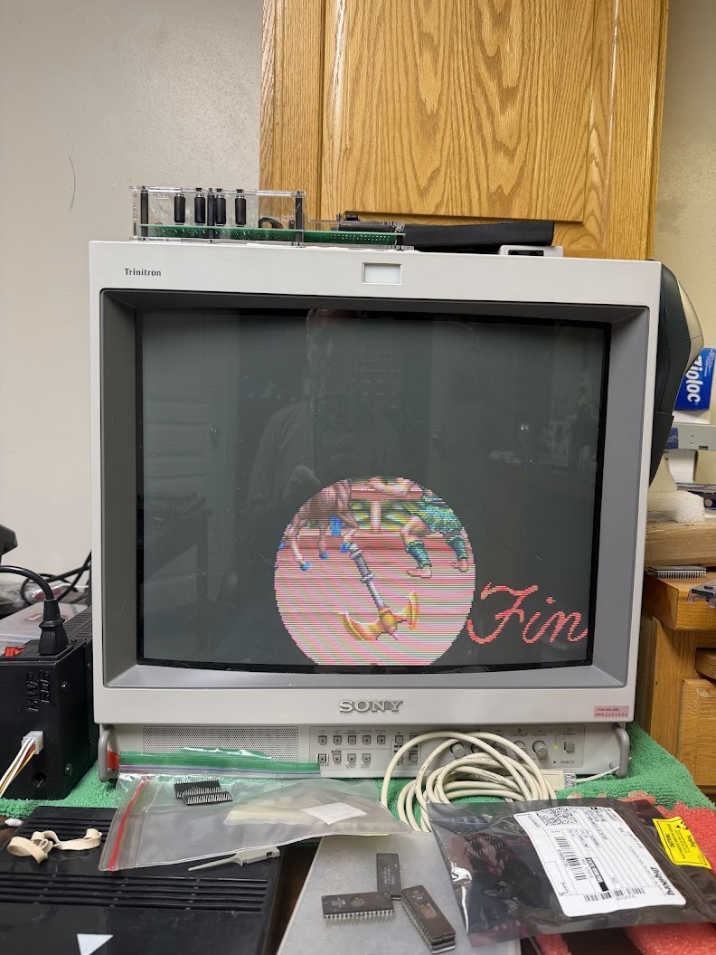
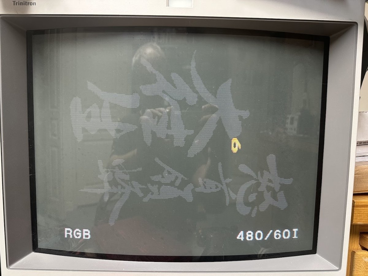
Sure, the sprites were garbled and there wasn’t any sound, but I was still pleased to see signs of life. This definitely hints at more problems in the clock distribution circuits. I found that probing IC23 is what would jumpstart the board, so I desoldered that part from the board, and sure enough it tested bad out of circuit.

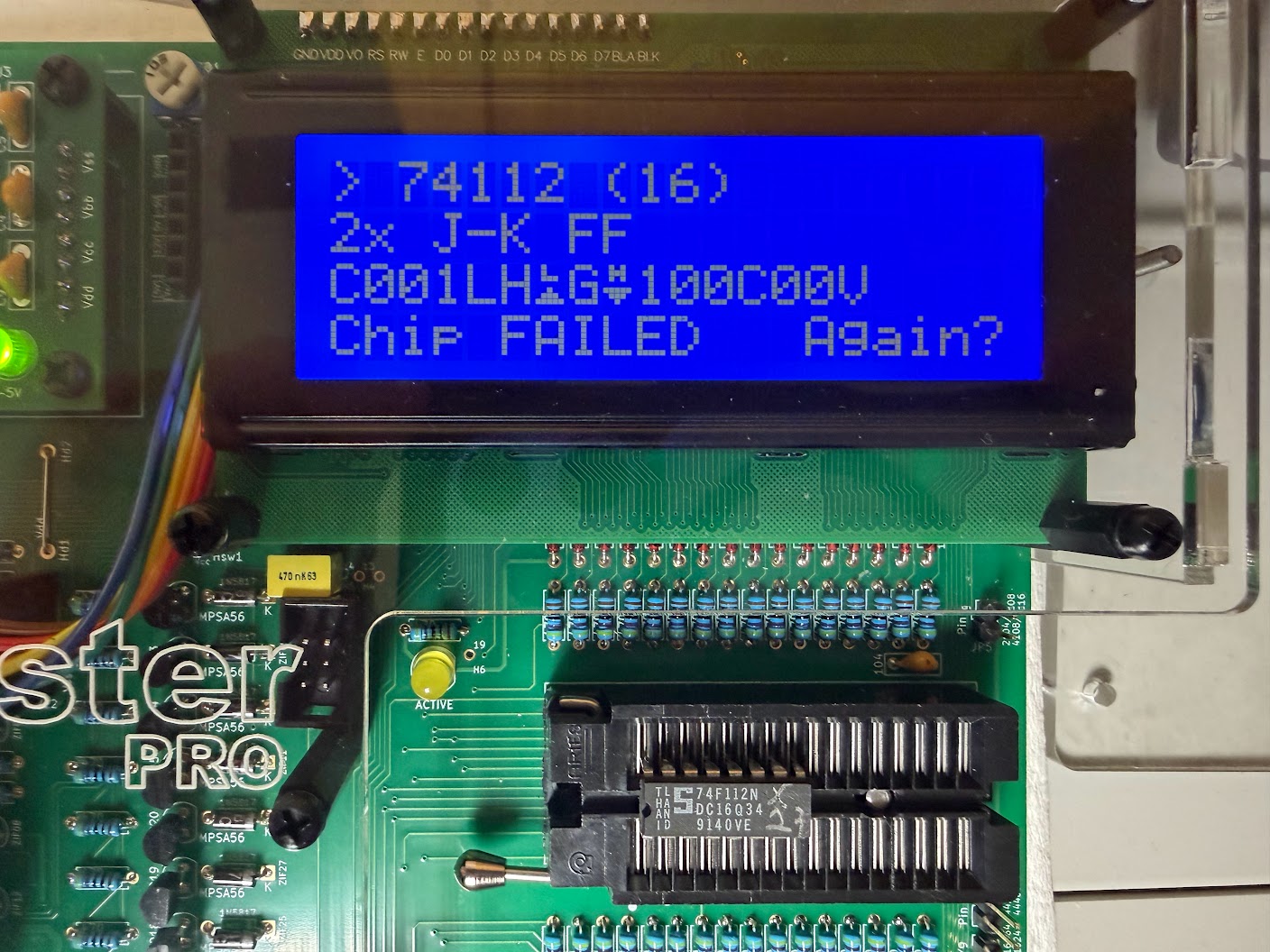
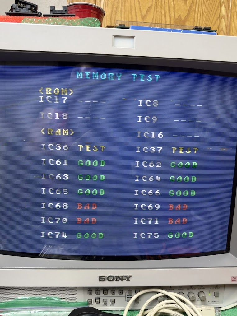
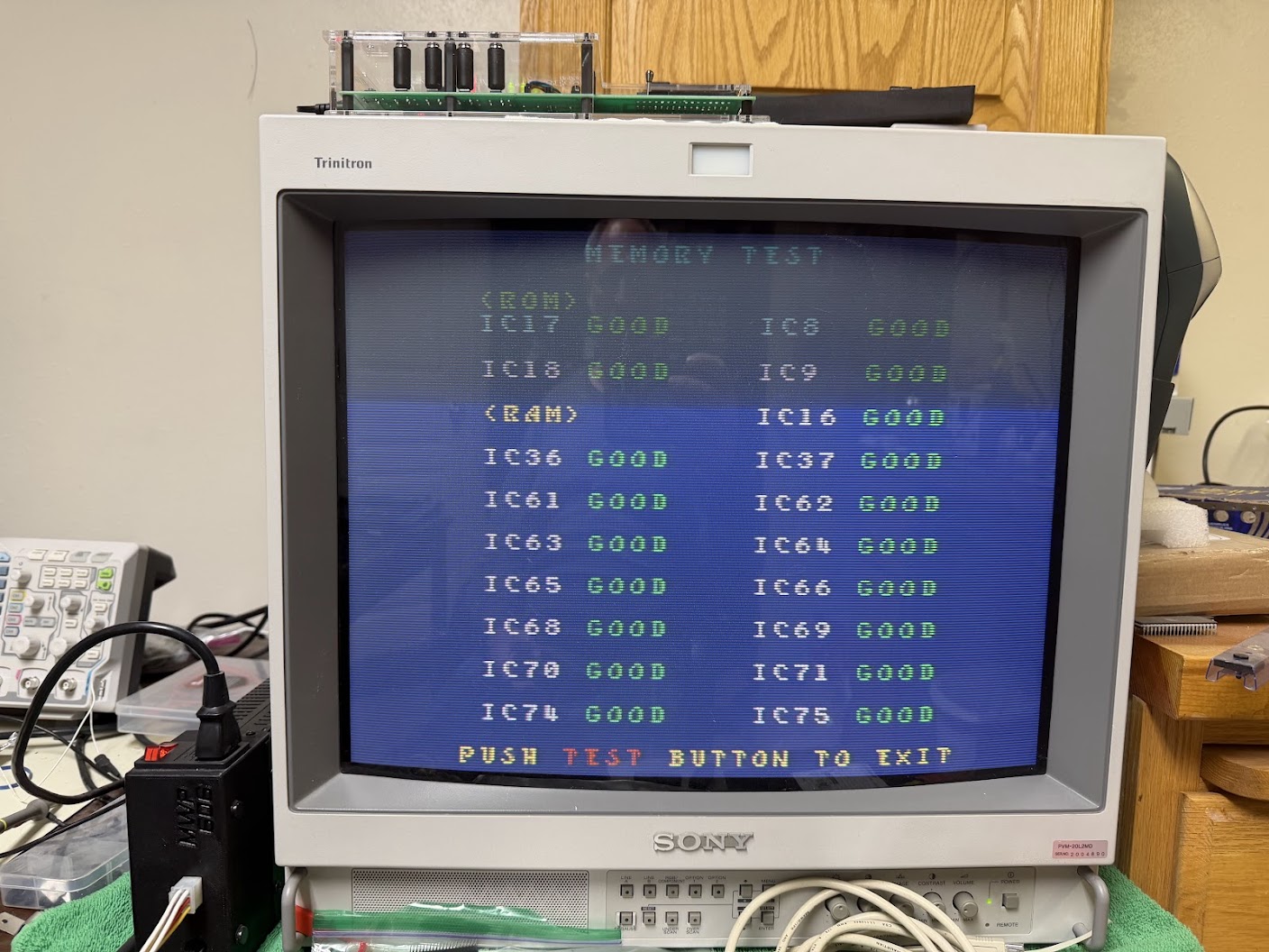
This part is a 74F112N and I had planned ahead and ordered replacements for these in at the same time as the ACT244s, so I was able to swap a fresh part in right away. However, it still didn’t completely solve the problem. The board would now boot up on its own with clean graphics, but not consistently. The sound also didn’t work, and the game would freeze up often. The self-diagnostic routine in the Service Menu marked four components as faulty and then froze when testing the ROMs.

Since the sound wasn’t working, I decided to check the Z80 Sound CPU in detail for proper operation next.

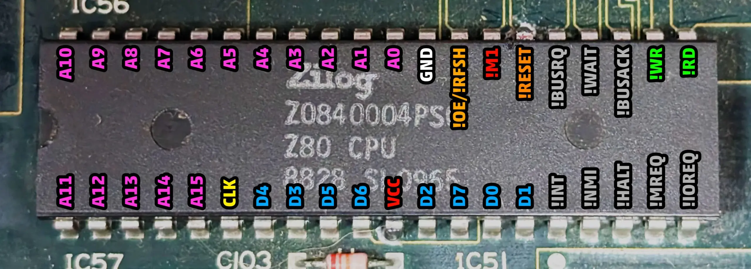
In addition to the Clock and Reset signals I mentioned earlier, there is also the HALT signal on Pin 18 that will go High only if the Z80 software program triggers it to stop. It probed Low as expected.

Pin 27 is M1 and it starts High and toggles Low when fetching an opcode from memory at the beginning of every machine instruction in the software program. The M1 signal on this Z80 probed as holding High continually so the CPU was not processing instructions – very suspicious.

Next, I checked the WAIT signal on Pin 24. If it is holding Low then another component on the board is triggering the Z80 CPU to stop. It probed as holding High, so nothing else was triggering the Z80 to wait.

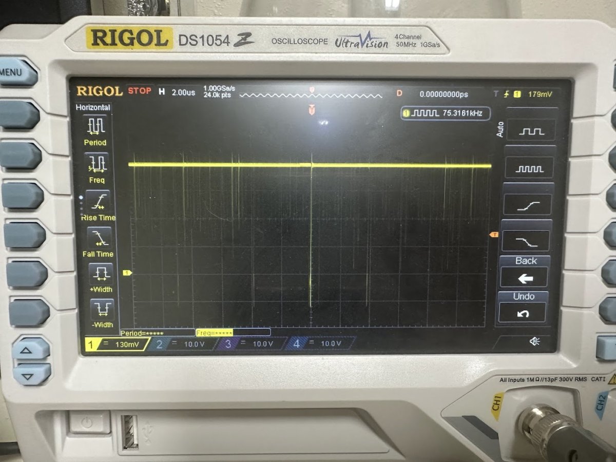
Then, I checked the BUSRQ (Bus Request) signal on Pin 25. If it reads Low, that means that another peripheral on the board (such as a DMA controller) has asked the Z80 to release the bus so shared resources (such as memory) can be accessed. The Z80 triggers the BUSAK (Bus Acknowledge) signal after it’s released the bus so that the requesting peripheral knows it can proceed with its operations. The requesting peripheral would then set BUSRQ back to High again when it completed its work and was ready for the Z80 to take back the bus and resume operation. In this case, the BUSRQ signal showed High briefly at power on, then went Low and held there. This meant that the Z80 was receiving a signal to release the bus but then never received a signal to “wake back up” again. Suspicious!

Finally, I checked the BUSAK signal on Pin 23 and finally found the smoking gun. BUSAK is only supposed to trigger after a BUSRQ signal, but on this Z80 the BUSAK was triggering continuously – at exactly the same frequency as the Z80’s 8 mhz Clock signal no less!

This confirmed that the Z80 Sound CPU had failed internally in such a way that the BUSAK line was “echoing” the Clock signal. That was likely confusing all the other components on the board that tied to it!

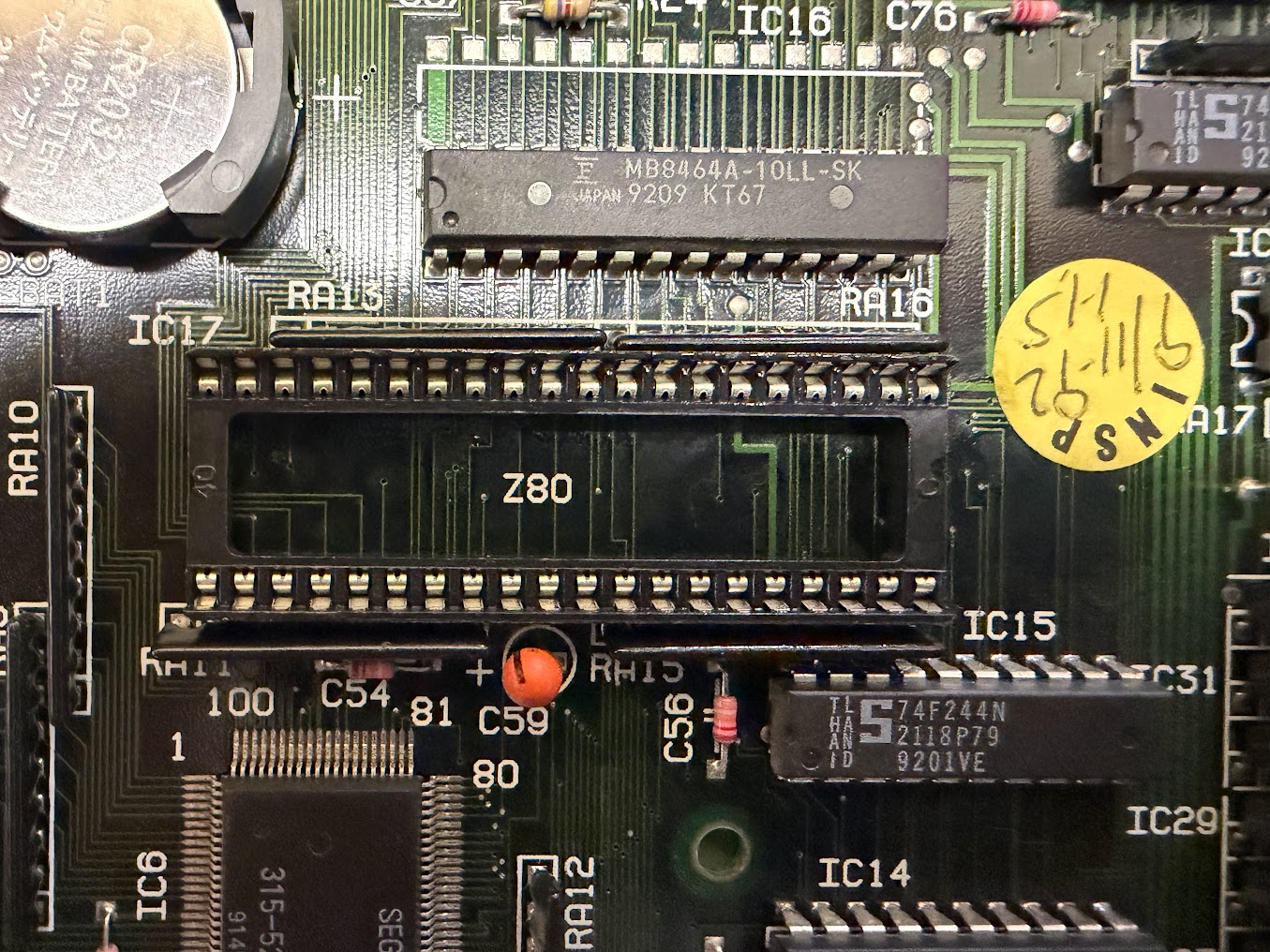
I desoldered the Z80 CPU, installed a 40 pin socket, and swapped in a replacement 8 mhz Z80 CPU.

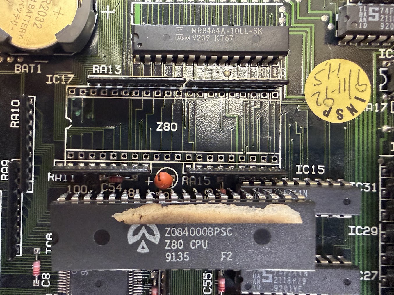
Happily this time when powering on, the board functioned perfectly! Sound was present, the game didn’t freeze up, and the self-diagnostics passed with flying colors!

For good measure, I played through the entire game successfully, and left the game running overnight. There were no freezes and the game continued working perfectly. A successful repair!

Seibu Kaihatsu SPI & Raiden Fighters 2

 PCB Repair Logs, Repair Logs  Comments Off on Seibu Kaihatsu SPI & Raiden Fighters 2
Jan 142026
 

In for repair is a Seibu Kaihatsu SPI mainboard (V2.0 Revision) and a Raiden Fighters 2 game cartridge.

The SPI mainboard wouldn’t boot – on powerup, it would display a generic “Checksum Error” message.

This is a common problem with the SPI platform. The SPI mainboard and game carts are region coded. If the cart region doesn’t match the mainboard region then you’ll see this error. Additionally, when a game cartridge is accepted, portions of it are flashed to chips on the mainboard. If something goes wrong during the flash process, the mainboard’s region code can be lost, causing it to no longer work with any game.

Happily, Trap15 created a tool called SPI Revive that can be used to write a new region code onto an SPI mainboard. I connected my SPI Revive cartridge, and it shows that the region code for this board is “zero” meaning that it was indeed bricked. I told SPI Revive to write the Japan region code to the board, which it did successfully.

After reconnecting the Raiden Fighters 2 cart, the board started up successfully, flashed itself to the mainboard successfully, and then prompted to restart. After restarting, the game boots up and runs fine, but with “jailbar” lines of corruption running through the sprites.

This is another common issue with game cartridges on this platform. There are several SMD ROMs and a large SMD custom chip. Not much solder was used at the factory and over time, some of the chip legs can detach from their solder pads, breaking the connection.

One way to test for this problem is to press on various chips on the PCB and watch the screen to see if the graphics change. I used a plastic spudger and noticed the jail bars would flicker when I used it to press on ROM chips in the OBJ section. I reflowed the solder on them.

Afterward, the game boots up and runs fine with crisp, clear graphics and sound. The final touch is applying reflective stickers to cover the exposed windows on the two EPROMs missing them on the game cart. A successful repair!

DoDonPachi Dai-Ou-Jou PCB Repair

 PCB Repair Logs, Repair Logs  Comments Off on DoDonPachi Dai-Ou-Jou PCB Repair
Sep 162024
 

In for repair is a DoDonPachi Dai-Ou-Jou (DDP DOJ) arcade board by Cave. It boots up fine but the backgrounds and most of the text are missing.

DDP DOJ runs on the IGS Poly Game Master (PGM) hardware. Although DDP DOJ was never officially released as a PGM cartridge, the game was easily dumped from the original stand-alone boards and can then be loaded onto a PGM cartridge.

According to the MAME driver for the PGM, two ROMs are involved in drawing the backgrounds – a BIOS ROM and an asset ROM.

In MAME, I overwrote the “pgm_t01s.rom” BIOS ROM file with all “FF” but the game still booted up and played fine. Overwriting the “cave_t04401w064.u19” file with all “FF” replicated the real board’s behavior in MAME.

This implied that the mask ROM located at U19 was only reading out “FF”. Probing the address and data lines of that mask ROM on the running board confirmed it – the Address lines would signal properly but the Data lines pretty much always read High.

I desoldered both the U18 BIOS ROM and U19 asset ROM chip and attempted to dump them both as a 29F1610 flash chip since that part has the same pinout. The 29F1610 is a 16 Mbit part that matches the 16 Mbit BIOS but is only one-quarter of the 64 Mbit total stored in the background asset ROM. But even with only one-quarter of the background ROM dumped I’d be able to see if data is reading out of the ROM properly.

The BIOS ROM successfully reads out data but the background asset ROM only reads out FF – looks like the background ROM is toast.

Now for a dilemma – what to do about replacing a dead DDP DOJ background asset mask ROM? The original part is a MX23C3210 mask ROM. There is not a programmable off-the-shelf part with 64 Mbit capacity and the same 5V voltage that the PGM hardware uses that also matches the pinout and footprint of the original mask ROM.

I did prototype a solution that I will describe at the end of this post, but for now I’ll skip to the end of the repair and say that the owner of this board sourced a dead donor PCB of the same game. I was able to successfully transplant the BIOS and art asset mask ROMs from the donor to this PCB and it worked correctly afterwards – a successful repair.

Stepping back to earlier though, while the owner searched for a parts donor, I reached out to colleagues on both the Arcade Projects forums and on Discord for advice for replacing the dead 64 Mbit asset mask ROM. One consideration was to use four 29F1610 16 Mbit flash chips with a 74LS08 TTL chip to drive the Chip Enable lines. A second consideration was to use two 27C322 32Mbit EPROMs – that’s what the PGM cartridge conversions of DDP DOJ use. The drawback to both of these approaches is that the substitute chips would take up a lot more physical space than the original mask ROM so attaching them to the board would be challenging.

A third consideration that I proceeded to prototype with was to adapt an Intel DA28F640 flash chip. The DA28F640 is 64 MBit capacity, 5.0V compatible and programmable but it has a completely different pinout and footprint. I’d never created my own circuit board before, and this seemed like a great opportunity to learn KiCad. Over a few evenings, I referenced data sheets, took measurements, and produced an adapter board.

By the time the production adapter boards arrived, the game had already been fixed with the mask ROM from a donor PCB so my adapter is untested for now. Hopefully I’ll get a chance to try it with a different repair.

Here are the data sheets of the parts involved in this repair, along with the KiCad project files for the flash adapter PCB. If you use this adapter for a repair, please let me know if it works for you!

MX23C3210 mask ROM datasheet
Intel 28F640 pin assignments datasheet
Intel physical footprint datasheet
Flash Footprint Adapter KiCad files (Currently Untested)

Seibu Kaihatsu SPI

 Encyclopedia  Comments Off on Seibu Kaihatsu SPI
Apr 182024
 
Last Updated: 4/18/2024
Article Credit: ShootTheCore, Ikotsu, rtw, Trap15, ekorz, twistedsymphony, channelmaniac

The Seibu Kaihatsu SPI platform was offered in two configurations:

  • Two Board – Main Board and cartridge ROM Board
    • Region locked: Main Board must match country of cartridge ROM Board. This protection can be bypassed – see “Protection Mechanisms” below.
    • Optional Stereo audio.
  • Single Board
    • Only runs the one game that was loaded onto it at the factory.
    • Offered with two different audio setups- Yamaha YM-271-F or dual OKI MSM6295
    • Mono audio only.

This article will address the two configurations separately.

Two-Board Configuration: Main Board

The SPI main board contains all the processing logic to run the game. It was released with two revisions, both of which can run the same ROM game cartridges. The marking on the board for each revision is:

  • (C)1995 SXX2C-MAIN V2.0
  • (C)1998 SXX2D-MAIN V2.1

Stereo sound output is available on the two-board SPI configuration through the CN1 connection header. Everten sells a nice add-on board that adapts the CN1 header to standard RCA stereo audio ports.
https://shewfly.com/products/seibu-kaihatsu-spi-stereo-board-by-everten
https://www.candycabclub.com/product/everten_spi

The video and audio quality is said to be better with the SXX2C-MAIN V2.0 revision.
Source: https://shmups.system11.org/viewtopic.php?t=43308

The SPI system has onboard flash memory used for both region lockout and to store part of the game. The V2.0 board restricts write access to the flash memory by a jumper labeled JP072. The V2.1 board does not have any flash write access restriction jumper.

When swapping game cartridges, you will need to change the jumper (V2.0 only), install the new cart, power on, wait for the game to write to the flash memory (the message “NOW UPDATING. PLEASE WAIT A MOMENT.” will be displayed), power down and flip the jumper back (V2.0 only). Even after flashing, the ROM cartridge must stay attached for the game to operate.

Notable ICs

ICFunctionPCB Label
AM386DX/DXL-25 – OR –
Intel NG80386DX25
25.0 Mhz Main CPUU0169
Zilog Z84C0008PEC7.15909 Mhz Audio CPUU1122
Yamaha YM271-FAudio Processor and Flash AccessU1020
Yamaha YAC513-MAudio DACU1068
Intel E28F008SA – OR –
Sharp LH28F008
8 MBit FlashROMU1053, U1054
SEI400Graphics RenderingU048
SEI600Graphics RenderingU0154

Two Board Configuration – ROM Cartridge Board

Cartridge boards include DIP socket EPROMs, SMD mask ROMs, SRAM and a custom decryption IC – see Protection Mechanisms below. It is not possible to reliably convert one SPI game cart to another at this time, although it is possible to upgrade the same game to a different version (ie Viper Phase One to Viper Phase One NV).

ROM Board model numbers

  • SXX2C ROM SUB
  • SXX2C ROM SUB2
  • SXX2C ROM SUB4
  • SXX2C ROM SUB8
  • SXX2C ROM SUB10

Common Issues and Quirks

CHECKSUM ERROR or HARDWARE ERROR (credit: rtw & Trap15 and channelmaniac)

The two-board SPI platform stores part of the game inside onboard flash storage. The flash storage is also initialized from the factory with a country code. If the country code stored in the first byte of u1053 flash on the mainboard does not match the country code stored in the last byte of the PRG0 EPROM on the ROM cart then you will see the message CHECKSUM ERROR XXXX or HARDWARE ERROR XXXX during the flash process where XX is a two or four digit error code.

It is possible to desolder the u1053 flash chip from the main board to reprogram it with a new code. A list of the country codes is in the opening comments of the MAME driver.

Alternatively, Trap15 developed a software solution named SPI Revive that can rewrite the country code on the mainboard by swapping the PRG0 EPROM on a Raiden Fighters or Raiden Fighters 2 cart. If SPI Revive is unable to change the country code then the u1053 flash chip should be replaced.

SPI Revive: https://bitbucket.org/trap15/spi_revive/src/master/

Source: https://shmups.system11.org/viewtopic.php?t=62636

There have also been cases where the flash chips are holding the correct country code data but the board isn’t reading that data correctly. The Yamaha YM271-F sound chip controls access to the flash storage, so check the connections and traces on it.

Reflowing the solder on all of the large SMD ICs is recommended for HARDWARE ERROR and CHECKSUM ERROR messages if the earlier methods of writing the country code do not resolve the problem.
Credit: ChannelManiac

Boot Failure or Vertical Lines (jailbars) through graphics (credit: twistedsymphony)

It is common for the large SMD ICs to have pins separate from the PCB due to board flexing.

If an SPI board fails to boot at all on a known-good ROM cartridge, try reflowing the solder on each SMD IC, starting with the 386 Main CPU – it seems particularly susceptible to this issue.

If an SPI board has vertical lines running through the graphics, reflow the solder on the two SEI400 and SEI600 graphics rendering ICs.

Single Board Variants

In some regions, Seibu Kaihatsu released some of their games on cost-reduced, all-in-one single boards. These boards are “locked” to the game they ship with, do not have stereo output available, and in some cases use lower-quality dual OKI MSM6295 ICs for audio instead of the Yamaha YM271-F IC that the two-board SPI platform utilized.

  • SYS386I -Raiden Fighters 2 Operation Hell Dive 2000 (AMD 386 CPU and dual OKI MSM6295 Audio)
  • SYS386F – E-Jan Sakurasou (Intel 386 CPU and Yamaha Audio)
  • SYS386H – Raiden Fighters Jet 2000 (AMD 386 CPU and dual OKI MSM6295 Audio)
  • SXX2F – E-Jan Sakurasou (Intel 386 CPU and Yamaha Audio)
  • SXX2G – Raiden Fighters Jet (AMD 386 CPU and Yamaha Audio)

The SPI hardware and games was never bootlegged or cloned by another company.

Daughterboards

The SPI platform only utilized one daughterboard – the SXX2C Mahjong adapter used with E-Jan Sakurasou.

Capacitor List – V2.0 and V2.1 (credit: ekorz)

LocationCapacitanceVoltageDiameter (mm)
C123470 uF26 V10
C051470 uF16 V10
C01210 uF16 V5
C091110 uF16 V5
C092110 uF16 V5
C092610 uF16 V5
C12710 uF16 V5
C121610 uF16 V5
C12110 uF16 V5
C096100 uF25 V6.3
C129100 uF16 V6.3
C1210100 uF16 V6.3
C1214100 uF16 V6.3
C122100 uF16 V6.3
C1215100 uF16 V6.3
C124100 uF16 V6.3
C1217100 uF16 V6.3
C125100 uF16 V6.3
C1219100 uF16 V6.3

Film / Ceramic Resistors – Optional

LocationCapacitanceLead spacing (mm)
C0920182K5
C0923182K5
C0927392K5
C008392K5
C0924222K5
C0913222K5

ROM Details (credit: MAME, twistedsymphony)

Due to the variety of ROM boards used across the SPI games, consult the MAME Driver for game-specific ROM assignments.

The DIP EPROMs can be replaced with a 27C040 EPROM. Replacement of a faulty SMD Mask ROM with an SMD flash might be possible depending on which mask ROM it is.

Protection Mechanisms

Sprite data is encrypted differently for each game and paired to a specific sprite data decryption IC on the cartridge board. This proved to be an effective deterrent against cartridge game conversions and bootlegging.

Schematics & Datasheets

Schematics for the SPI hardware are not available.

Additional Resources

MAME SPI Driverhttps://github.com/mamedev/mame/blob/master/src/mame/seibu/seibuspi.cpp
Trap15: SPI Revivehttps://bitbucket.org/trap15/spi_revive/src/master/
Ikotsu: Raiden Fighter Jet – Seibu SPIhttp://ikotsu.blogspot.com/2010/01/raiden-fighter-jet-seibu-spi-jet.html
Everten SPI Stereo Boardhttps://shewfly.com/products/seibu-kaihatsu-spi-stereo-board-by-everten

https://www.candycabclub.com/product/everten_spi
World of Arcades: Changing SPI region codeshttp://www.world-of-arcades.net/seibu_spi/

Sega System 16B

 Encyclopedia  Comments Off on Sega System 16B
Apr 132024
 
Last Updated: 4/17/2024
Article Credit: ShootTheCore, Furrtech, cpsystem3,Eduardo Cruz, ExodusEmulator, Caius, Frank_fjs, twistedsymphony, Jotego

Main Board

The Sega System 16B main board contains all the processing logic to run the game. The Sega part number for it is 171-5347.

Note that these boards are NOT JAMMA pinout and need an adapter to be properly connected to a JAMMA harness.

Depending on the protection scheme used for the particular game, the Main CPU may utilize encryption, the Sound CPU may utilize encryption, and an MCU may or may not be present – see Protection Measures below for more details.

Notable ICs

ICFunctionLocation
Hitachi FD1094 CPU (encrypted)
Signetics SCN68000C8N64 68000 CPU (unencrypted)
10.0 Mhz Main CPUC9
NEC MC-8123B CPU (encrypted)
Zilog Z8040004PSC Z80 CPU (unencrypted)
4.0 Mhz Audio CPUD15
Yamaha YM2151FM AudioD12
Yamaha YM3012Audio DAC for the YM2151D18
NEC D7759CAudio Speech SynthD16
Sega 315-5195Memory MappingD4
Sega 315-5196Sprite GenerationI4
Sega 315-5197Tilemap GenerationI18
Intel i8751MCU (Copy Protection)B2

ROM Board (credit: ExodusEmulator)

There are four variants of the ROM board used with System 16B:

  • 171-3538: ROMs only. Support for 32K/64K ROMs
  • 171-5521: Banking register added to the middle. Support for 512K/1M/2M ROMs
  • 171-5704: Jumper pins added to control banking. 512K/1M ROMs
  • 171-5797: Adds Sega 315-5250 68000/Z80 mapping interface and an additional banking register. 512K/1M ROMs

Source: ExodusEmulator

Daughter Boards (credit: ExodusEmulator)

There are two daughter boards used with some System 16B games for additional control IO:

  • 171-5437 / 834-6180: Trackball input
  • 834-6523: 4 Player input

Source: ExodusEmulator

Board Variants

The Sega System 16B board was identical between regions for the full lifecycle of the hardware. However, it was heavily bootlegged and thus there is a wide variety of cloned boards. Compared to the original games, cloned boards may have differences in graphics, sound, gameplay and speed. The bootlegs look dramatically different from the Sega originals and are easy to distinguish from the real thing.

Common Issues and Quirks

System16B boards are NOT JAMMA pinout and need an adapter to be properly connected to a JAMMA harness.

System16B boards draw more power than average, so adjust your arcade PSU accordingly when swapping one into your cabinet or SuperGun.

It is common for the battery in the Main CPU or Sound CPU to die if they are encrypted, causing the game to either not boot or not have sound respectively. See “Copy Protection” below for details and resolution.

It is common for the TL084 OpAmp located at D19 to fail, resulting in faint or garbled audio output. Replacement parts are easy to source.

Capacitor List (credit: Frank_fjs)

LocationCapacitanceVoltagePart No.
C2470 uF16 VECA-1CM471B
C3470 uF16 VECA-1CM471B
C4470 uF16 VECA-1CM471B
C61 uF50 VECA-2VM010B
C71 uF50 VECA-2VM010B
C81 uF50 VECA-2VM010B
C91 uF50 VECA-2VM010B
C10470 uF16 VECA-1CM471B
C16470 uF16 VECA-1CM471B
C1110 uF16 VECA-1CM100B
C1210 uF16 VECA-1CM100B
C13220 uF16 V647-URS1C221MPD1TA
C14100 uF16 VECA-1CM101B
C15100 uF16 VECA-1CM101B
C1947 uF16 VECA-1CM470B
C622.2 uF50 VECA-2AM2R2B
C632.2 uF50 VECA-2AM2R2B
C212.2 uF50 VECA-2AM2R2B
C222.2 uF50 VECA-2AM2R2B
C34220 uF16 V647-URS1C221MPD1TA
C350.1 F5.5 V80-FYD0H104ZF or 80-FG0H104ZF

ROM Details (credit: MAME)

Due to the variety of ROM boards used across the System16B games, consult the MAME Driver for game-specific ROM assignments.

When replacing a mask ROM with an EPROM, consult this reference chart by twistedsymphony:

Protection Mechanisms

Sega implemented four different protection mechanisms to prevent arcade operators from swapping one System 16B game to another by installing a new set of ROM chips. Games may implement one or more of these protection mechanisms:

  • 68000 Main CPU Encryption
  • Z80 Sound CPU Encryption
  • Intel i875 Memory Control Unit
  • ROM Board variants

Main CPU Encryption (credit: Eduardo Cruz)

Some games encrypt the 68000 code executed by the Main CPU. Those games use a Hitachi FD1094 CPU, which is a Motorolla 68000 clone with a RAM-based decryption key that matches up with the encryption key used on Main CPU ROMs. If the battery that maintains the RAM storing the decryption key dies then the key is lost and the main CPU will crash at boot – the game will sit at a black screen at boot (“suicide”).

If the battery hasn’t died yet, it can be replaced while maintaining the onboard decryption key if power is maintained to the supply pins with a bench PSU while the old battery is desoldered and a new battery is soldered in.

If the battery has died, you have two options:

Source: Eduardo Cruz

Sound CPU Encryption

Similar to the Main CPU, some games utilize an NEC MC-8123B CPU with an onboard decryption key maintained by battery-backed RAM, paired with encrypted Sound CPU code in the ROMs. If the battery inside the CPU dies, the decryption key is lost, the Sound CPU will crash at boot, and the game won’t have sound.

Solutions are identical to an encrypted Main CPU – if the battery hasn’t died yet, it can be replaced by removing the cover, powering the battery leads from a bench PSU, and soldering in a fresh battery. If the battery has died, swap the NEC CPU out for a standard 4.0 Mhz Z80 CPU, swap the Sound CPU ROMs out for decrypted equivalent EPROMs, and the game’s sound should then function again.

Source: Eduardo Cruz

Intel i875 Memory Control Unit (MCU) Protection

Some games utilized an Intel i875 MCU (or clone) that sits between the CPUs and specifically encrypted ROMs that “scrambles” the memory addressing such that a game won’t function without a matching ROM set and MCU.

Decrypted ROM sets for every System 16B game are available so that the MCU socket can be left empty on the board, and the encrypted mask ROMs can be swapped with decrypted EPROMs to get a fully-functional game.

ROM Board Variants

As mentioned above, Sega utilized four different ROM board variants with the System 16B hardware across the game library. Assuming that no other protection mechanisms were in place, an arcade operator still wouldn’t be able to change one System 16B game over to another one by swapping ROMs unless the same ROM board was used with both games.

MAME documents the ROM board and configuration settings (if applicable) on the ROM board for each game.

Schematics & Datasheets

Original Sega schematics are available for System 16B, but there seem to be discrepancies between them and the real hardware.

Sega System 16B Schematics

Charles MacDonald wrote up extensive documentation on System 16B’s operations.

Charles MacDonald System 16B Hardware Notes

Jotego authored an FPGA core for System 16B and created a set of schematics for the 315-5195 custom IC in the process.

Jotego 315-5195 Schematics (Link)
Jotego 315-5195 Schematics (PDF)

Additional Resources

MAME Sega System 16B Driverhttps://github.com/mamedev/mame/blob/master/src/mame/sega/segas16b.cpp
Eduardo Cruz: Deconstructing Sega’s System 16 Securityhttps://arcadehacker.blogspot.com/2019/10/deconstructing-sega-system16-security-part1.html

https://arcadehacker.blogspot.com/2020/04/deconstructing-segas-system-16-security-part2.html
Eduardo Cruz: Sega System 16 / 18 / 24 / X Security Programming Guidehttp://arcadehacker.blogspot.com/2018/12/sega-system16-security-programming-guide.html

https://github.com/ArcadeHacker/ArcadeHacker_Sega_Hitachi
Exodus Emulatorhttp://techdocs.exodusemulator.com/Arcade/SegaSystem16/index.html
SOLID-orange – Twistedsymphony’s Projectshttp://solid-orange.com/
Jotego System 16B FPGA Corehttps://github.com/jotego/jtcores/tree/master/cores/s16b