ABI ICT-24 Digital IC Tester tech info

 Technical Info  Comments Off on ABI ICT-24 Digital IC Tester tech info
Jan 012016
 

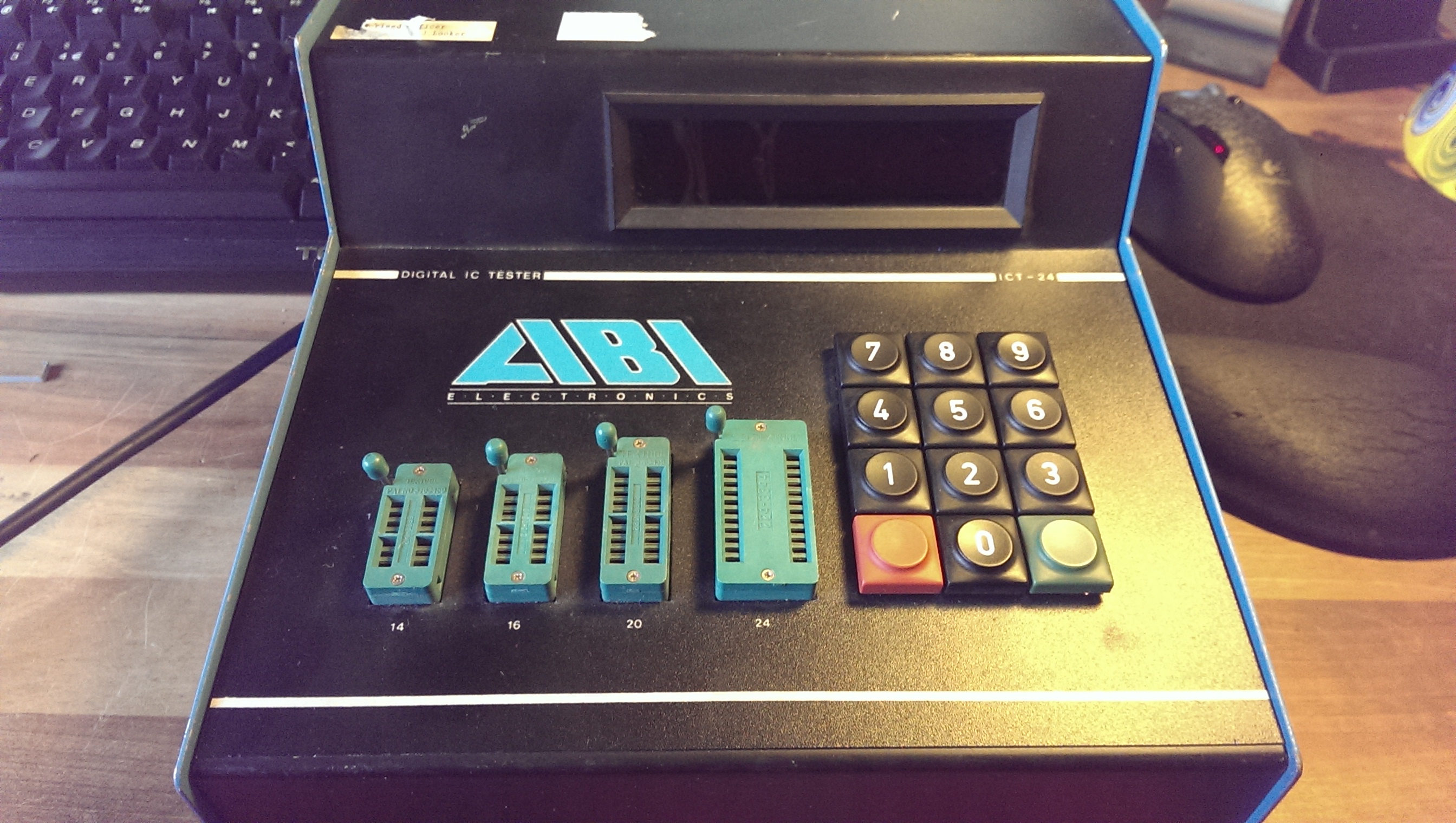
I recently found one of these devices and being a lover of test equipment I decided to see what it was all about.
IMAG1835

There is very little information about these online. The only official mention I can find about them is on ABI’s website and it just makes a passing reference to it stating it was the first IC tester device they made.
All other information comes from Equites who has had one of these for a number of years now. He has dumped the ROM’s from his unit and they are available in the downloads section.

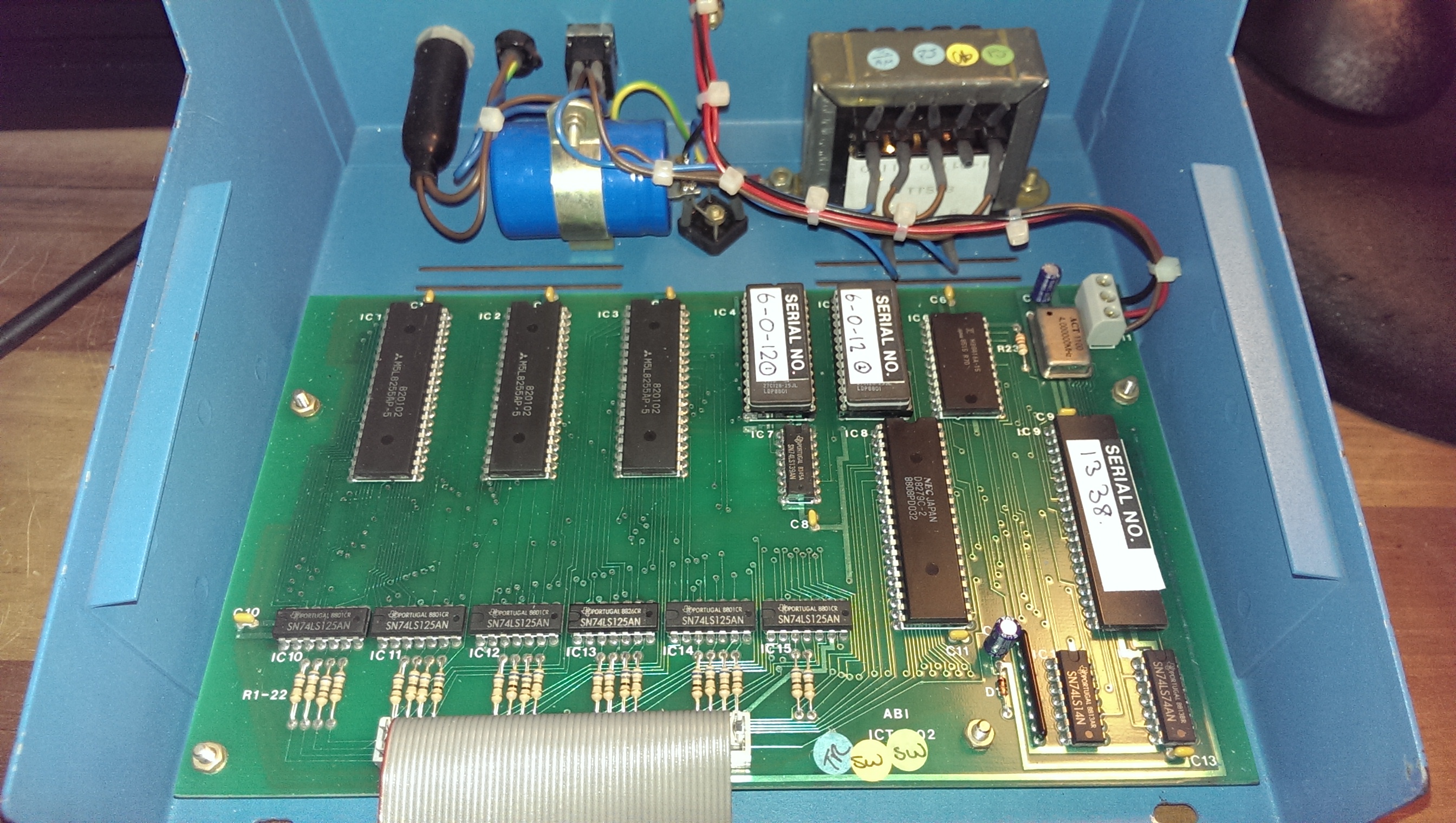
So, I got my unit and powered it up to make sure it worked. Once I had confirmed that I opened it up.
IMAG1837

I could see straight away that I have a different firmware version, mine being 6-0-12 and the version Equites has was 5-9-12. I’m still not sure what the difference between the two is.
So I dumped these EPROM’s (available in the downloads section too) and created a schematic for the unit.
The device is a Z80 based system with a couple of EPROM’s, a RAM chip, a keyboard/display interface chip and three PPI chips to control IO reading/writing.

Once I had drawn it out I derived the following memory map
$0000-$3fff – ROM1
$4000-$7fff – ROM2
$8000-$87ff – RAM

8255 (IC1)
$c000 – PORTA
$c001 – PORTB
$c002 – PORTC
$c003 – Control

8255 (IC2)
$c004 – PORTA
$c005 – PORTB
$c006 – PORTC
$c007 – Control

8255 (IC3)
$c008 – PORTA
$c009 – PORTB
$c00a – PORTC
$c00b – Control

8279 (IC8)
$c00c – Data
$c00d – Control

IC1 – Controls the /OE lines to all the IO buffers
IC2 – Controls the inputs the the IO buffers
IC3 – Controls the reading from the ZIF sockets

The ROM’s, RAM, 8279 and 8522 chips enable lines are controlled via 74LS139 decoder chip.

The version number of the firmware can be displayed by keying in “005” on the keypad.
On my version it displays “6-0-12” which matches the labels on the EPROM’s.
Interestingly the “6-0” is stored as data in the ROM while the “-12” is hardcoded as instructions starting at $11cd.
The first 2 digits, in my case “6-0” represent the software version.
The remaining digits are the options installed. Mine as options 1 and 2 installed.
Option 1 is for memory devices
Option 2 is for interface devices

The unit does a power on self test which displays a fault code between 0 and 6. These may be explained in the manual which I don’t currently have so I took apart the disassembled code to see what they meant.

Fault 0:
One of the IO’s is tied to GND.
The software tristates all the IO pins via IC1 (8522) and reads them back via IC3 (8522). They are held at logic HIGH via a pull up resistor network. If any pins are low this will result in FAULT 0.

Fault 1:
One of the IO’s on PORTA is tied to VCC.
The software sets all of the IO pins on PORTA to logic LOW and reads the states back. If any pins are found to be logic HIGH on PORTA then this will result in FAULT 1.

Fault 2:
One of the IO’s on PORTB is tied to VCC.
The software sets all of the IO pins on PORTB to logic LOW and reads the states back. If any pins are found to be logic HIGH on PORTB then this will result in FAULT 2.

Fault 3:
One of the IO’s on PORTC is tied to VCC.
The software sets all of the IO pins on PORTC to logic LOW and reads the states back. If any pins are found to be logic HIGH on PORTC then this will result in FAULT 3.
NOTE: The 2 uppermost bits on PORTC are not used for reading back IO lines.

Fault 4:
Fault with the program RAM.

Fault 5:
Fault with display RAM.
RAM should be 0x0. If it is not then FAULT 5 with be displayed.

Fault 6:
Fault with display RAM.
RAM should be filled with alternating 0x55 0xAA. If these values are not correct then FAULT 6 is displayed.

Equites supplied me with some additional pictures and a manual for these units and apparently there is a rebranded RS version too.
That’s about it. I have commented a lot of the code and learnt a great deal about how it works.
Its a very robust unit and no doubt it will get some use despite having other methods available to test. Its much more appropriate to have in a garage workshop.

If anyone can offer any further information about this (or feels the need to emulate it) then please get in touch.
Thanks to Equites for his information and scans.

 Posted by at 1:14 pm

Super Space Invaders ’91 PAL dumps added

 PAL Updates  Comments Off on Super Space Invaders ’91 PAL dumps added
Jan 012016
 

I dumped the two PALs from a Taito Super Space Invaders ’91 PCB (single layer version).Both dumps are tested and working in a GAL16V8 targeting device.

 Posted by at 12:04 pm

Bosconian repair log #1

 PCB Repair Logs, Repair Logs  Comments Off on Bosconian repair log #1
Dec 282015
 

I got this original namco untested pcb as a part of a deal.

As always happens, untested =not working and infact upon booting up it was totally dead with only a fixed static screen.

I was not too worried because I had a Dig Dug by Sidam which I use for spare parts and there are also schematics available (by Midway).

So I began my troubleshooting.

I checked the clock on the 3x z80s and it was missing.

Traced back to a dead output of a 74128@6B. The input coming from custom 07xx was OK.

clock

I started to search for a replacement and I took my Dig Dug pcb but in place of the 74128 there was a socketed 7402.

Bad luck, someone put wrong TTL as a place holder….

I then discovered that this 74128 is not common at all and it is used only on early namco pcbs.

I decided to contact my friend Charles Mcdonald to have a suggestion how to make the pcb boot just at least to see if it hadn’t other faults.

He told me that this 74128 is a really weird choice because it is used to drive signals over long distances and a 7402 is the equivalent to drive lower mA,  but I had to disconnect the R5 100ohm resistance.

In the end the guys at SIDAM made this “modification” on purpose to the original Namco design!

So I fixed the clock problem installing a 7402 and lifting provvisorily the resistance.

Foto 26-12-15 12 20 49

After booting up, unfortunately the game had another issue:

Foto 21-12-15 23 21 28

Foto 21-12-15 23 21 32

Foto 21-12-15 23 21 52


After some studying of the pcb schematics and some short circuiting I discovered that beneath these stripes there was the black background with the

stars correctly generated by the custom.

Worth of note is the score part of the display that was good.

On the video pcb there were 4x 4kx1bit rams 2147 which I didn’t have as spares (Dig Dug uses another video board) , two of them were running very hot .

Tested with the logic probe they were pulsing correctly.

At this time it was clear that the problem came from around there because shorting some pins changed the coloured stripes.

Disabling the CS line of the rams, restored good backdrop, stars and enemies but your ship and missiles disappeared.

So it was clear that these stripes where the “scattered” colours which should have been combined to make the ship correctly coloured.

I decided to test with the logic comparator the 74174@7D which is mixing the bits from the rams : it reported some bad pins.


mixing

When I changed it I got no better results, but I got another positive feedback that the problems came from the circuit near the rams.

If I left out completely the chip from the socket I got good backdround and no ship.

The enemies and bases are part of the background circuit.

All the TTL which were used to address the rams were good so it was clear that some or all the 4x 2147 rams were bad.

At this time I decided to give up and to order some new rams in the hope that the problem was really there.

Just before placing the order I decided to take another look at the 2148 ram @4J which on my pcb was not placed and I thought of a schematic mistake.

rams


Now everything was clear : Namco prepared already the pcb to accept one 2148 ram which is 1k x 4bit instead of 4x 2147 rams, 4 k x 1bit !

The highest addr lines are not used so it can really be used as a replacement!

I had a lot of 2148 rams so I immediately desoldered all 4x 2147 rams and placed @4J the 2148 ram

Foto 26-12-15 11 50 24


Foto 26-12-15 12 16 02


Finger crossed and when the game booted up I was finally welcomed with correct colours!

Foto 26-12-15 12 15 34

Haunted Castle repair log #2

 PCB Repair Logs, Repair Logs  Comments Off on Haunted Castle repair log #2
Dec 282015
 

Got this pcb from a friend of mine for a repair

haunted

The pcb had already all the sram chips repaired and some flying wires underneath because of broken traces.

Upon boot up, it constantly reset with this message:

haunted1

First thing was to test the socketed sram chip 6264 near the 2 big customs but as expected they were good.

Tried to flex the pcb and it booted with wrong palette sometimes

haunted2

Surprisingly once it booted it could be played with wrong palette all the time until the next boot.

So the code did only a check at the beginning.

After pressing and flexing everywere I found out that the game booted only when I pressed the Hybrid module 007327

I discovered looking underneath that the module has some small srams and looking at the schematics this is confirmed.

haunted_007327

I turned out that one pin had a subtle loose contact. I reflown brutally everything to make it more resistant against shocks.

haunted3

Booted the game and I was welcomed to a perfectly working game

haunted4


haunted5