What this article is about: This isn’t a conversion “how-to”, there is too much missing information for this to be used as such. It won’t teach you how to make a conversion since this is Strider specific.
This is more aimed at providing some technical info on cps1 and documents the process & tools used to fix a poorly converted game.
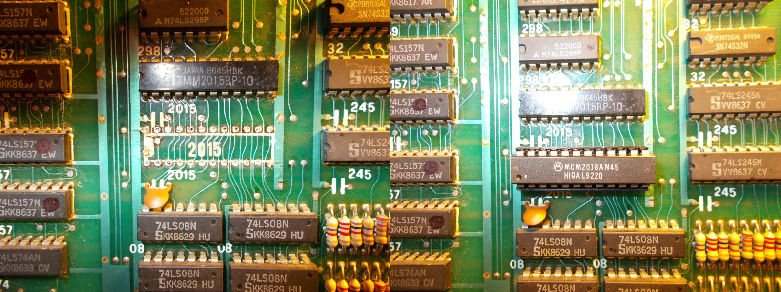
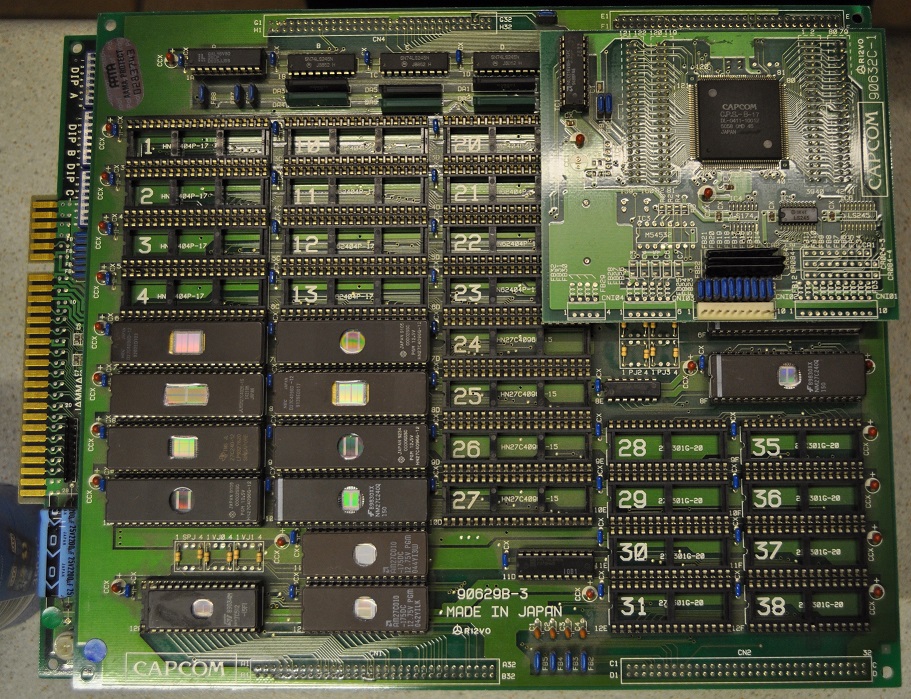
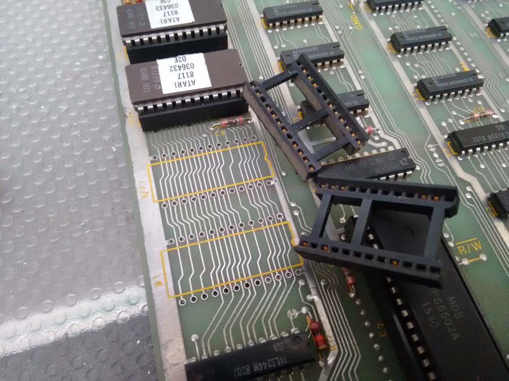
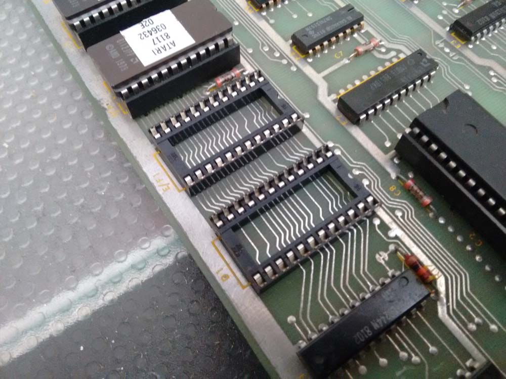
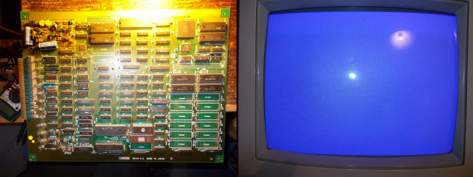
A rather interesting post came up from system11 on The Dumping-Union. Binaries were included of the images dumped from the EPROMs on the boardset pictured below.
This came from someone non-technical and with good reputation who worked
at Capcom US arcade section (proveable), he bought it from Capcom directly
(claimed but I see no reason to disbelieve) and seemed shocked when I
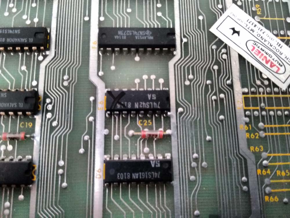
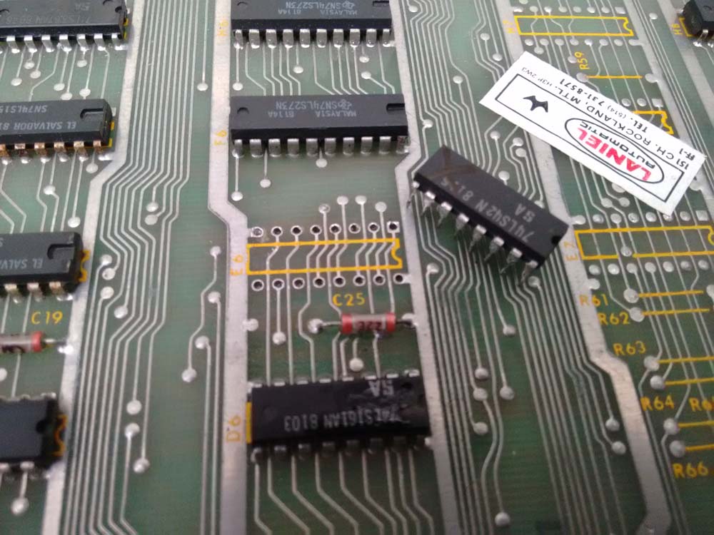
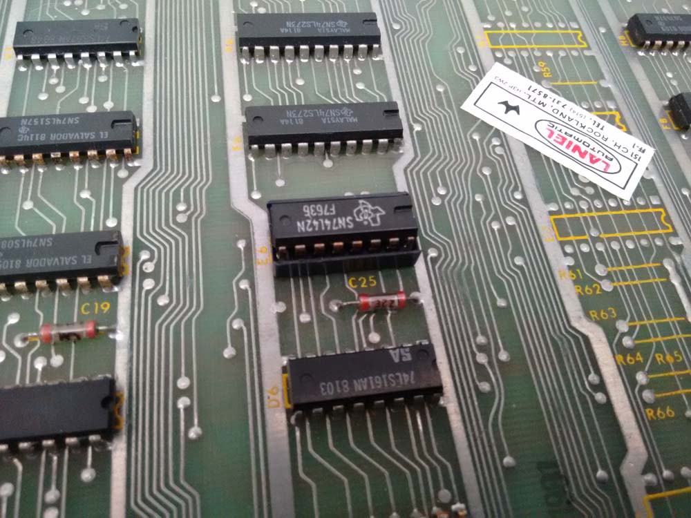
complained about it being converted. We’ve got a GAL on there which I
can’t read, a bunch of chip matches in wrong locations and an unknown code
ROM. No jumpers have been moved. Clearly converted from a SF2 variant.
No idea why this exists.
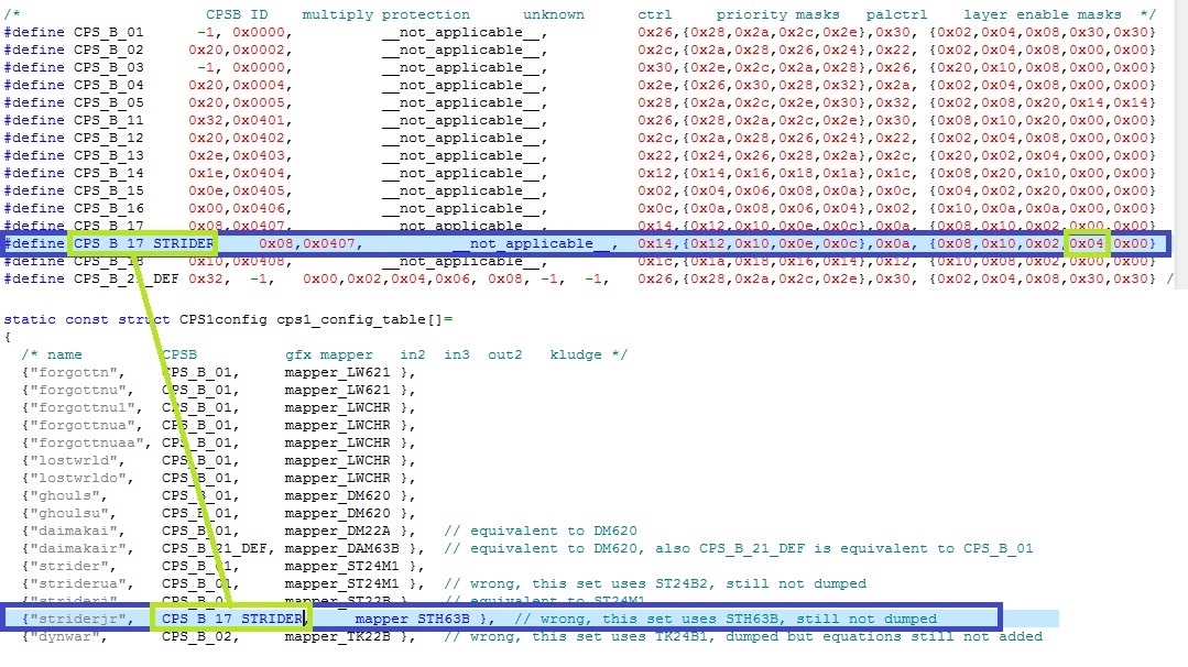
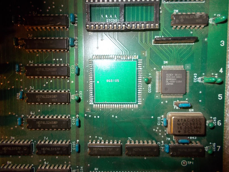
So what we have below is a 90629B-3 B board populated to run Strider on a 90632C-1 C board with the CPS-B-17 PPU. The only CPS1 game to use this specific PPU was Street Fighter II: The World Warrior however, being a popular game Capcom used many different variations of this PPU.

What makes this particular conversion interesting is that according to system11, the PCB was purchased from a Capcom source who purchased it in-house.
It was bought from xxxxxxxxxxx:
He bought it when the Capcom arcade unit in the same building was winding down as I understand it. He claimed not to know it was a conversion when I received it, and honestly given his background I do believe him. Probably a half finished tech project by one of the engineers.
Nobody can claim that this is an official “Strider” system, at best it could be described as an “in-house” conversion, poorly done but the engineers who worked on this obviously had better and more important things to do with their time.
There are several code related issues which prevents the game from running properly especially after you die at certain checkpoints and also some other issues which I discovered myself.
So now it turns out that the game doesn’t actually work properly if you die in stage 2, does anyone have any ideas what I can do with this boardset?
Looks like it was a World Warrior to begin with – CPS-B-17, so I’m leaning towards ‘throw it away and sell the A board’.
Having a shitty month so far.
I decide I want to help out and fix the game. This makes for an interesting project as I have done several conversions in the past for myself & friends but I no longer own a complete CPS1 system. Testing would be difficult however, thanks to MAME I can do most of it via the debugger. I would send the new versions to system11 and he would test the changes on his PCB and report back.
The first step was to reproduce the problem in MAME. I’m using a very old & hacked up version of MAME (v1.50) which is fine for what I’m doing.
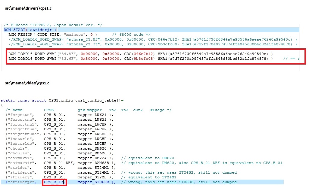
To do this I make some code changes to the cps1.c driver & cps1.c found in video. Changes are highlighted in red.
Note I am modifying the Japan resale version of the driver, the choice was arbitrary. You can see that I have run the USA version of the ROMs in this driver in the past 🙂

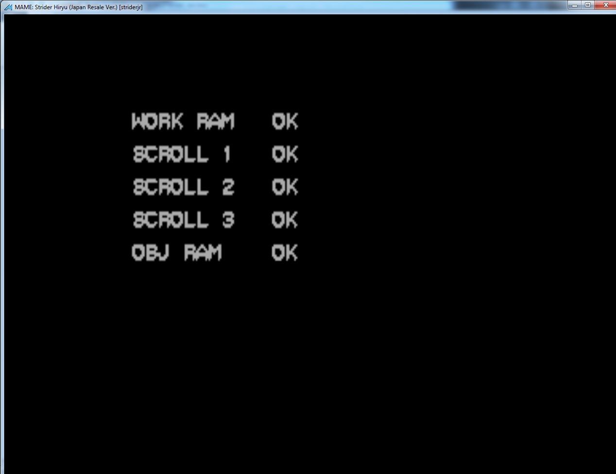
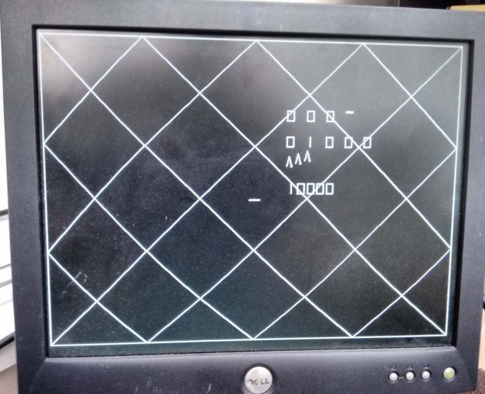
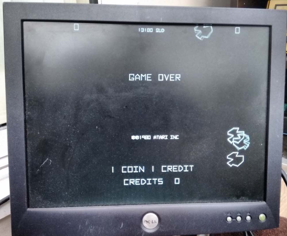
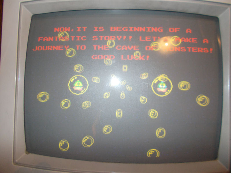
After re-compiling the code and running the game for the first time it was evident that their was a problem. Nothing showed up on the screen until the game entered the attract mode. Normally the post shows some text related to the power up tests. Since the screen is black until attract mode is entered there is nothing to show here.
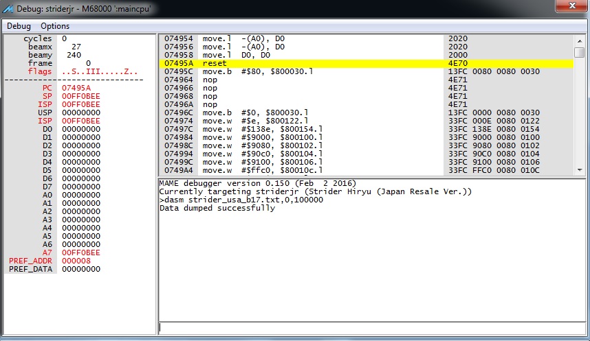
To see what is going on, I decide to disassemble the code via dasm in MAME which generates a 20Mb text file containing 68k code. A decent amount if you like reading through tonnes of code and have nothing else better to do.

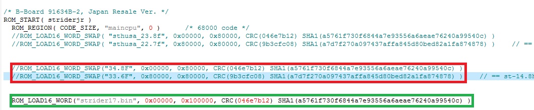
I also fire up the US Strider (USA, B-Board 89624B-2) and disassemble the code. The hack is based off this U.S version.
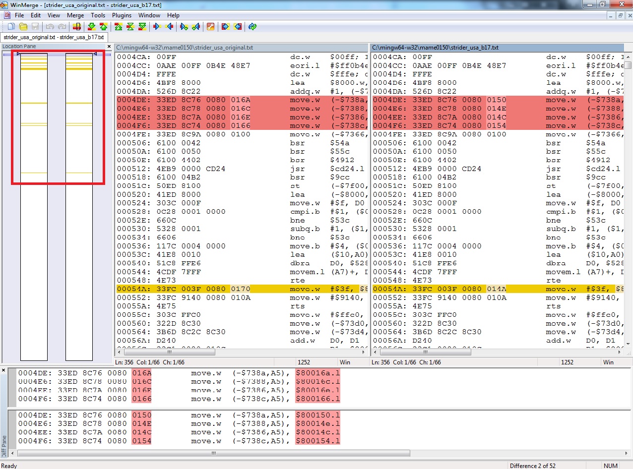
Combining both files side by side using WinMerge allows me to see the changes the hackers made to the original. There are a total of 52 differences. But even that wasn’t enough!

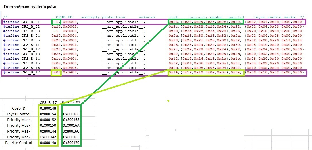
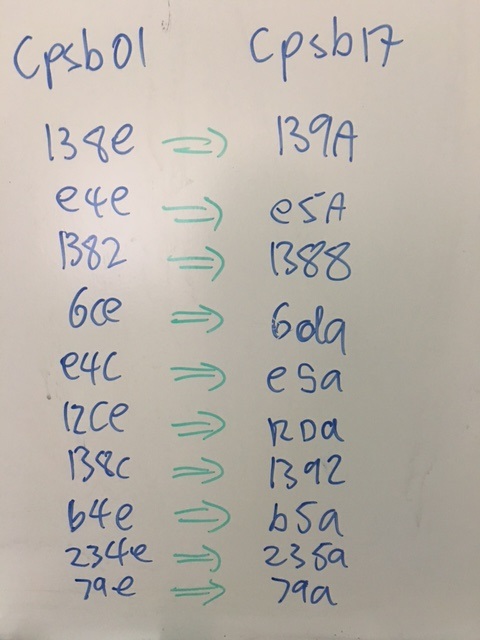
I need to create a small table which represents the difference between cps_b_17 & cps_b_01 registers. I also need to describe what each address register is for ( layer control, priority mask..etc ) These move between different PPUs. So why did Capcom do this ? Perhaps for security to stop operators from easily converting games who look to avoid purchasing conversion kits, sounds plausible.

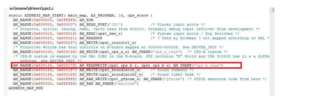
According to MAME, cpsb registers start at a base address of 0x800140 and end at 0x80017f, this is true for all cpsb PPU variants. But the actual addresses for each register changes between PPUs.

For cpsb17, to get the address for the layer control I simply add 0x14 to the base address of 0x800140 which gives me 0x800154. 0x14 is taken directly from the table above in src\video\cps1.c.To get the first priority mask I add 0x12 to the base address of 0x800140. I go on until I have completed the column on the left. Similarly, I do the same for the cpsb_01 column until the table is complete.
I can check the existing work and have something to guide me a long the way by using this table. I normally write all of these details on a white board.
Since the original game uses the CPS_B_01 PPU I have put them both side by side in the table above. So if I need to change the palette control I substitute 0x800170 (cpsb01 ) for 0x80014a (cpsb17).
I now have what I need to start working on the code but to make editing simple I dump the two rom regions and combine them into one file using the MAME debugger and edit the driver to accept the single binary file. I do this to make editing and testing the binary straight forward.
Changes in red are made by adding comments to the two lines and adding the line in green.
Later I’ll split the single binary into two files once I’m happy with the results so that they can be burned to the EPROMs.

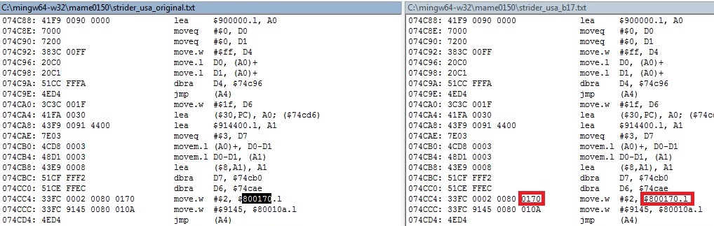
Using the cpsb table I begin by searching for $800170 in the right hand column of WinMerge, I repeat this process for each register in the table. This is just my process of checking existing work. Note that there are no differences at 0x074CC4, $800170 is the palette control register used by the cpsb01 PPU but the hackers missed that. It should be $80014a for the new PPU.

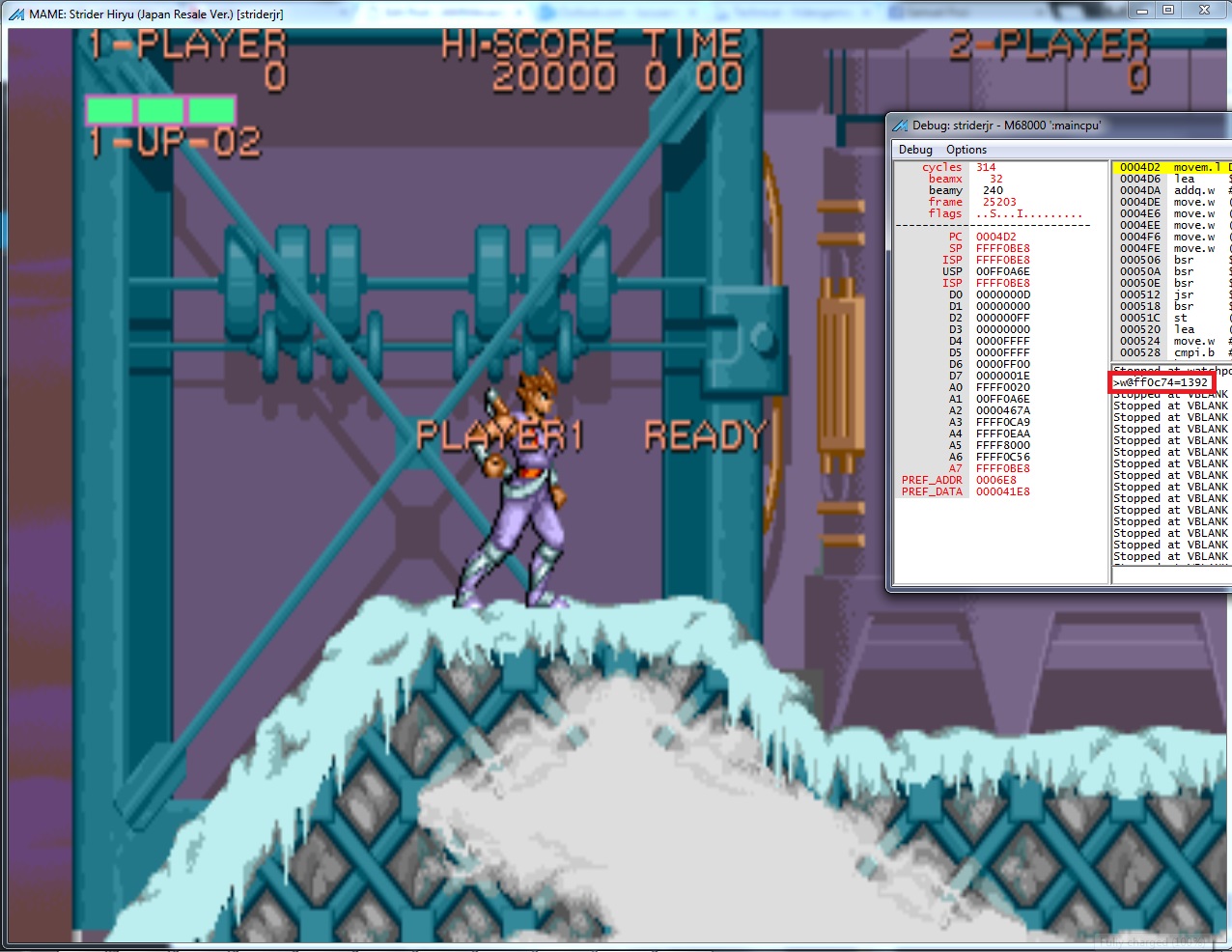
Cross referencing the table, I change 170 to 14a in strider17.bin using a hex editor. This fixed the post and the power up tests are now visible.

The game also had an issue with the sky not showing up at all, this was only reproduced in MAME & not on the real PCB. I try to find out why.

The bits for the layer enables are written to address 0xFF0C74 ( 0xFF8000 – 0x738C ) in DRAM before being written to the layer control ( 0x800154 ). The value written here is the old value for the cpsb01 chip. 0x138e is coming from a location in ROM pointed at by A1 ( 0xB616 ).

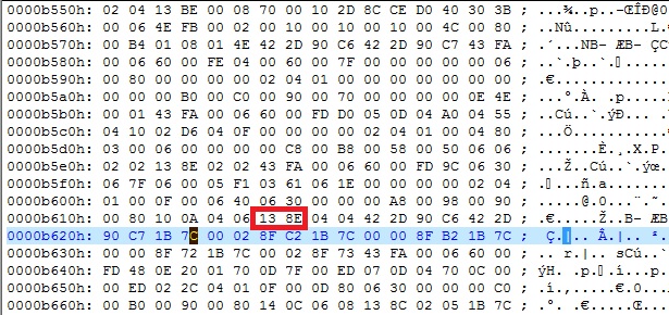
Here is the location in ROM that needs to be changed to 0x139a.

Changing it fixed my sky. Although the old value still worked on system11’s PCB, it still wasn’t correct. My changes never broke the sky on the PCB, so I’m happy with the change although it made no difference.
The sky is still missing in stage 1 & during the intro after you press start. But it’s not related to the problem found above.

To get the sky to show up correctly I had to tweak the enable masks in MAME. Street Fighter II: World Warrior is the only game that uses the CPS_B_17 PPU and not all the layer enables are used in the game, hence MAME only defines some of them which explains our missing sky in this instance. I could have left it alone as none of my changes require any alterations on the game EPROMs. It’s just nice to prove that missing stars has nothing to do with the PCB itself.
I create a new CPS_B_17 entry just for Strider as I don’t want to break Street Fighter. I then change the 4th layer enable mask from 0x00 to 0x04. I tried other values at first but 0x4 worked correctly. I also modify the config table to use the above new entry.

Recompiling MAME and running the game brings the stary sky back. So now I can move on to more important stuff.

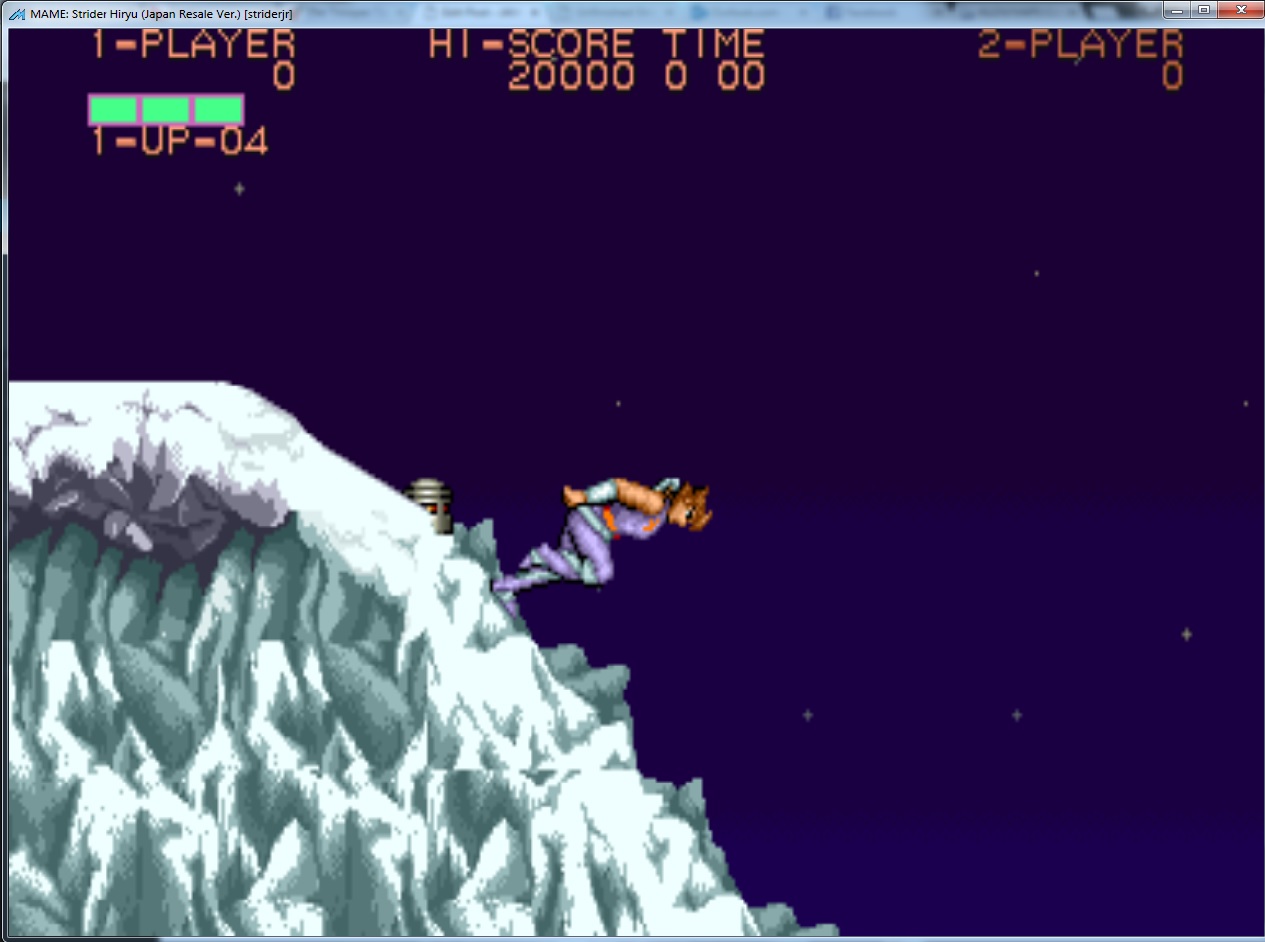
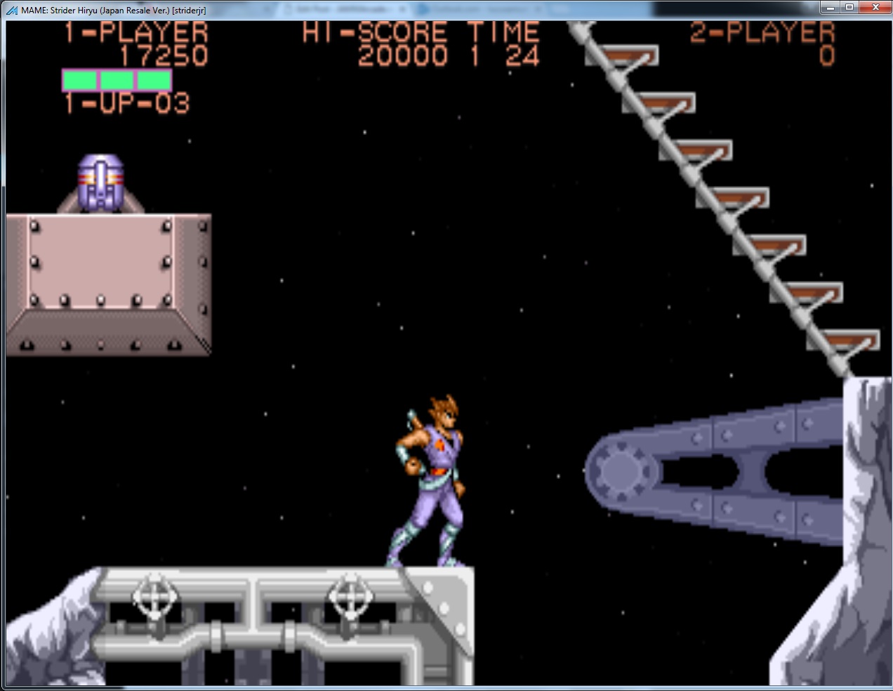
One of the complaints regarding bugs reported by system11 suggests that if you die at a certain checkpoint in stage 2 then the entire background disappears. I reproduce this issue by playing the game.

I know from looking at the screen that this is a layer enable problem. First I create a small table with the old enables for the cpsb01 board on the left and the cpsb17 masks on the right. The hackers have already done most of the work for me so I just go through all the differences for the layer enables which I found in WinMerge and make a note of them on my whiteboard to create the table below.

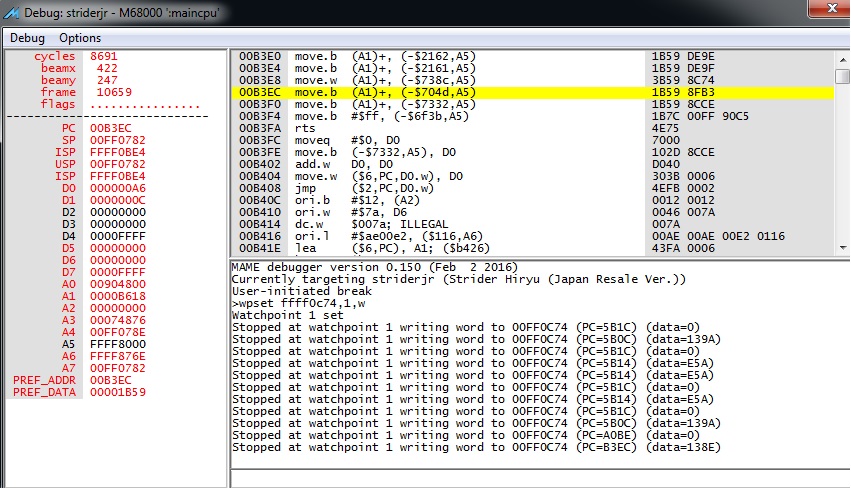
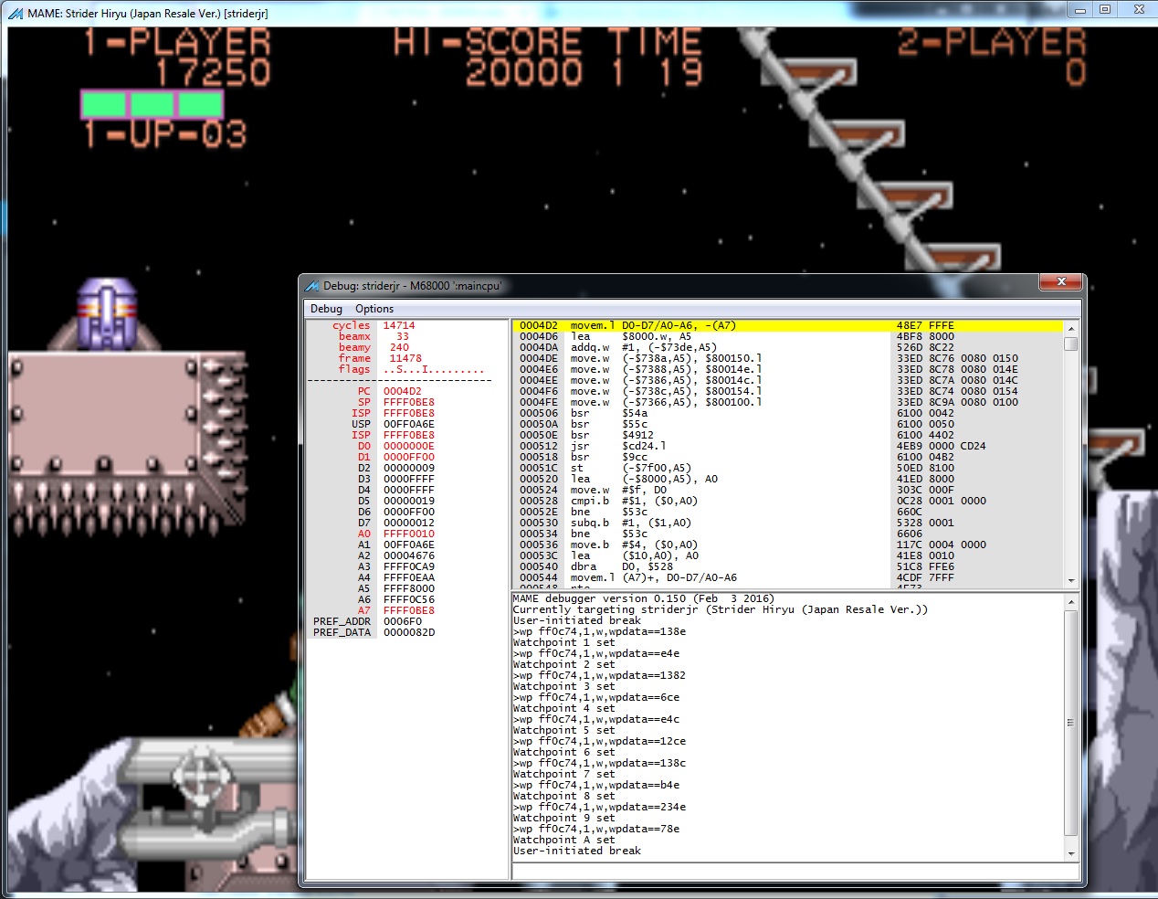
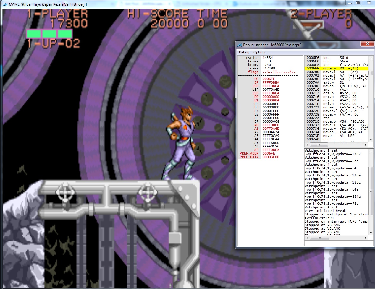
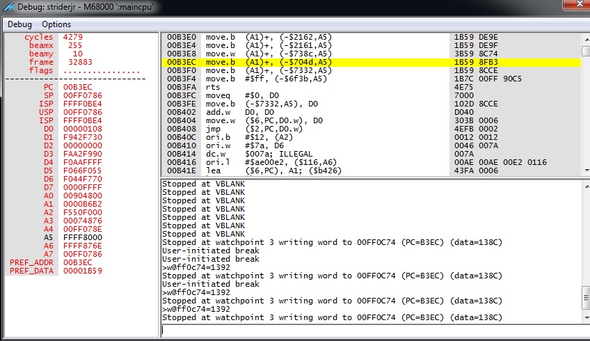
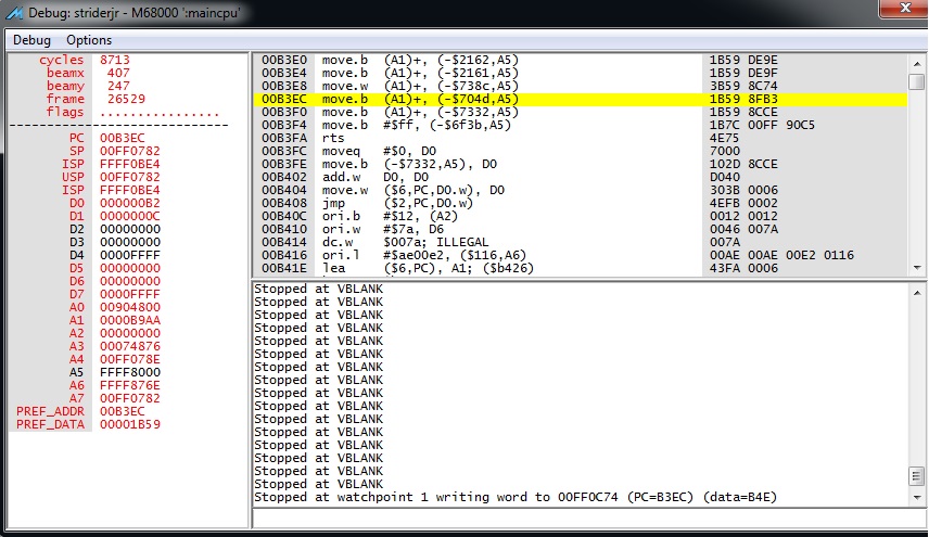
I then create a bunch of watch points which are invoked when specific layer enable bits are written to the DRAM address 0xFF0C74. The value stored here is used later on and written to the layer control register at 0x800154.

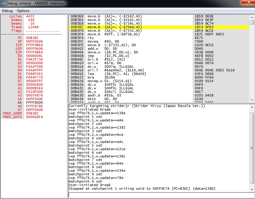
I play the game until I die and the debugger is invoked when the data written to 0xFF0C74 equals 0x138e. This needs to change to 0x139a to bring back the correct background.
The value 0x138e is read from A1 ( 0xb5e4 ) and that is the offset where I need to make the permanent change to the file.

But first, I want to see if overwriting 0xFF0C74 with 0x139a via MAME will bring back the correct background temporarily ( until I die at the same checkpoint of course ).
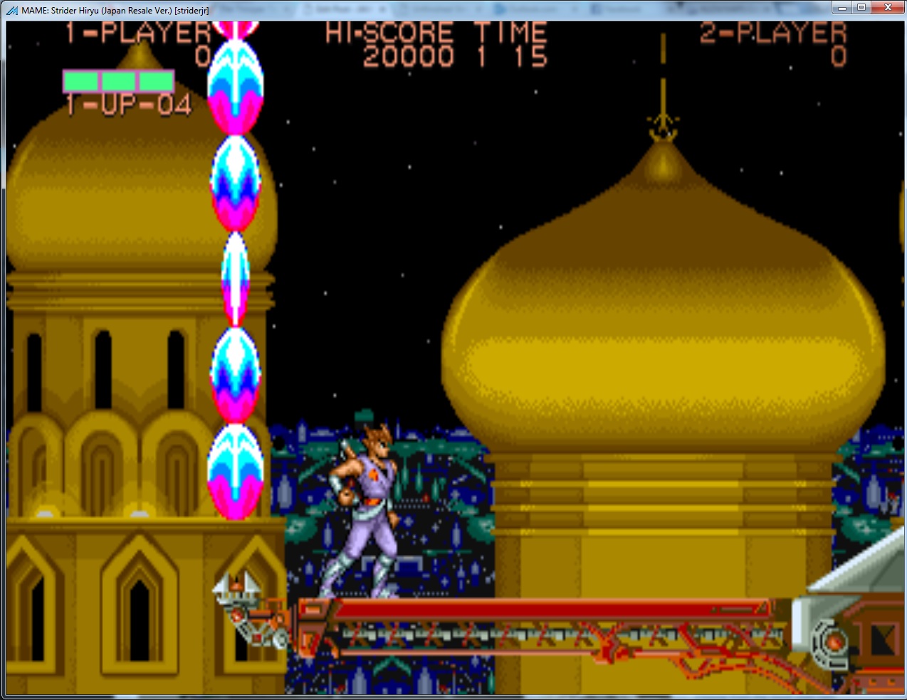
The changes worked as you can see below. So I’m definitely on the right track here.

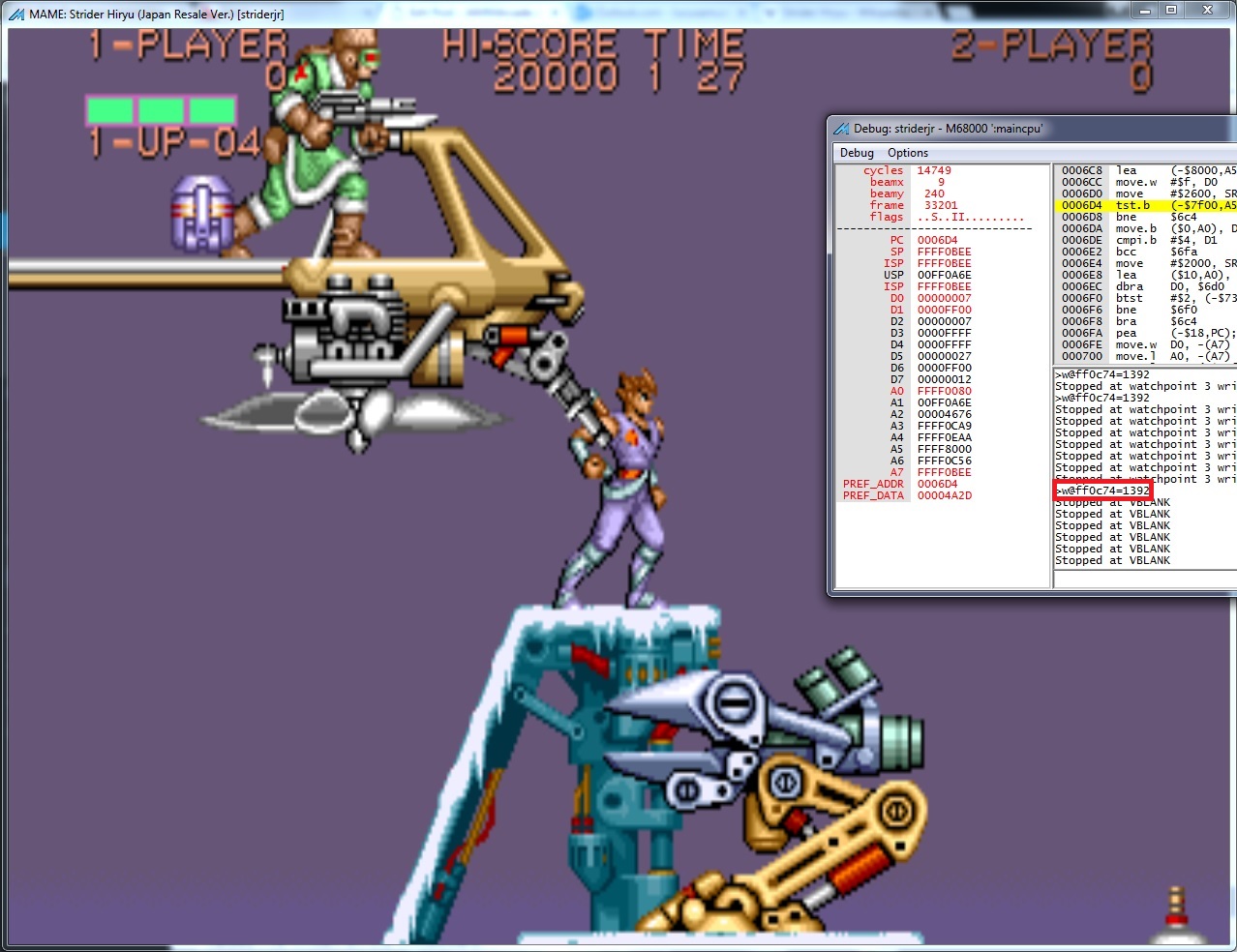
Here is another issue in Stage 2, the background completely disappears after dying ( next screenshot ). The debugger is invoked when it writes 0x138c to our DRAM address. This value comes from A1 which is hard coded at offset 0xB66C in the rom, i’ll change that value to 0x1392 later.

And here is the result if I resume program execution.
And the temporary fix by writing 0x1392 to DRAM: 0xFF0C74 which is later written to the layer control.

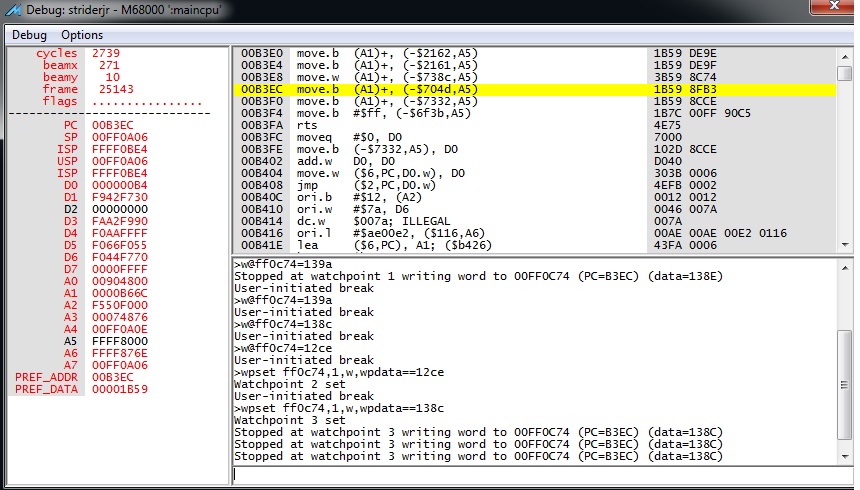
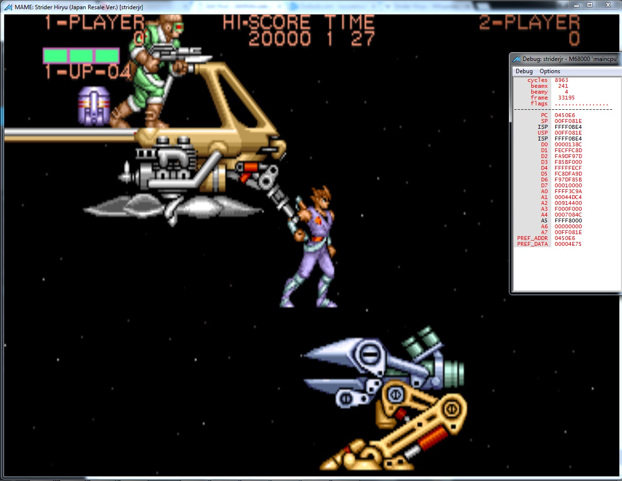
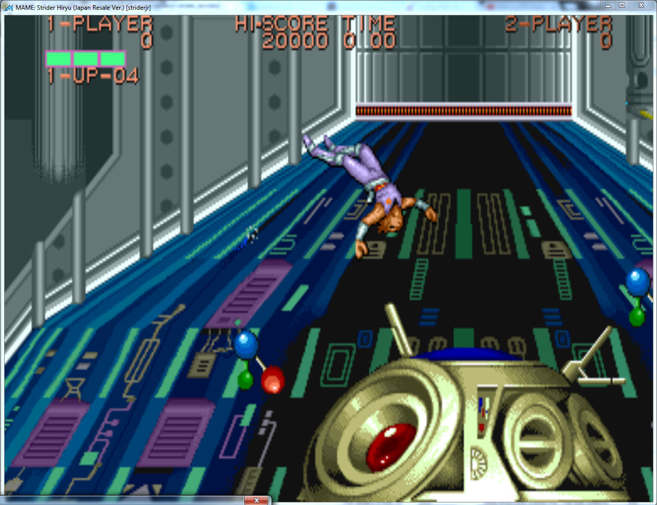
Continuing on in stage 2 brings me close to the end of the level where I head up towards the large airship. Dying triggers the debugger on watch-point 3 as the layer enable value of 0x138C is written. This value will later be changed to 0x1392 at offset 0xB6B2 in the rom.

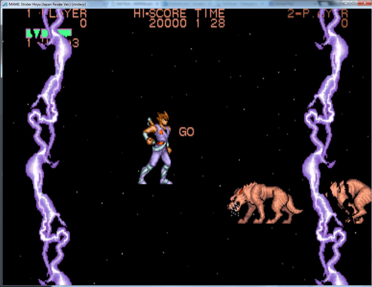
If I resume execution you can clearly see that the background is missing as Hiryu appears to be magically hovering in the sky.
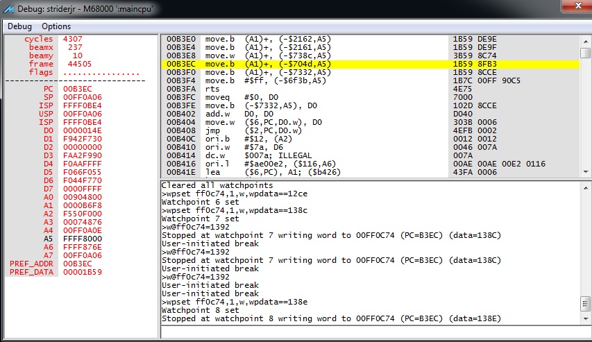
Fixed temporarily by writing 0x1392 to DRAM: 0xFF0C74.

Finally this brings us to the large airship at the end of level. Dying triggers the debugger as the layer enable value of 0x138e is written. This value will later be changed to 0x139a at offset 0xB6F8.

Resuming execution shows a stary sky instead of the correct background.

Fixed temporarily by writing 0x139a to DRAM: 0xFF0C74.

This concludes the fix as far as stage 2 goes, I couldn’t see anymore problems in this stage.
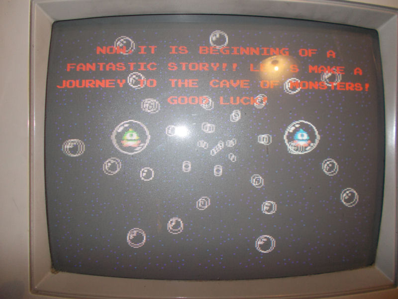
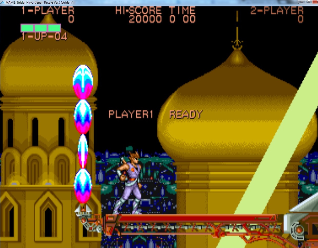
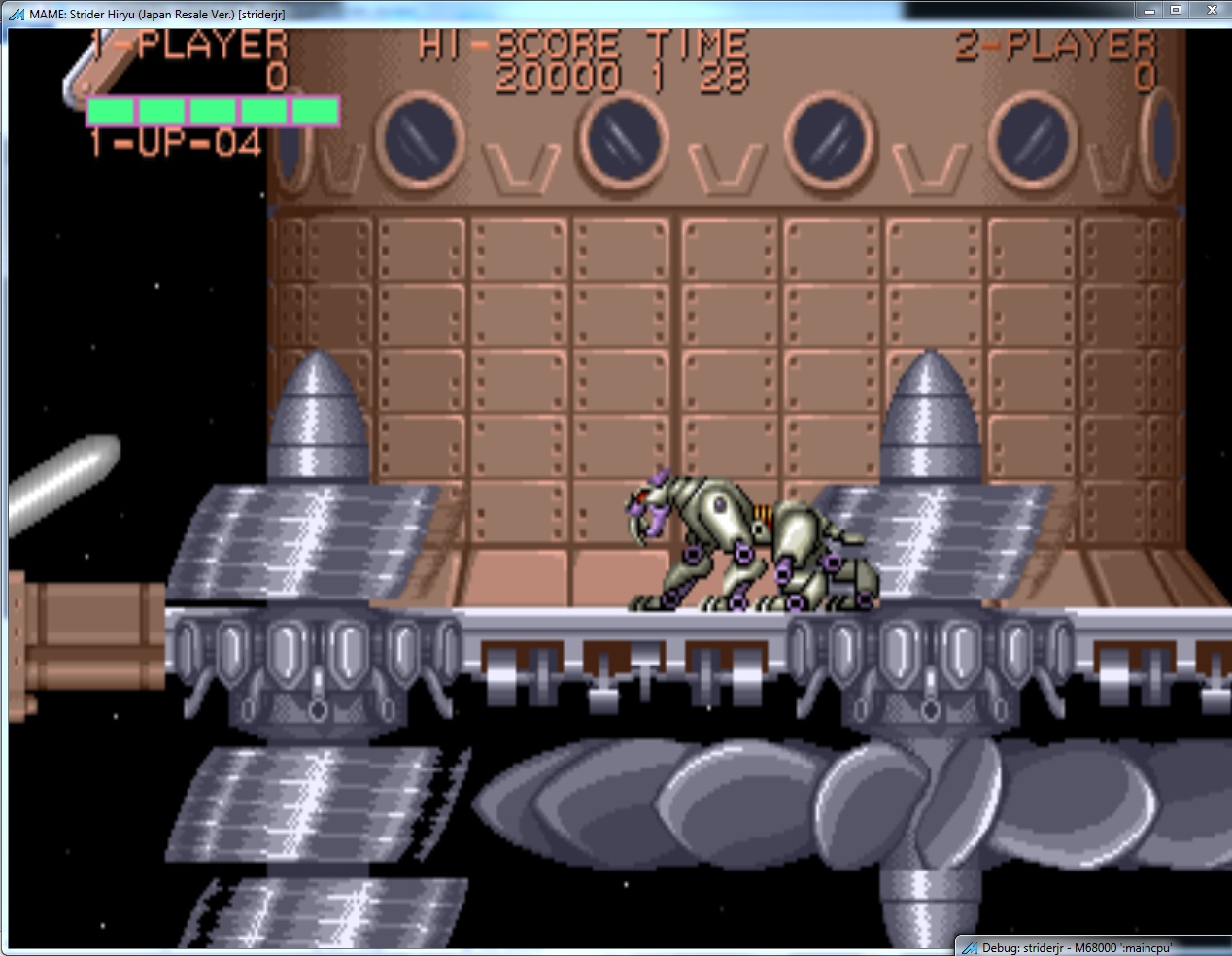
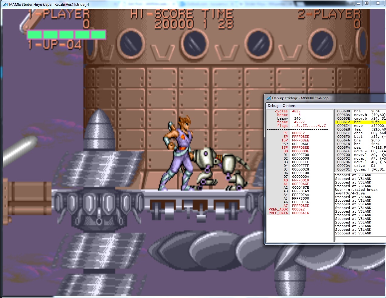
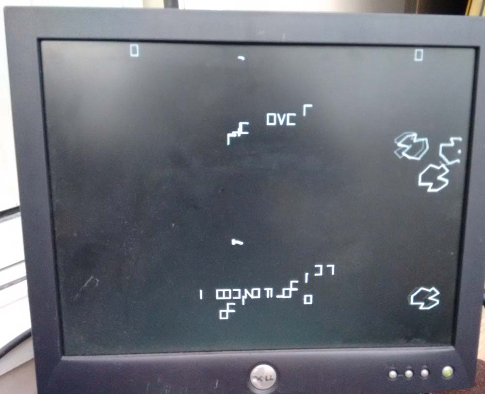
I still want to fix the issues in attract mode. So let us take a look at the two issues I found. First issue was the missing dinosaur, it only showed up briefly before it explodes. The second issue was the missing satellite.
With my watchpoints set the debugger pops up when the layer enable bits equals 0x12ce. This needs to change to 0x12da, this is done at file offset 0xB81A which is held by A1 in the debug window.

I’m quite confident at this stage that my temporary changes will work so I don’t bother with those, I edit the binary, restart the game and our dinosaur appears behind Hiryu in the attract mode.
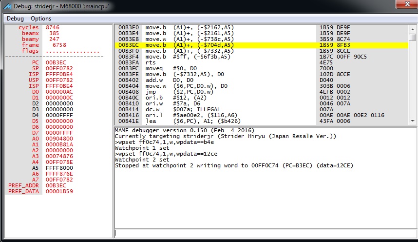
The other issue is the missing satellite. The fix needs the value 0xb5a instead of 0xb4e at offset 0xb9aa.

Editing the binary at the said location fixes the issue.
I still need to play through stages 3,4 & 5 to make sure there are no more surprises. Having my watch-points set and dying as often as I can will ensure that I cover all the bases ( hopefully ). There’s no difference to the process as documented above so I’ll just leave it at that.
I could have used a more shotgun approach and used a search and replace tool but then I run the risk of changing something I shouldn’t and breaking the game.
Once I’m happy with the changes the binary is split into two 512kb, word swapped and sent to system11 for testing on his PCB.

 ha
ha