Hello everyone, this time I have a Konami Asterix board that I got from the Arcade Museum forums.
I bought it as non-working “error with 2 chips” at an affordable price.
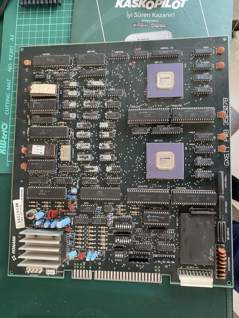
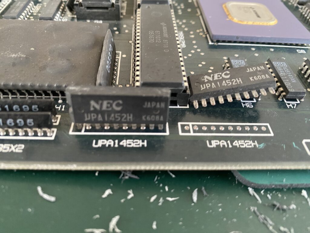
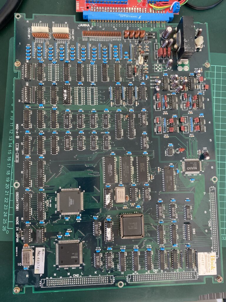
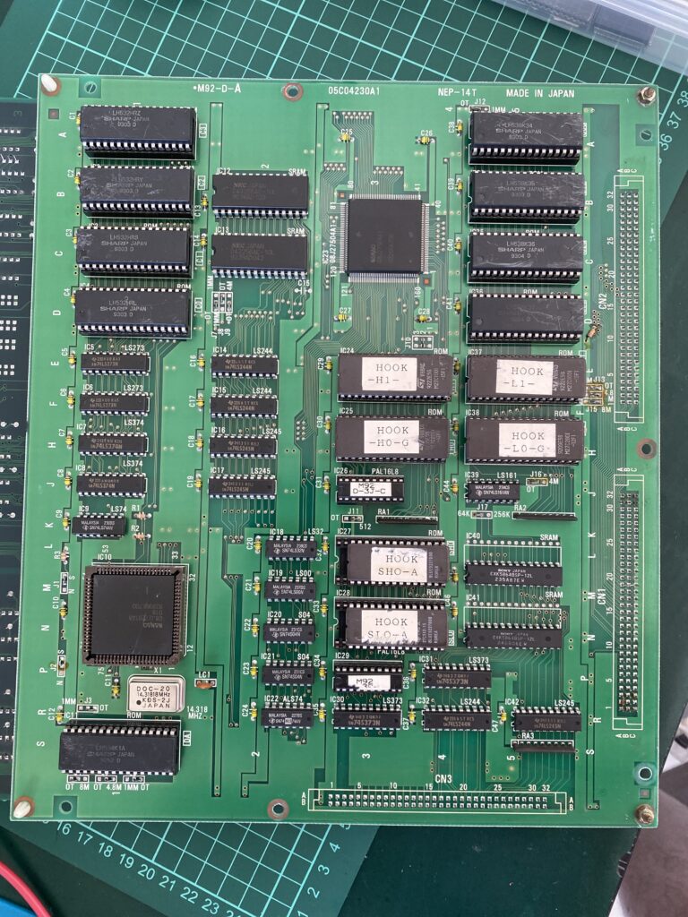
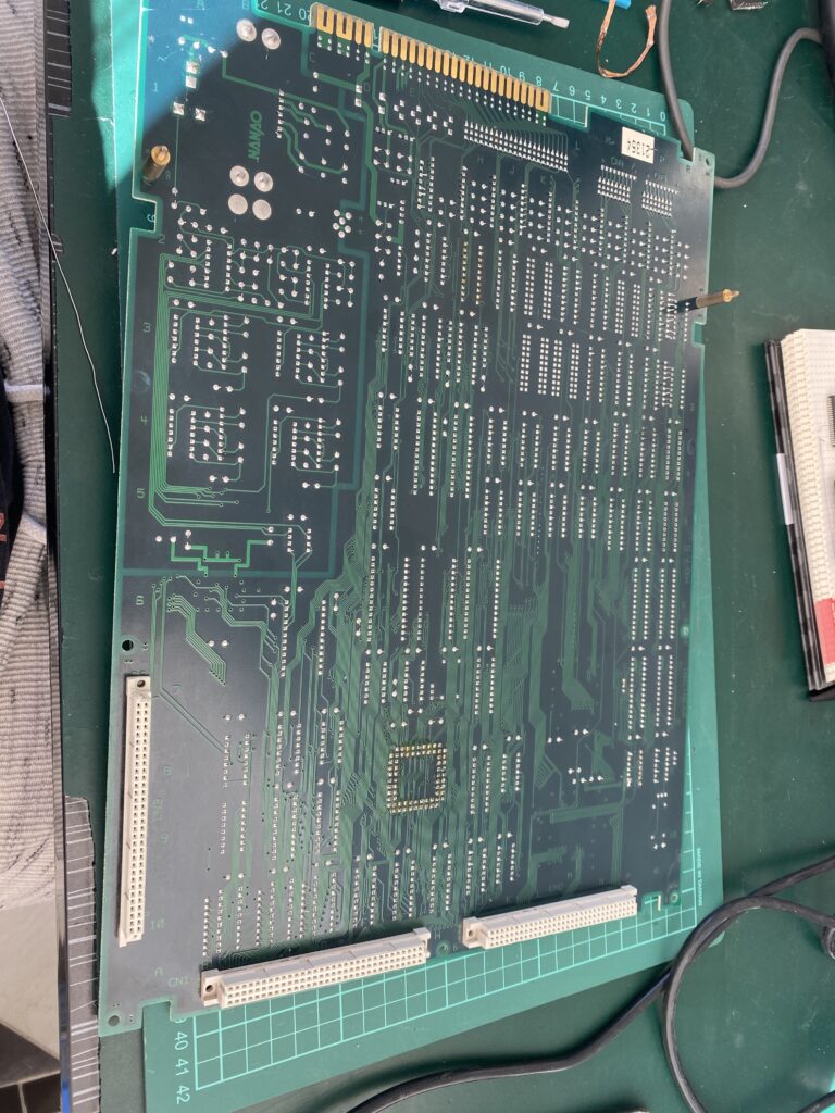
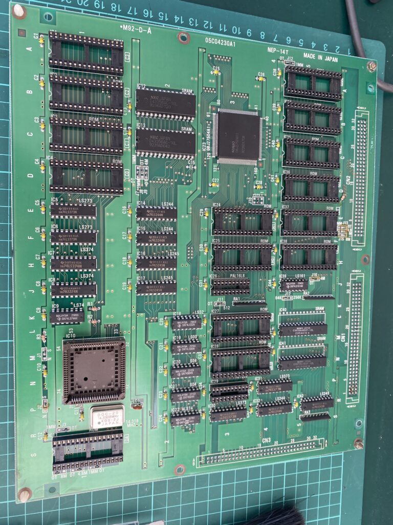
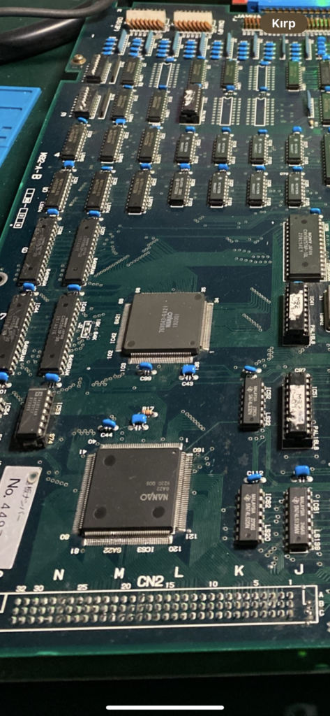
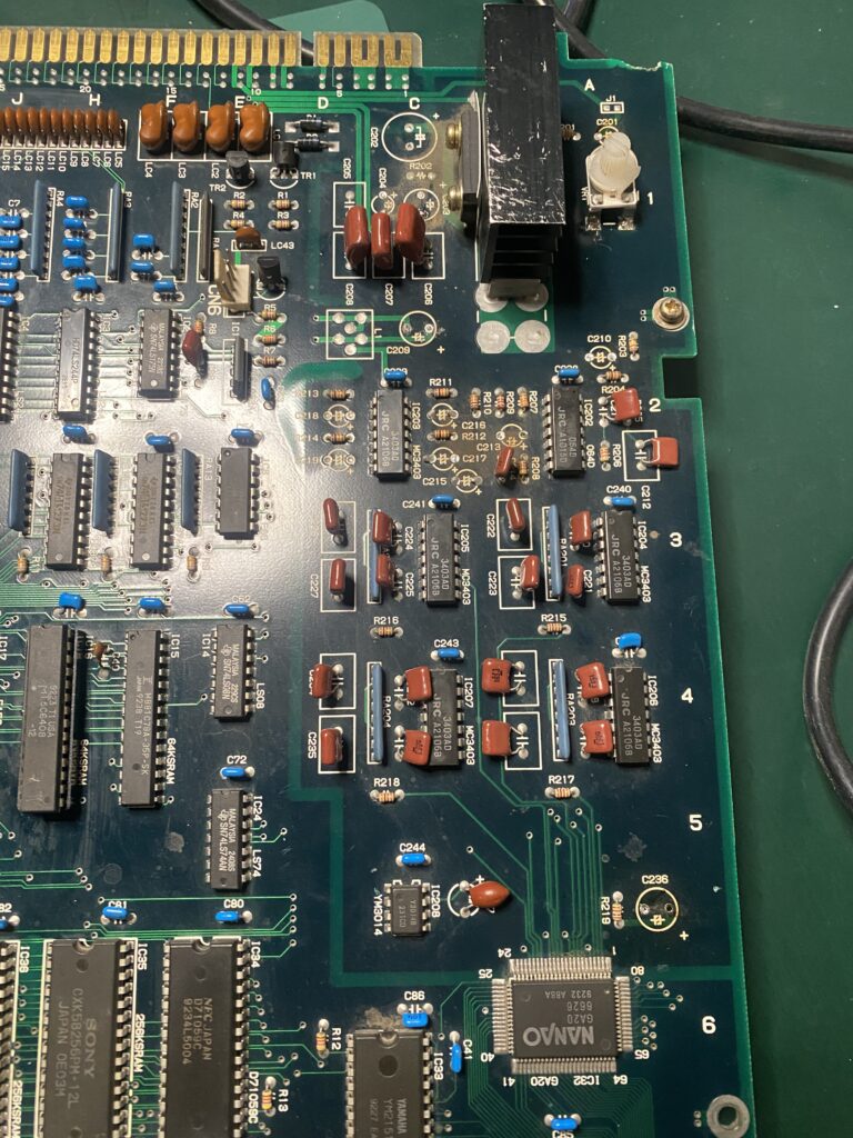
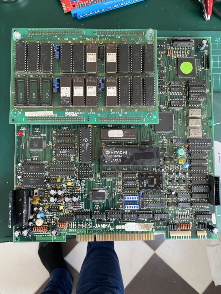
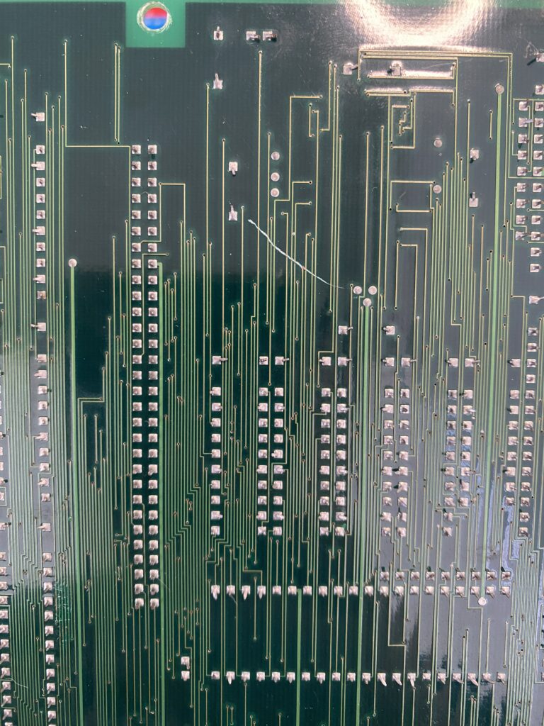
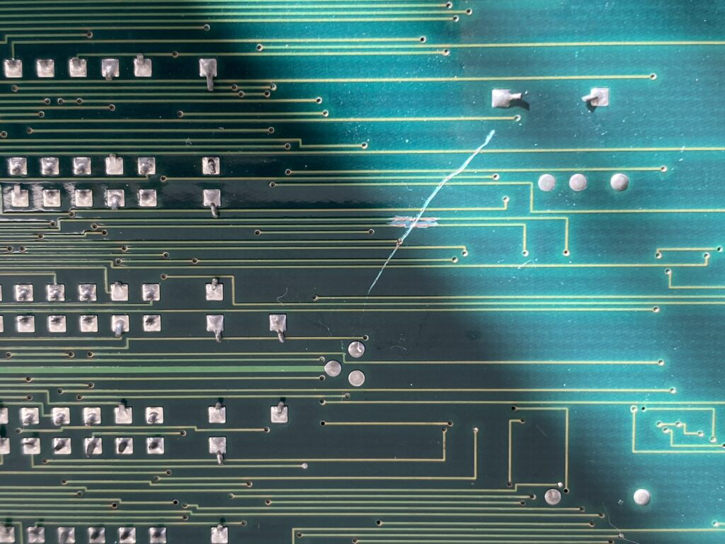
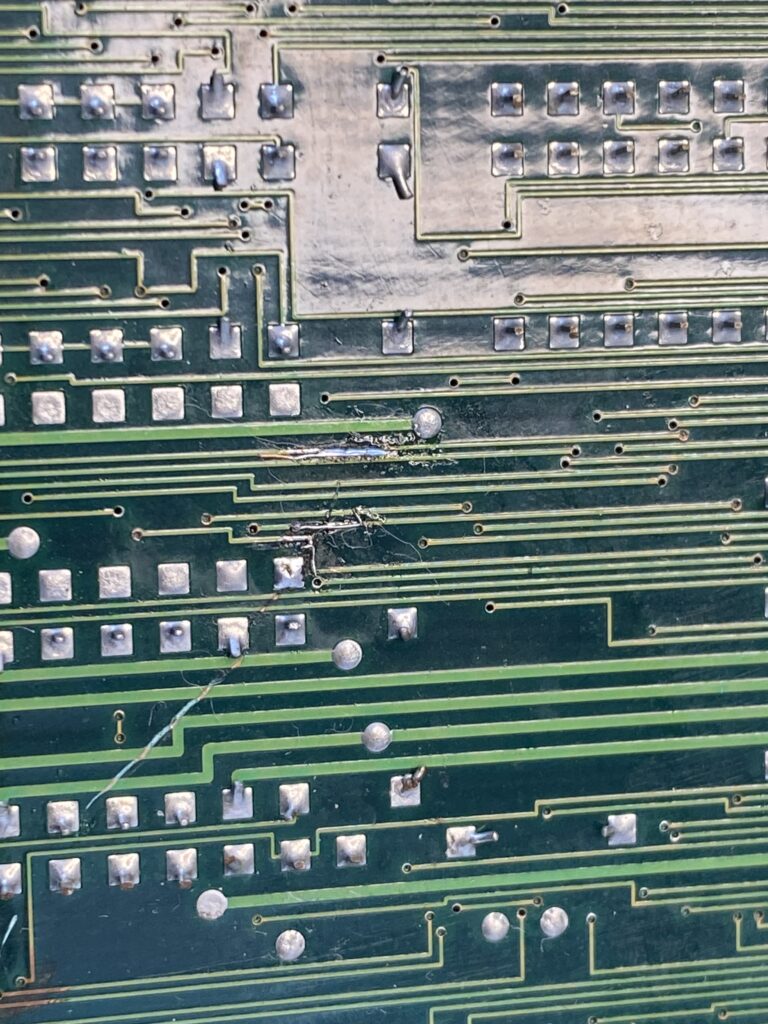
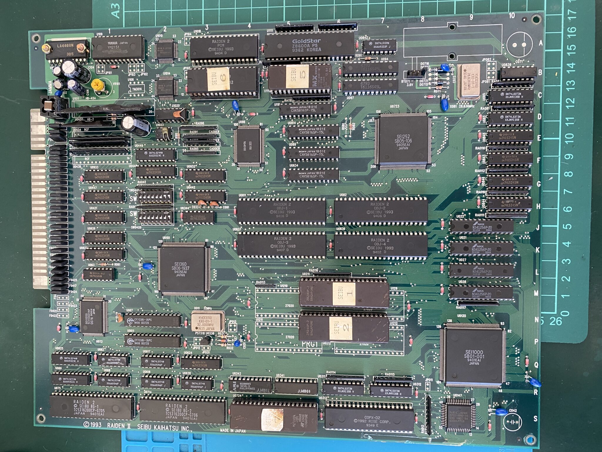
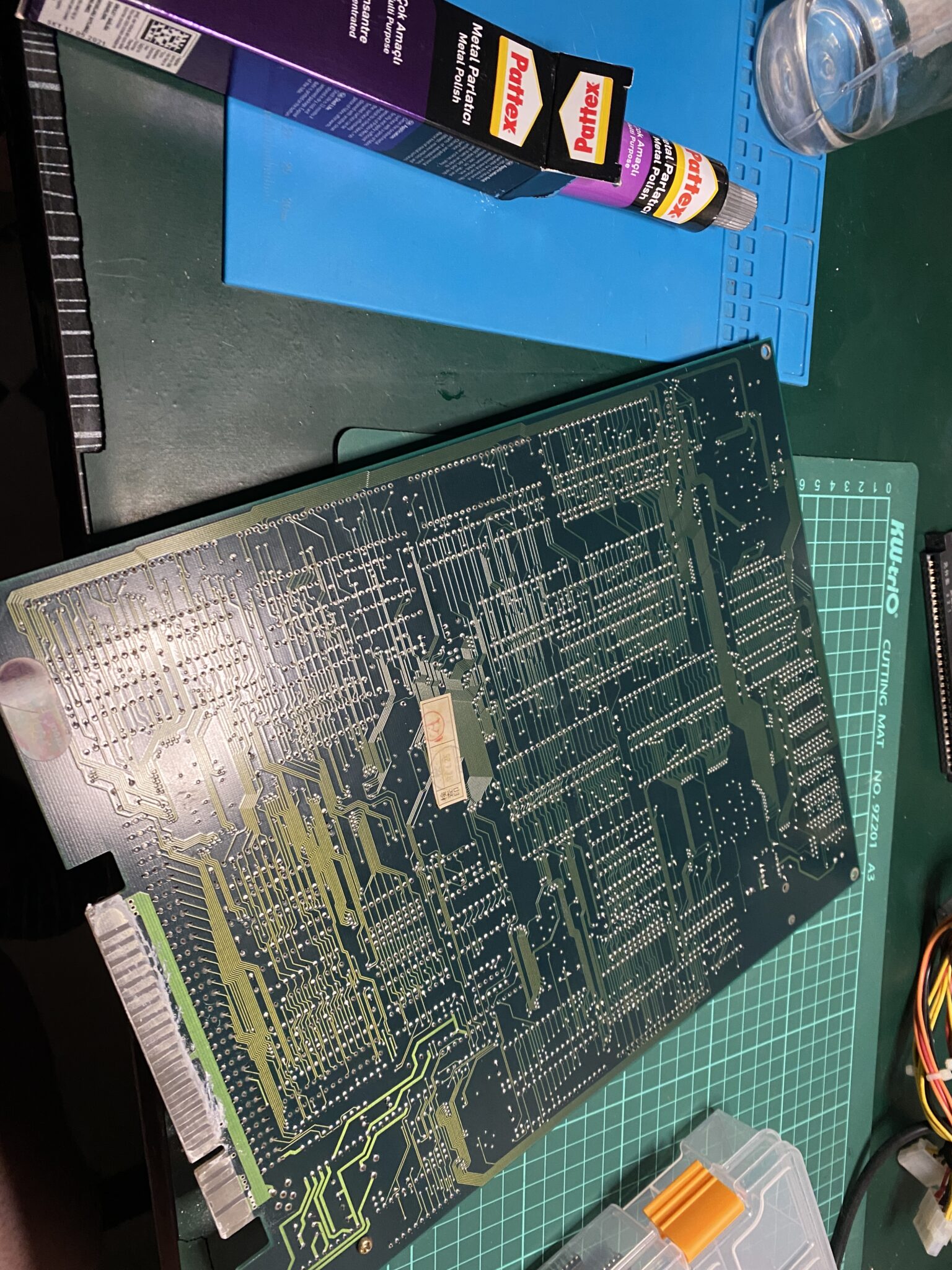
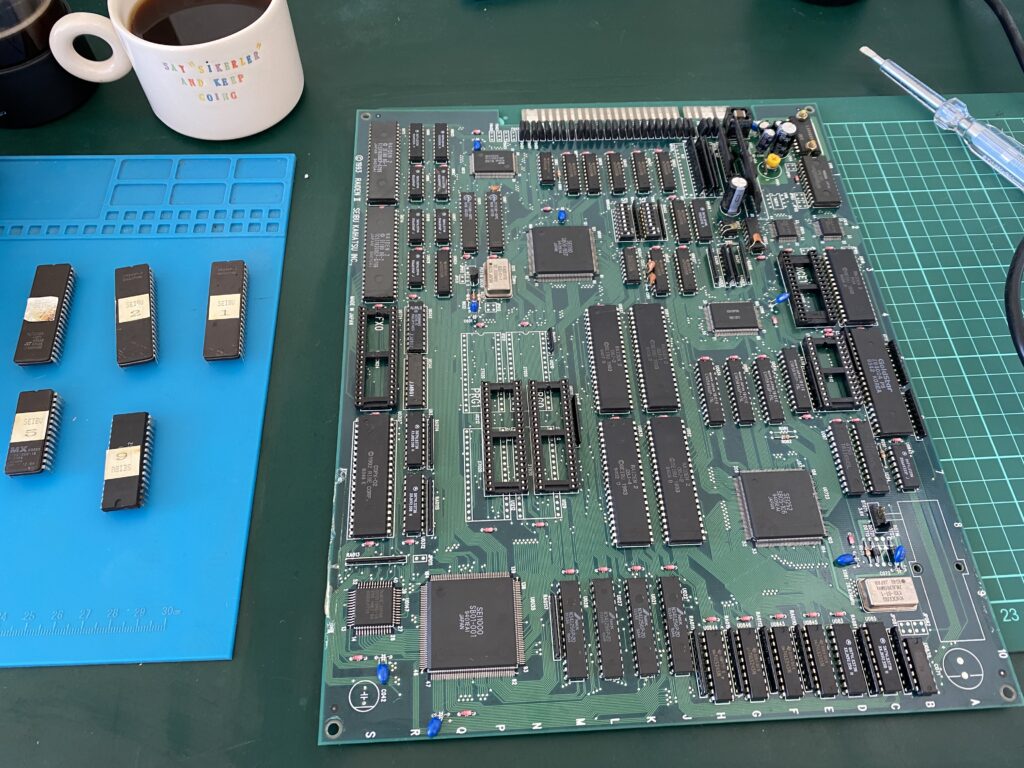
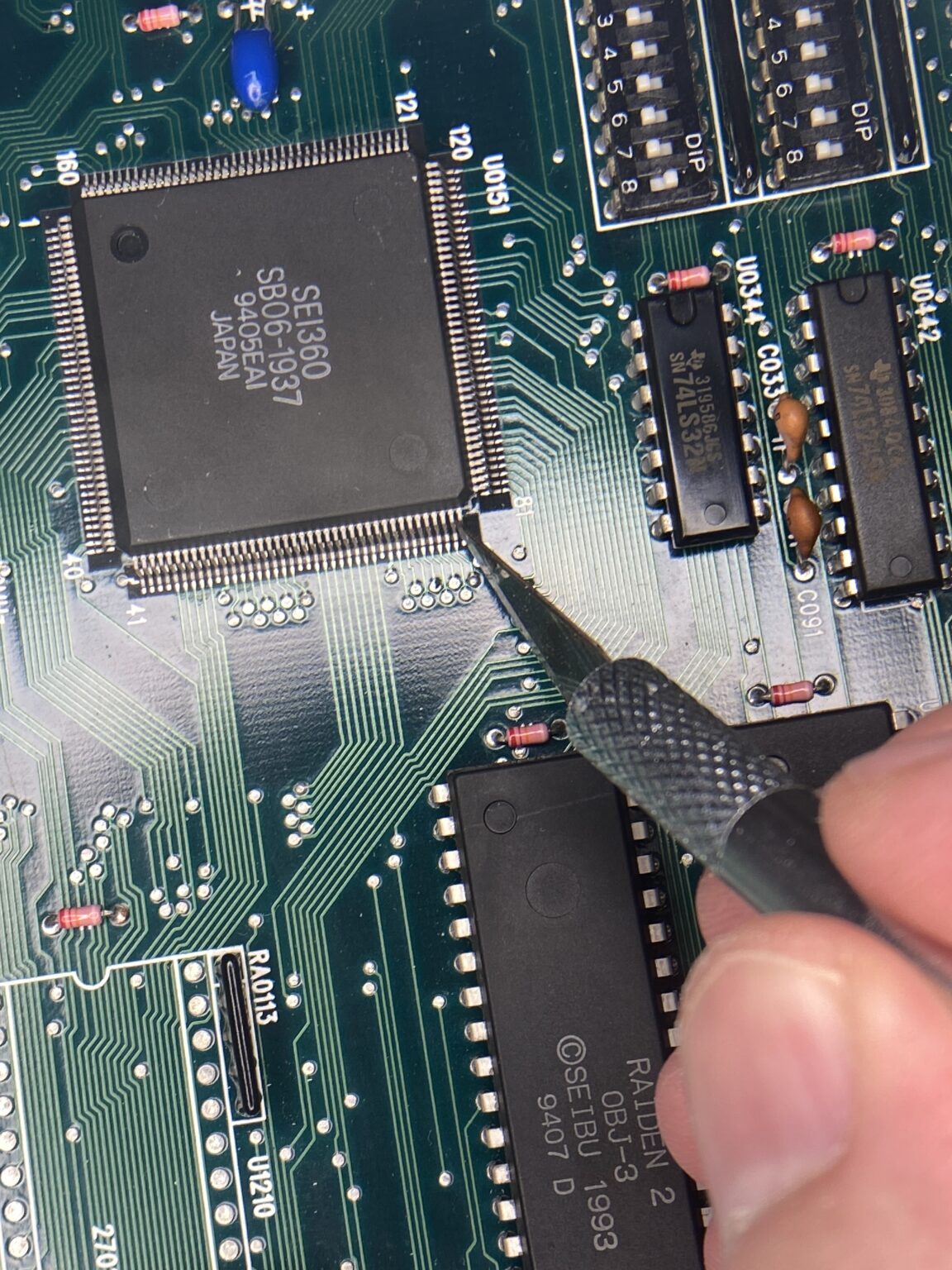
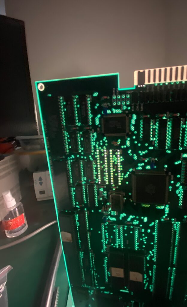
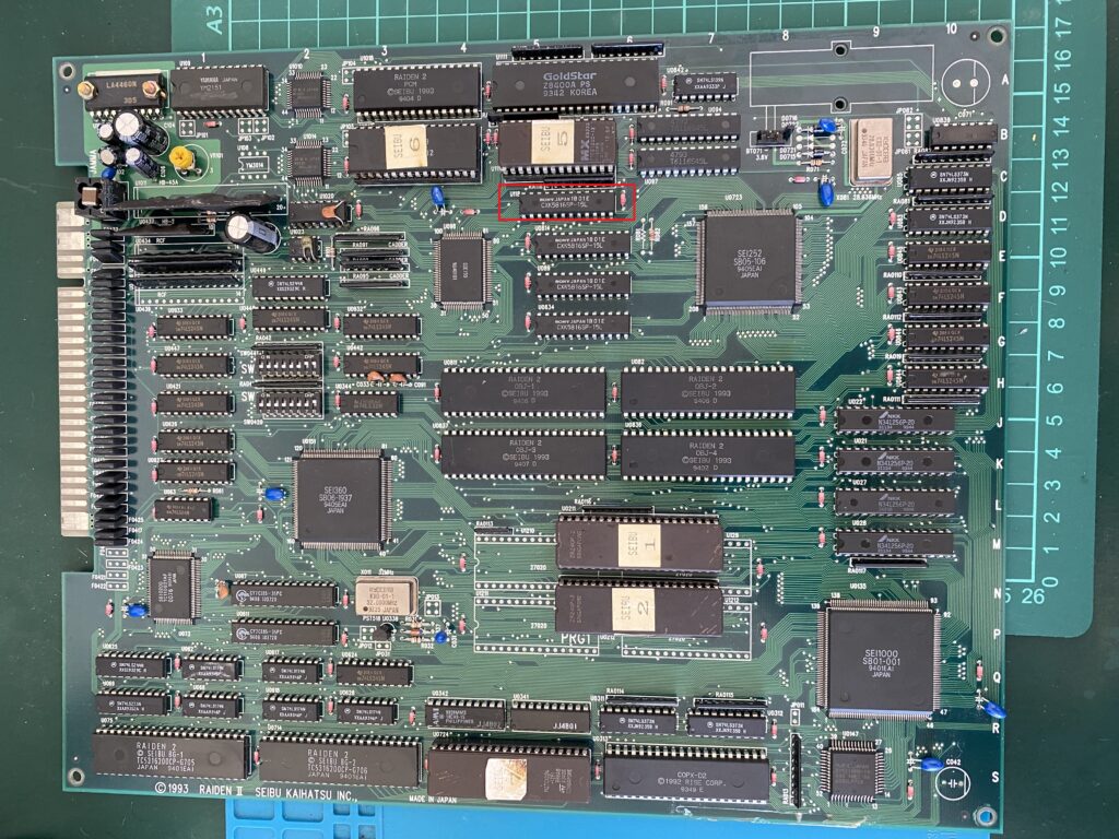
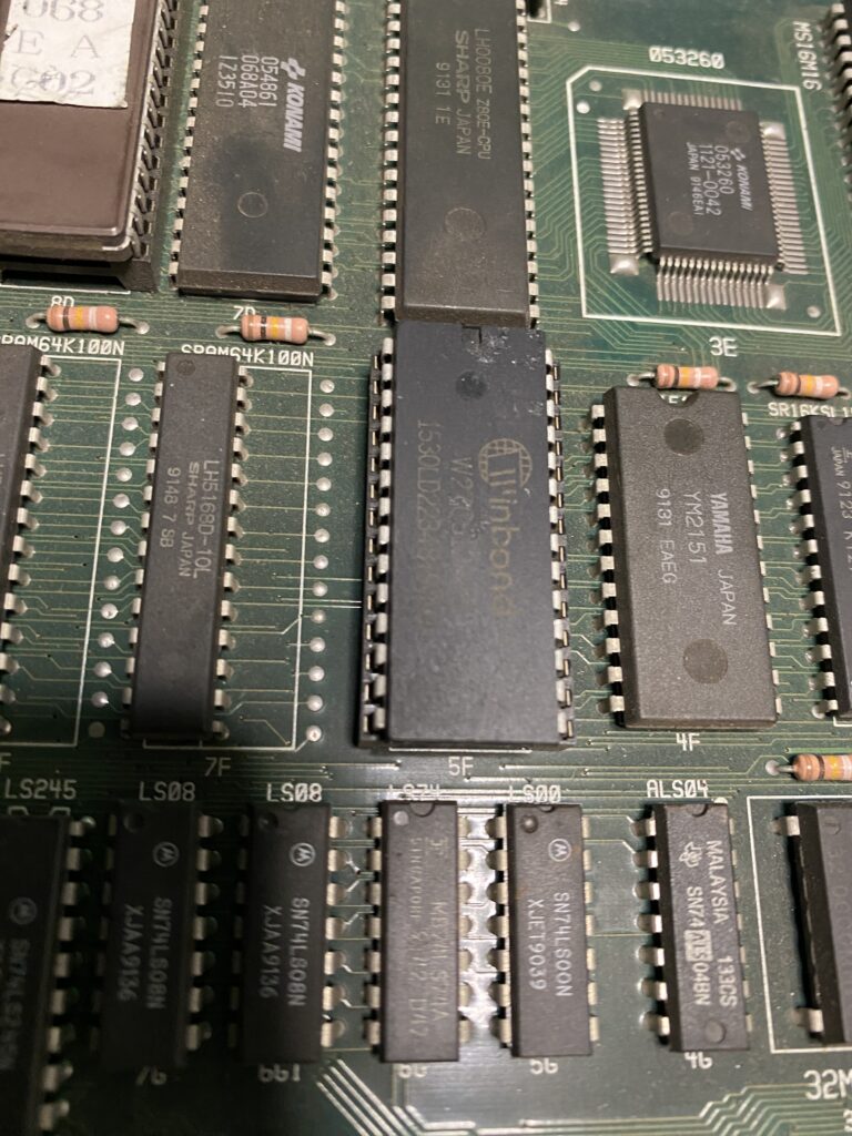
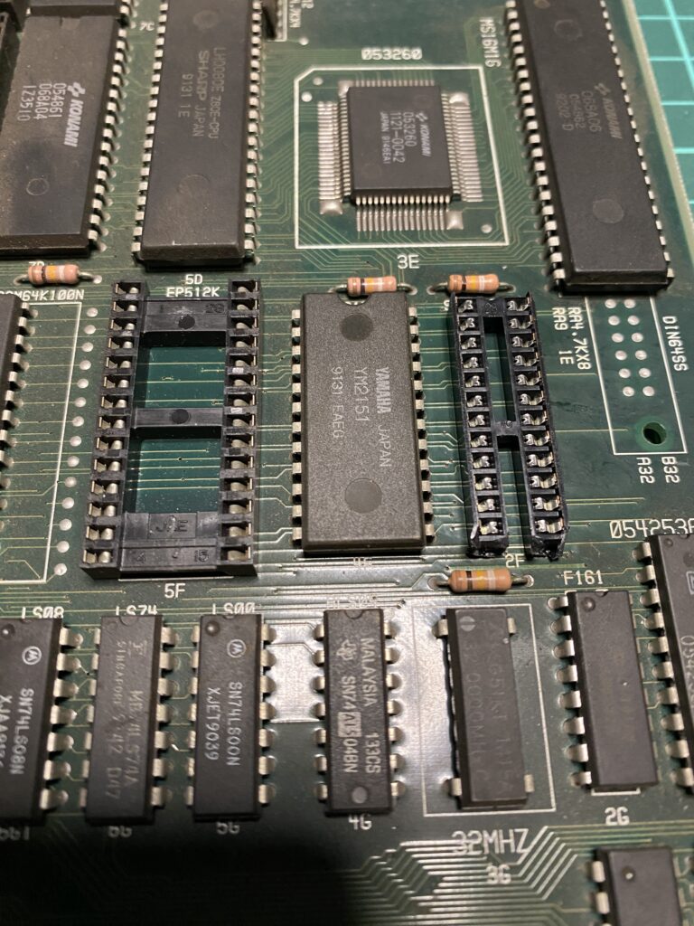
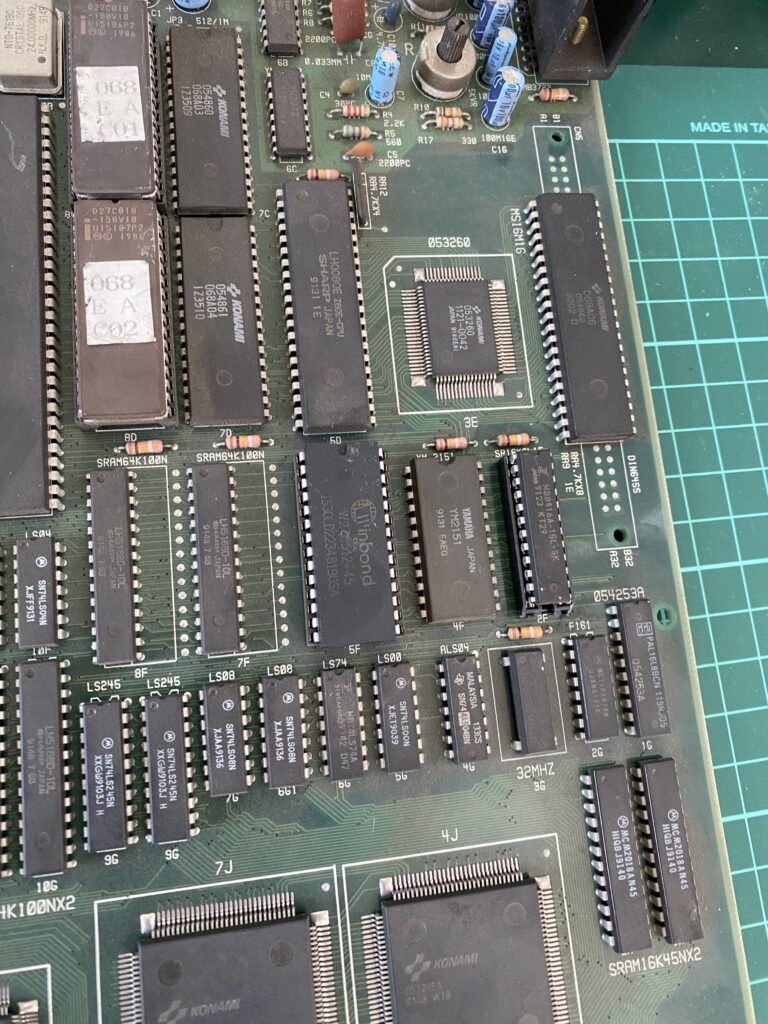
This is the board:
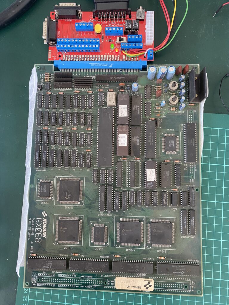
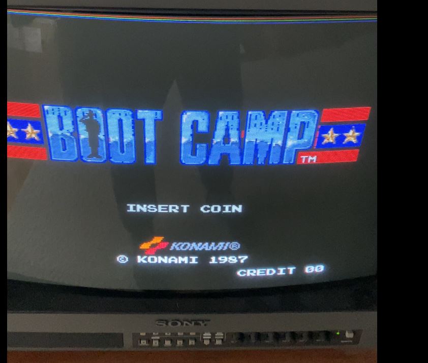
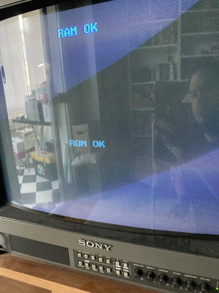
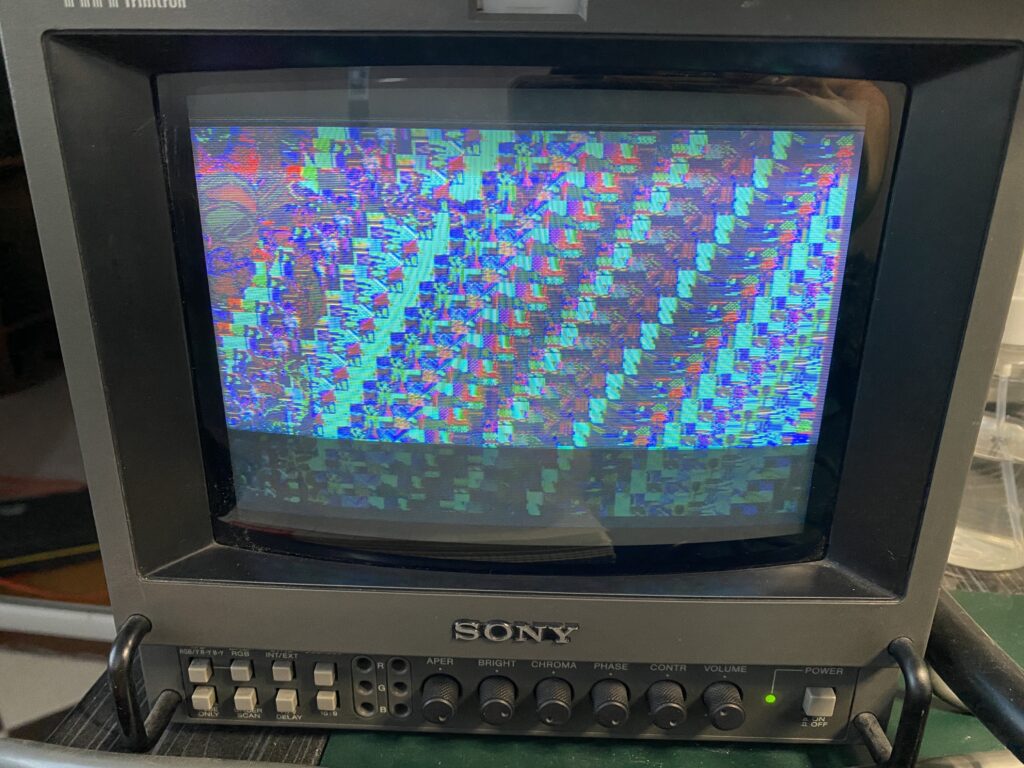
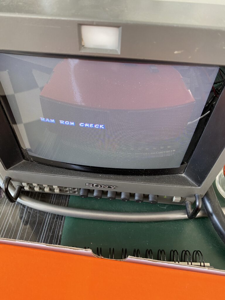
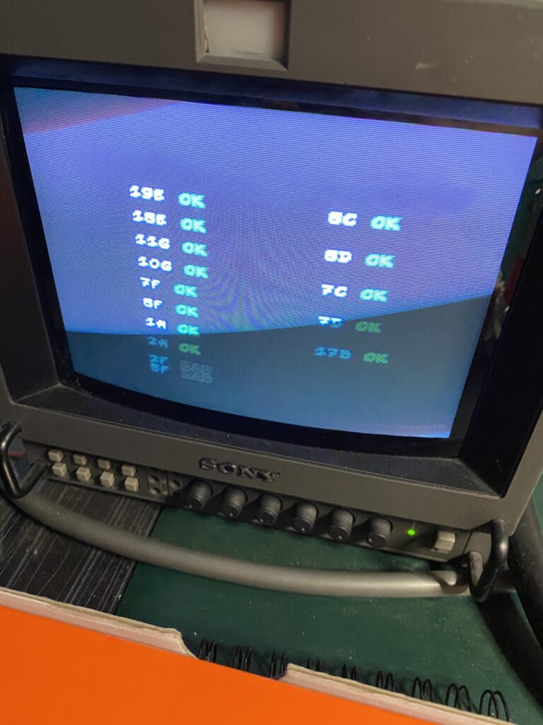
I immediately attached it to my JAMMA Test Rig and powered it up.
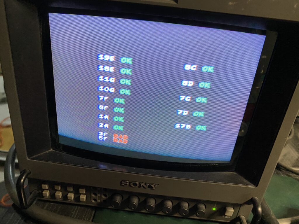
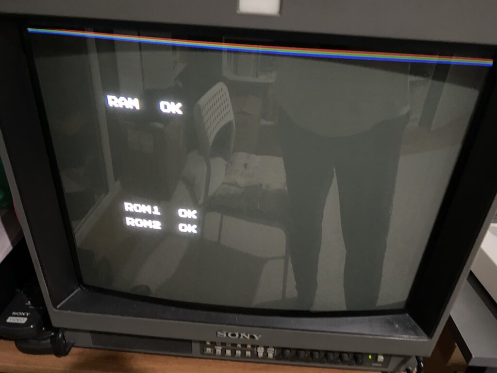
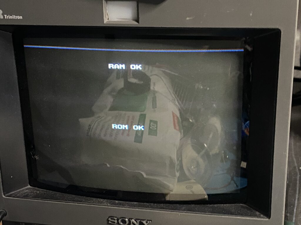
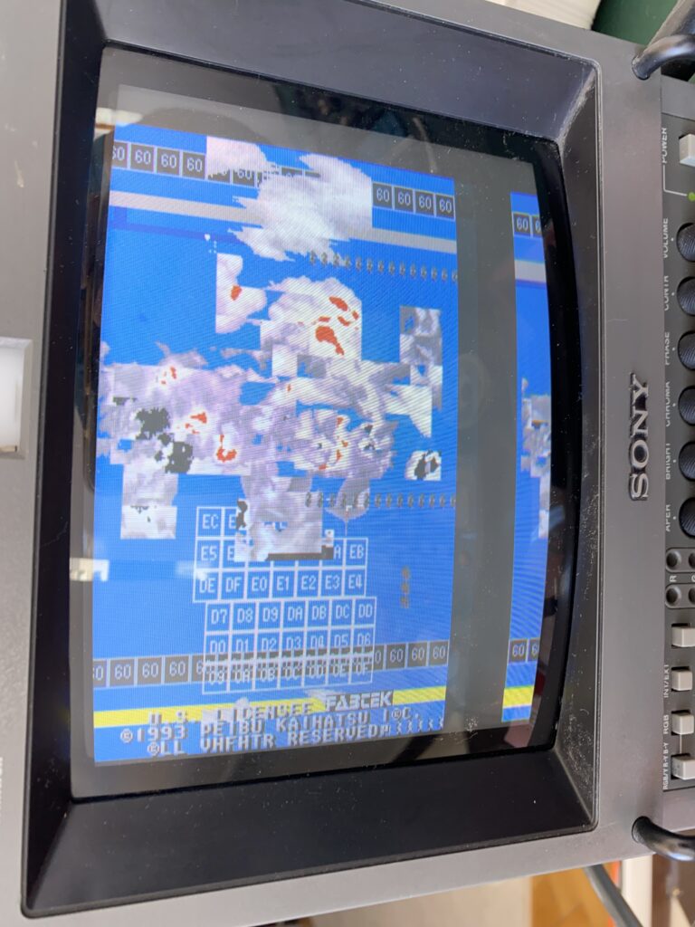
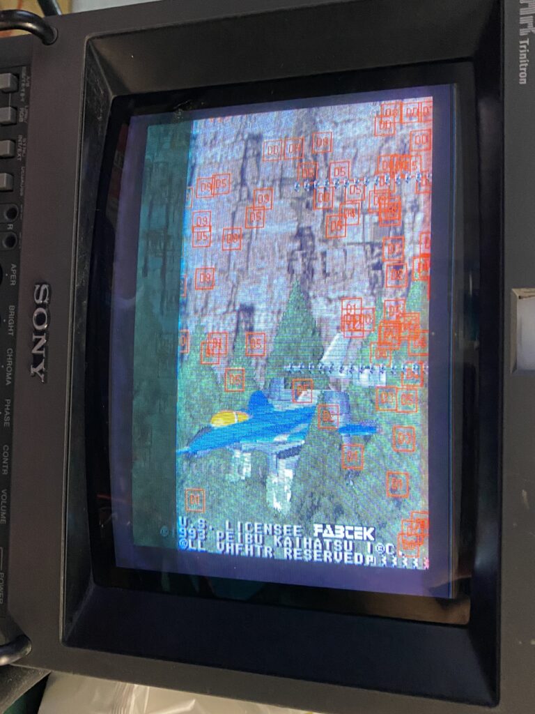
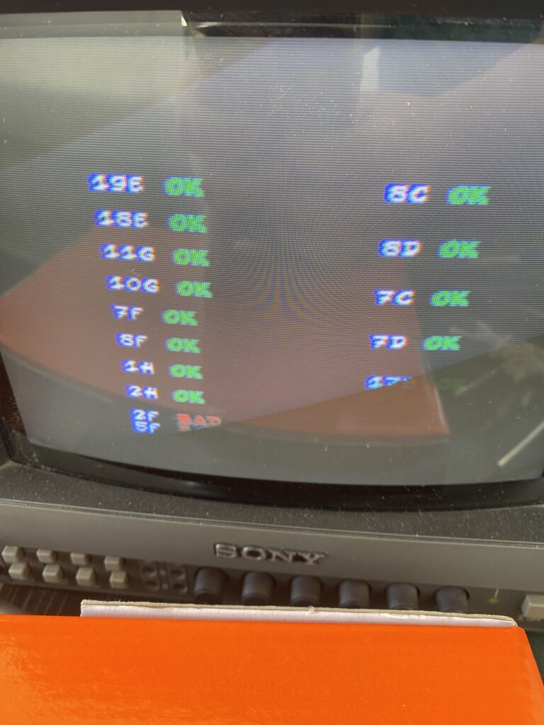
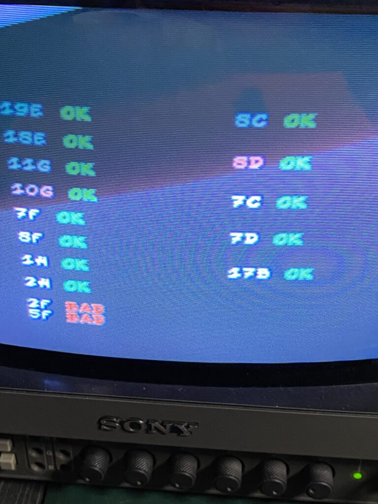
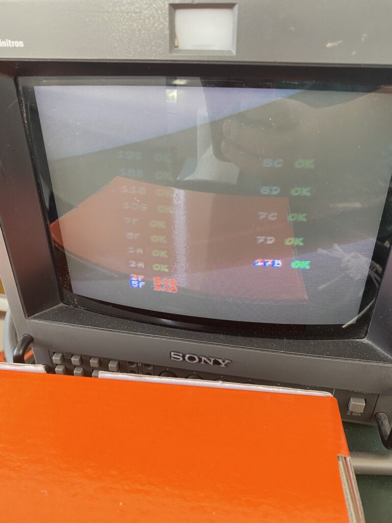
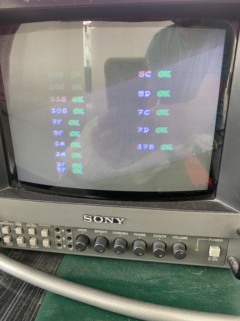
Indeed, we see 2 defective chips on the board’s ROM Check screen – 2F and 5F.
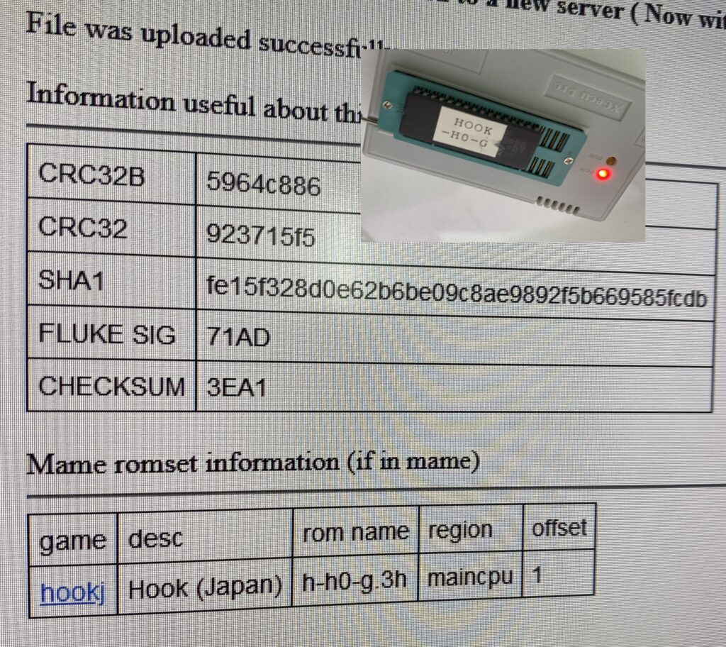
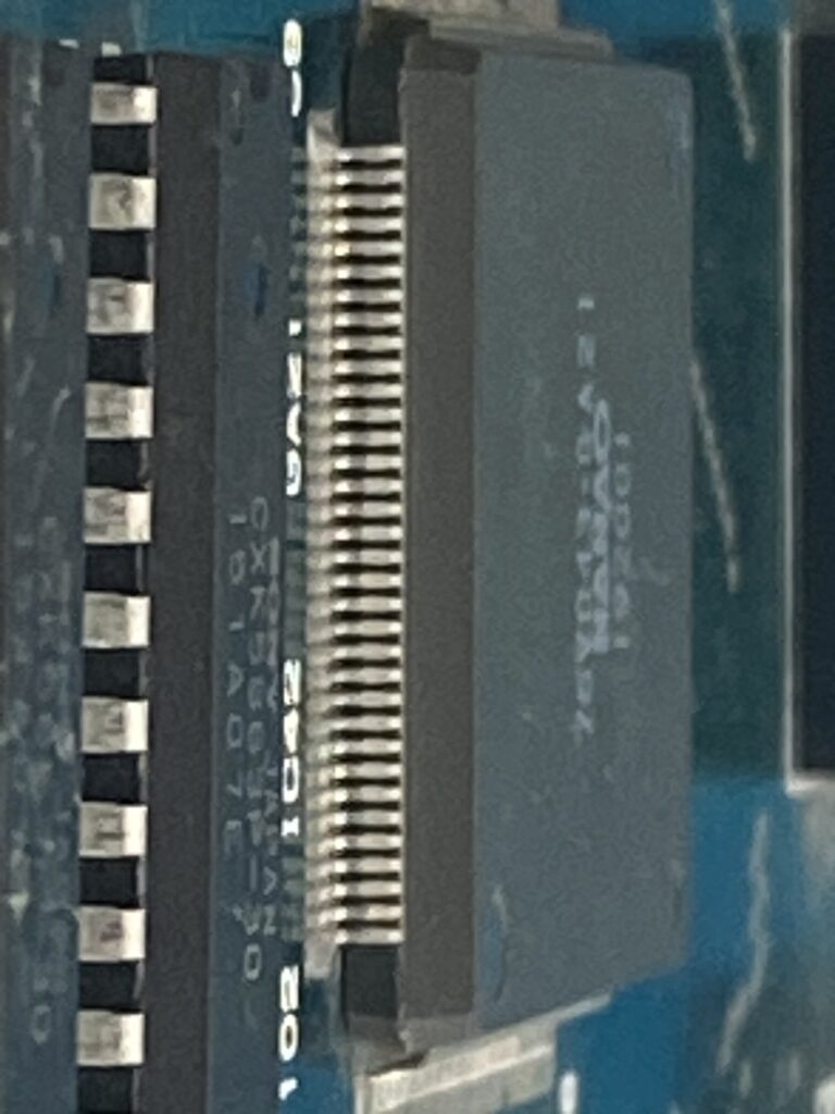
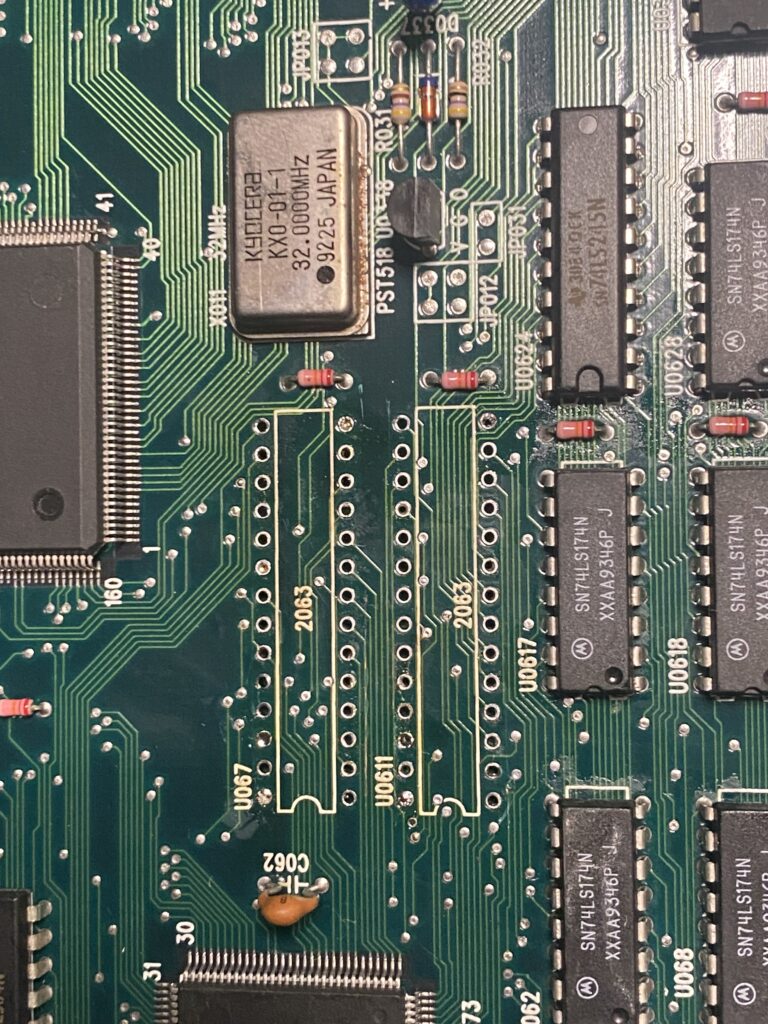
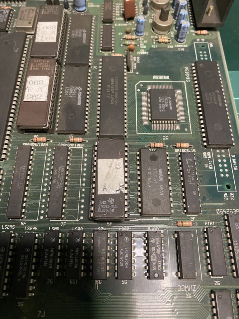
When examining the board, we see that 2F is a RAM chip while 5F is a ROM chip.
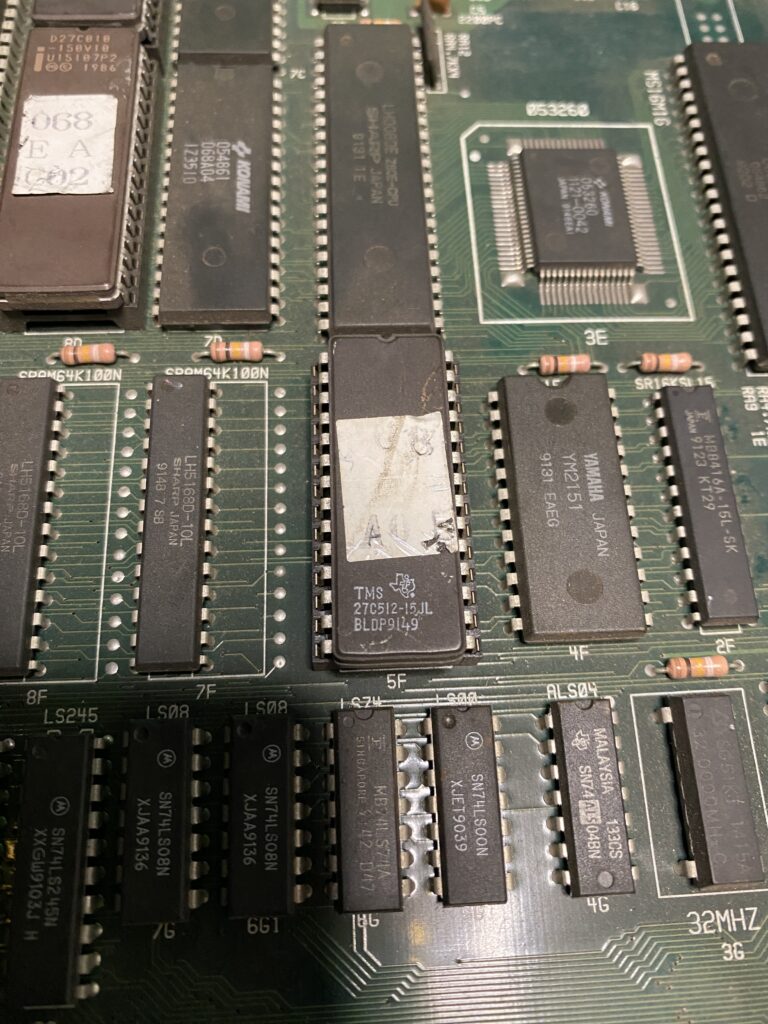
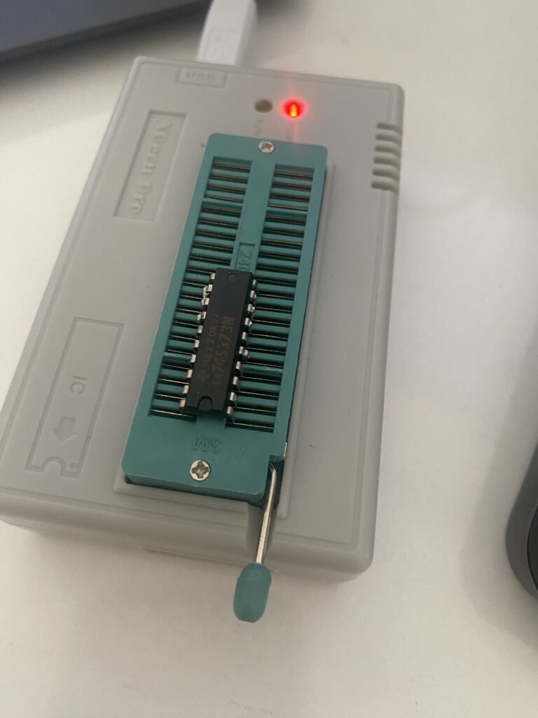
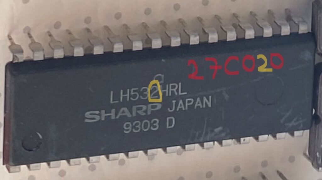
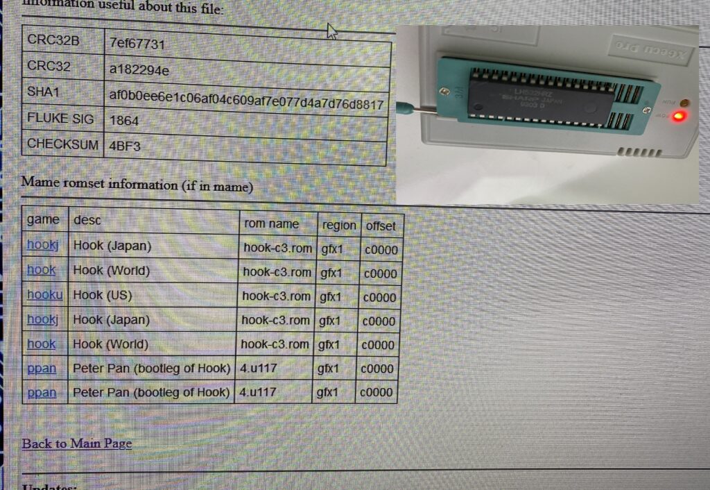
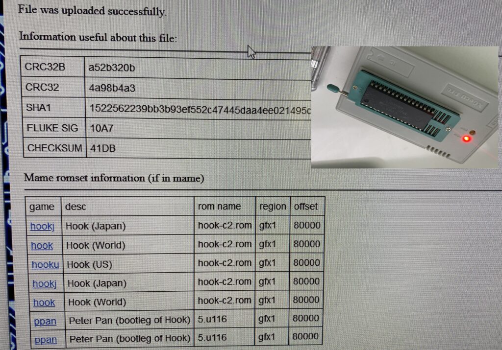
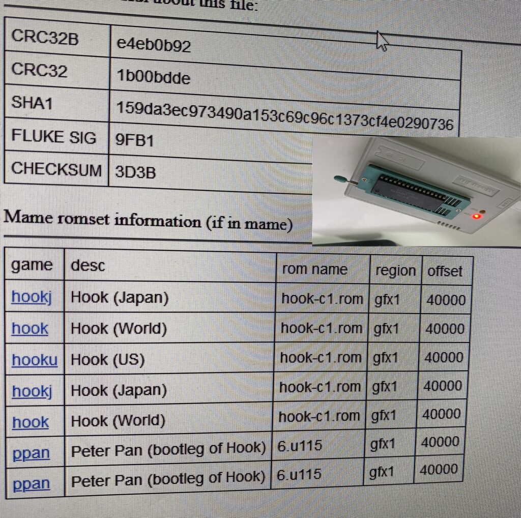
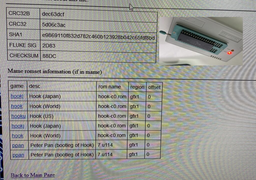
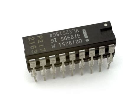
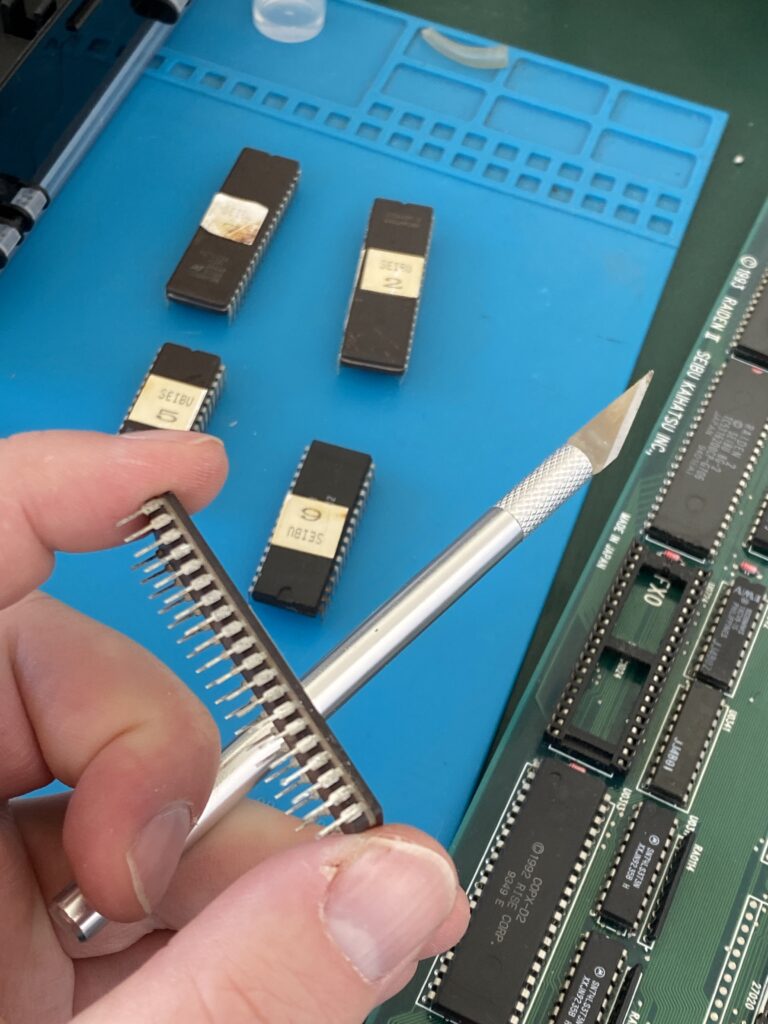
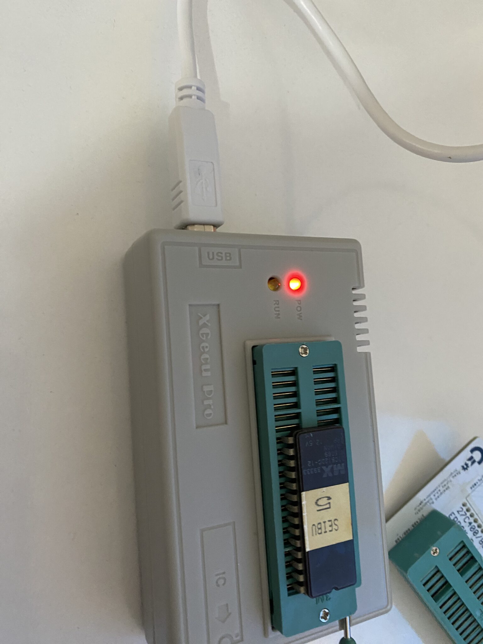
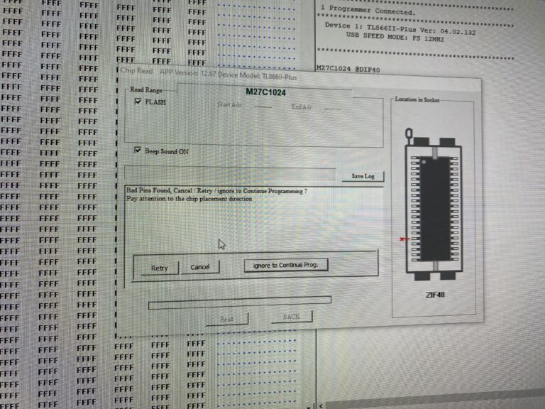
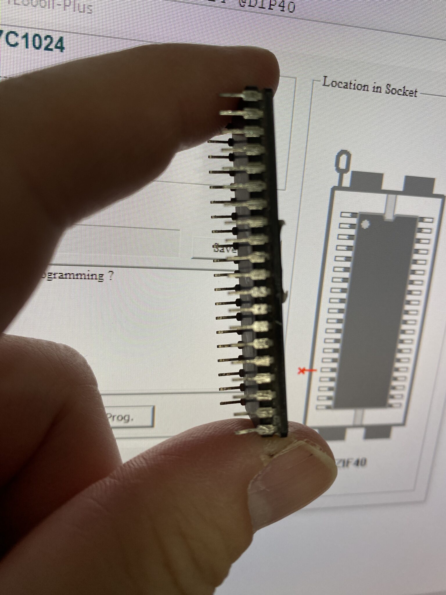
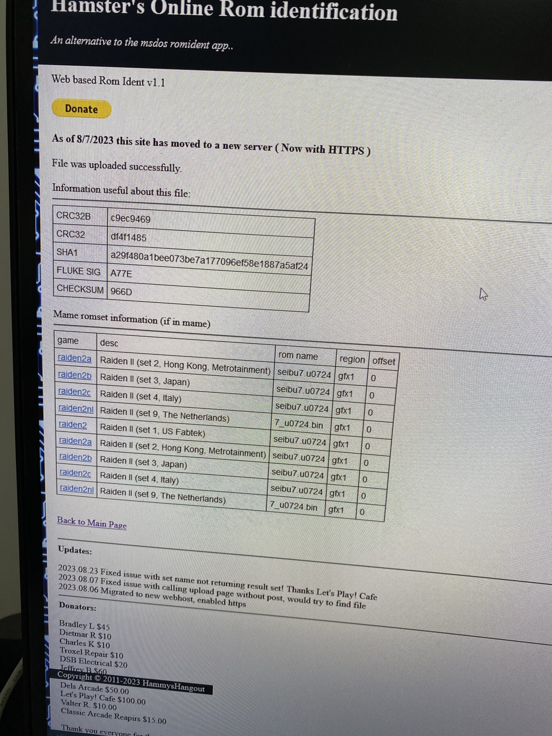
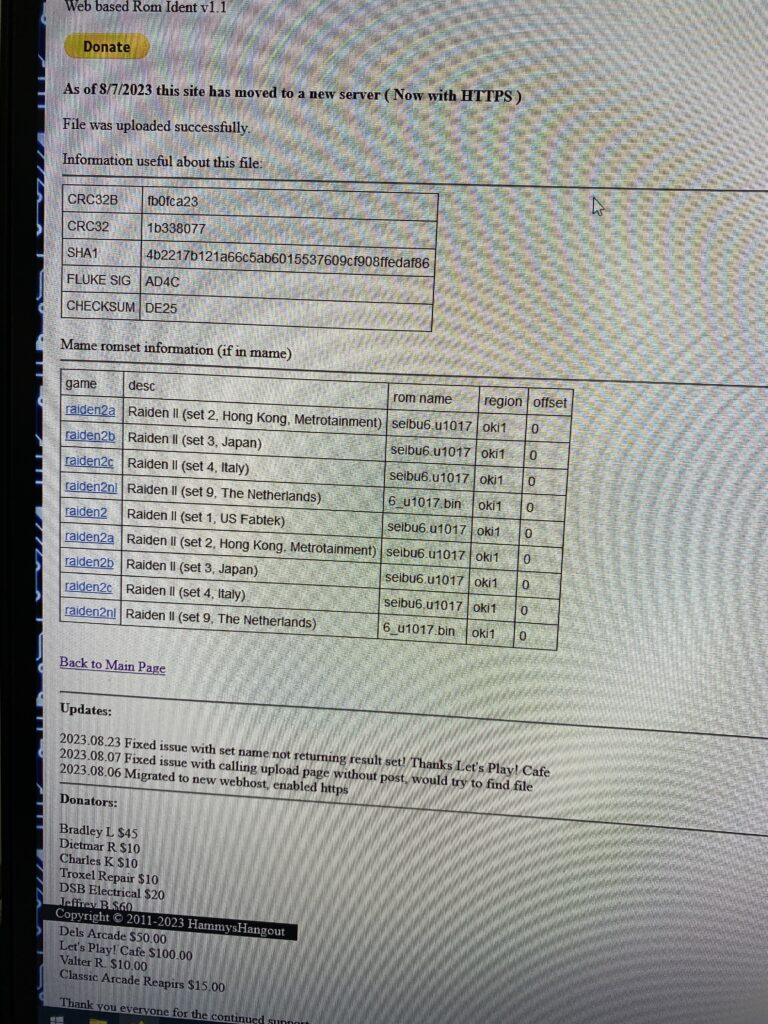
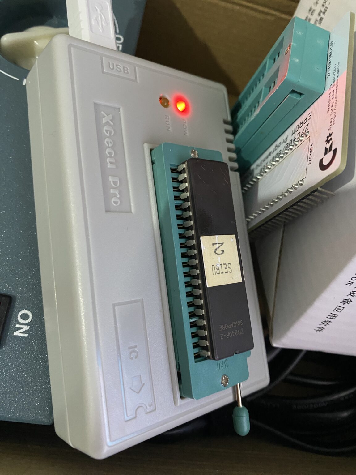
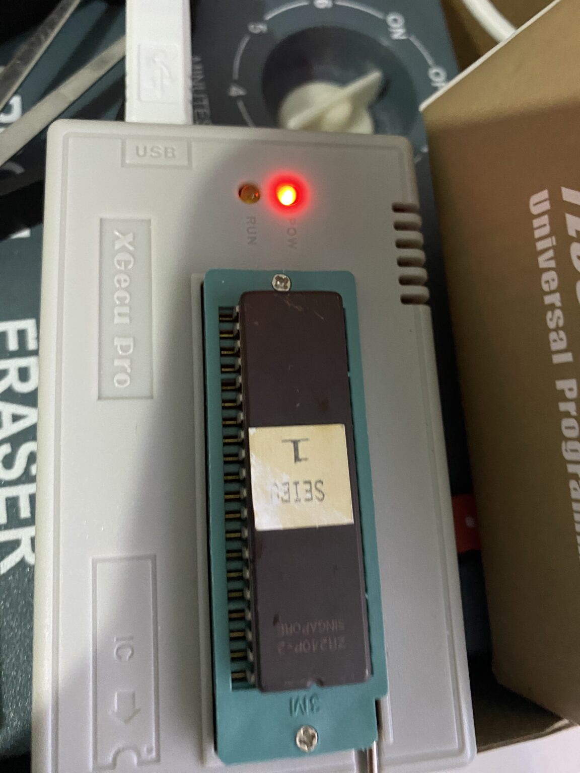
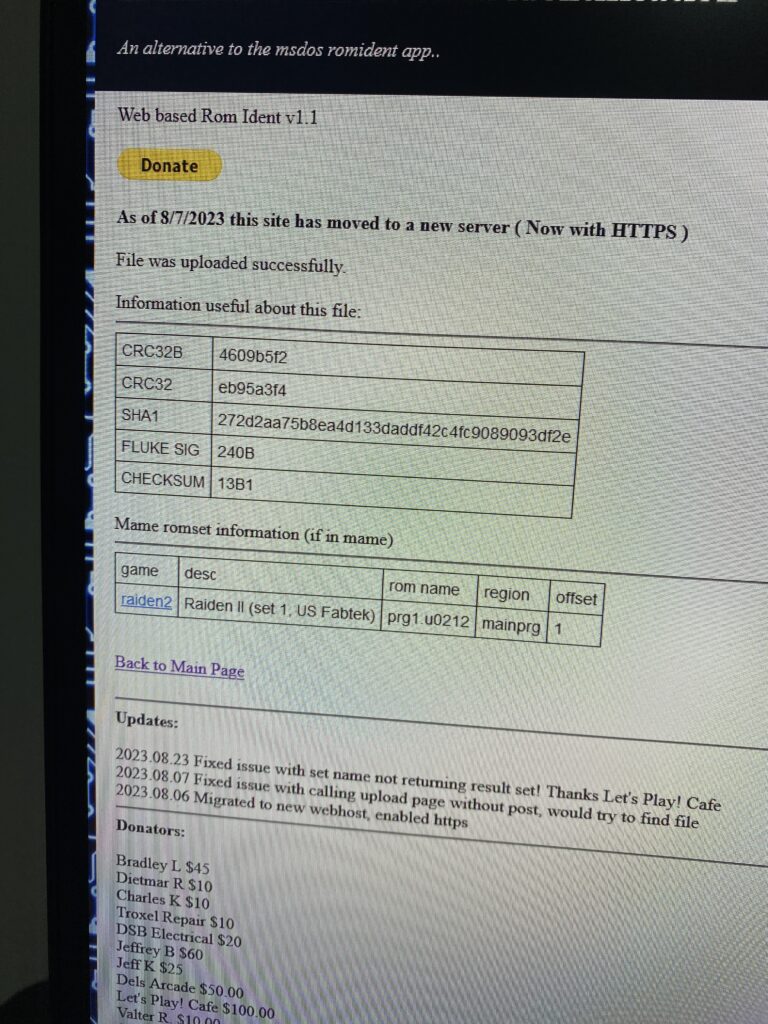
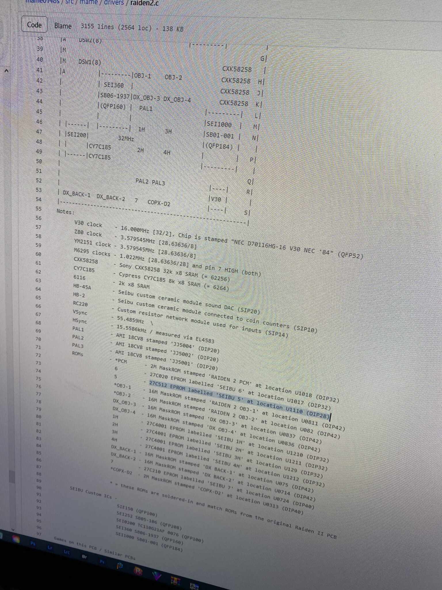
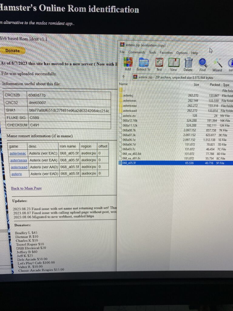
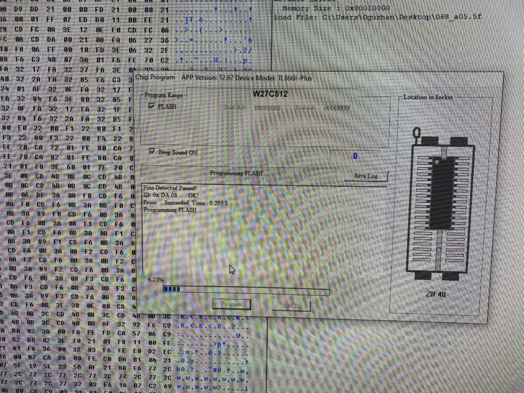
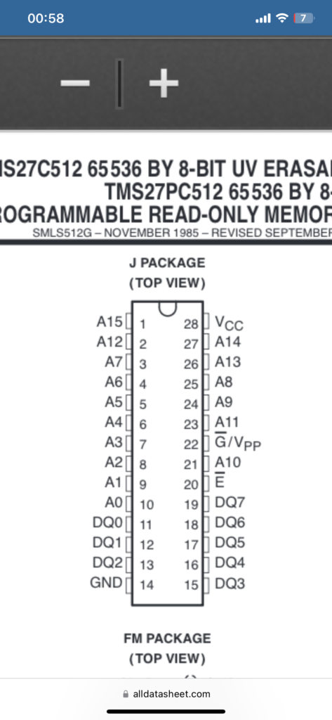
The 5F EPROM (TMS27C512) is already socketed, so let’s dump it and compare it with MAME via the ROMIdent site.
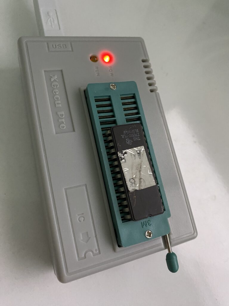
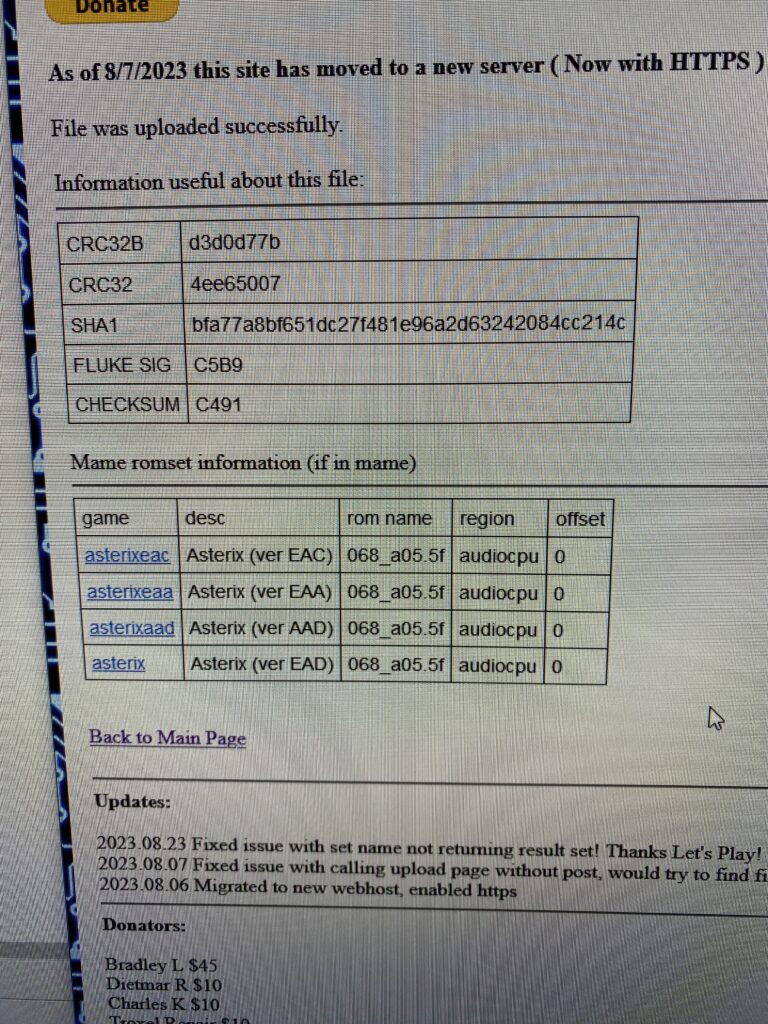
The ROM looks fine and matches what it should be. For good measure though, I’ll rewrite the dump back to the EPROM.
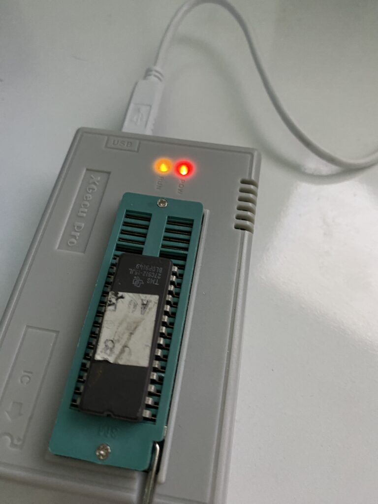
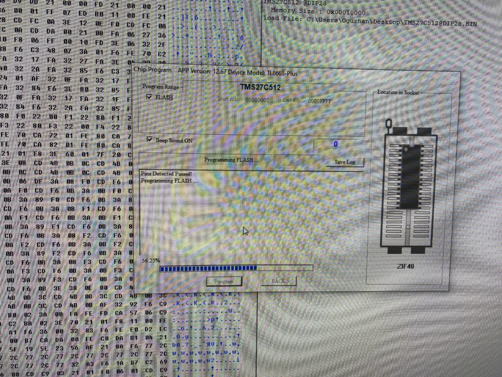
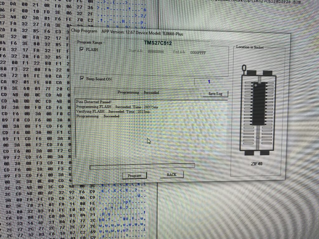
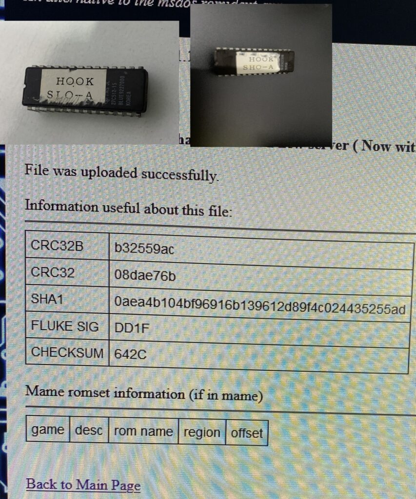
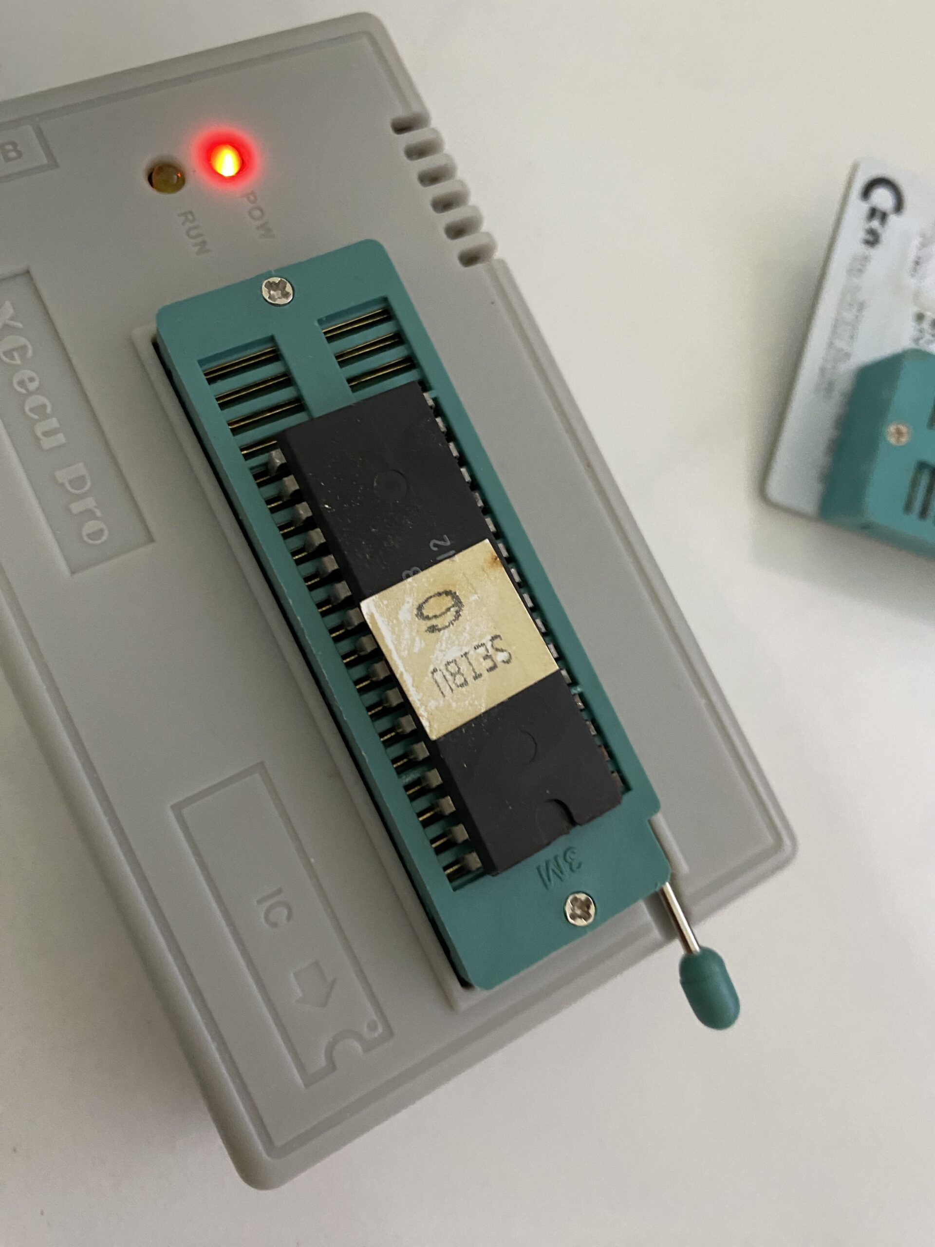
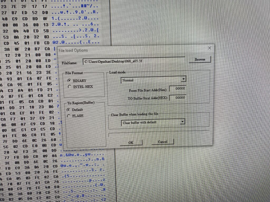
Then, while I’m at it, I’ll write the MAME equivalent dump file 068_a05.5f to another EPROM (W27C512) that I’m sure is good, so that we can try both.
First, I’ll put the old ROM back in and try it out.
Let me give you some information if you try a similar experiment. With some Konami boards, if you change ROM chips, the system might not detect it. For example, when switching from a 2P ROM to 4P ROM, or switching to a different language ROM.
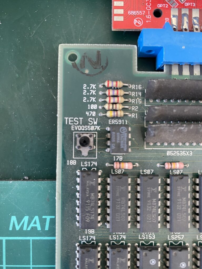
If this occurs, hold down the TEST SW button while powering on the board. You should see an EEPROM Initialization message.
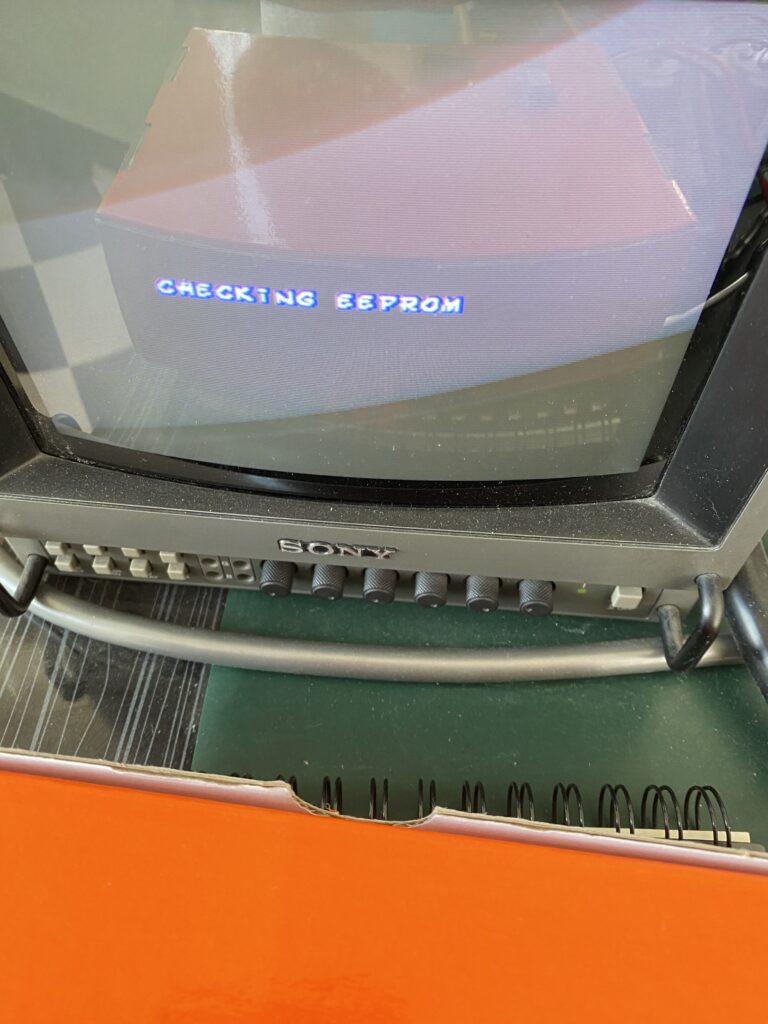
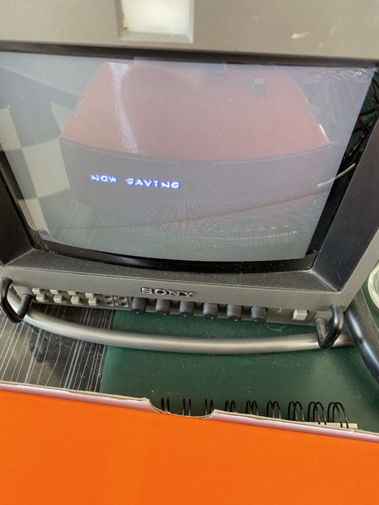
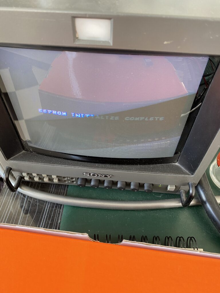
After the EEPROM reinitializes, it goes into the normal boot routine. Let’s see if 5F is fixed.
Not yet! Let’s try the new EPROM I wrote in case the old part is faulty.
It’s still not fixed. For now, let’s leave all this aside and deal with the RAM. Maybe problematic RAM is also causing problems accessing the ROM.
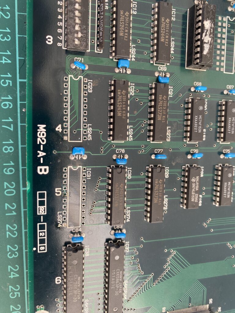
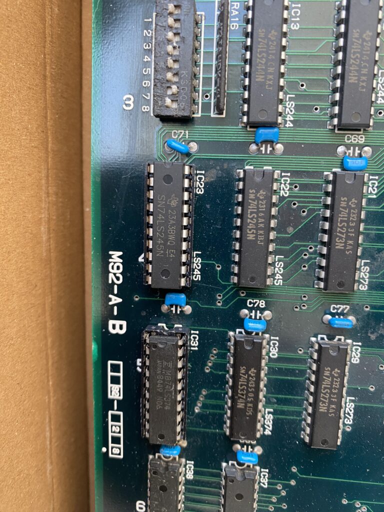
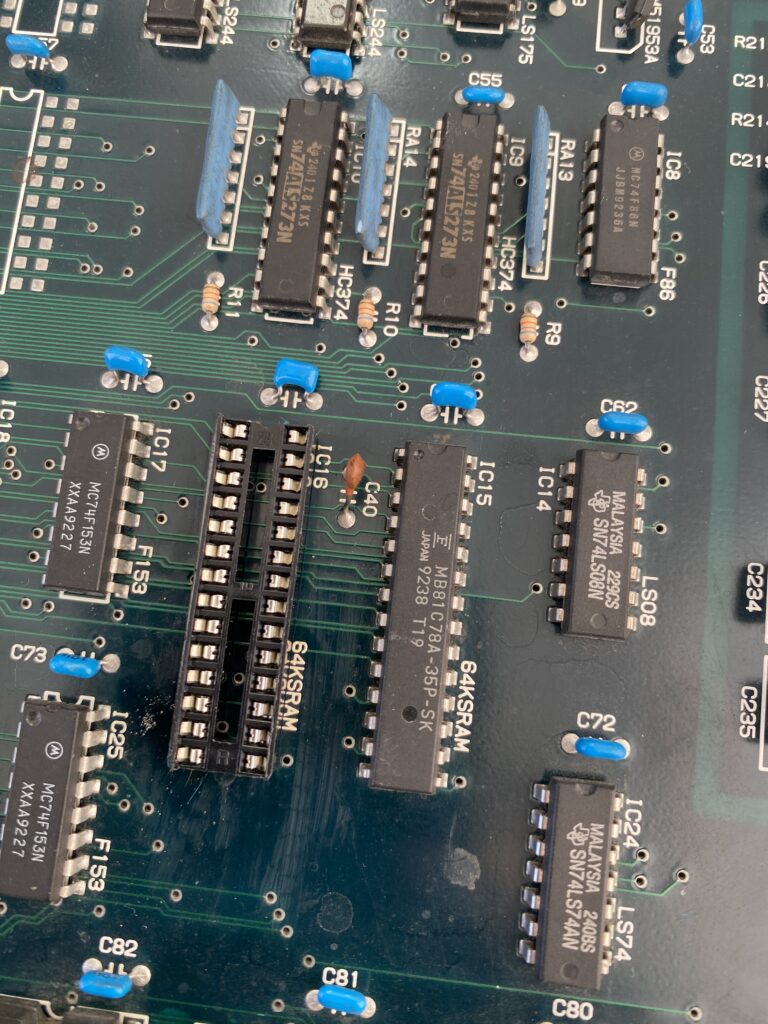
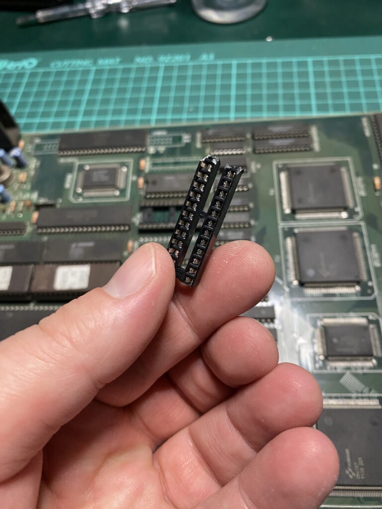
I carefully remove the old RAM by desoldering it from the board.
I’m out of suitable sockets for that pinout, so I cut down a large socket. It’s not fantastic but it does work!
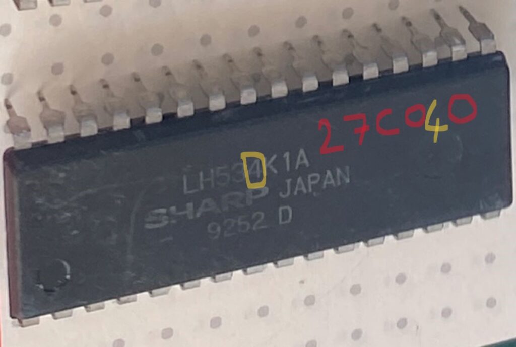
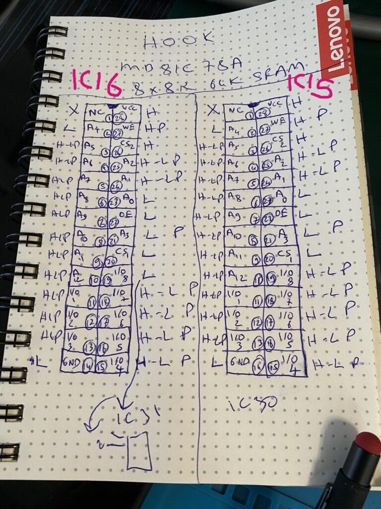
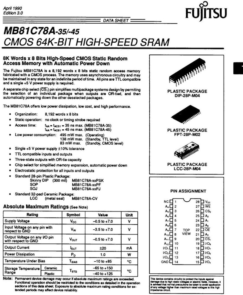
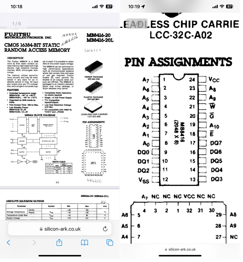
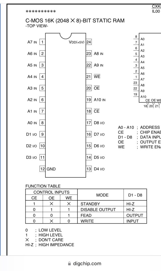
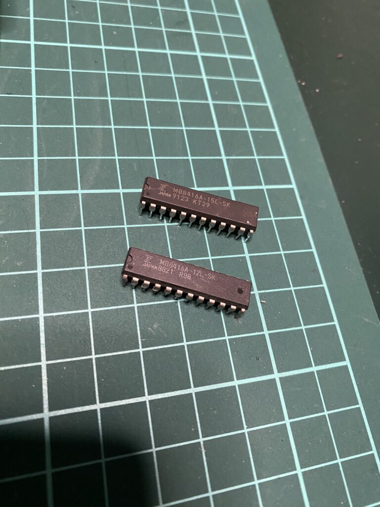
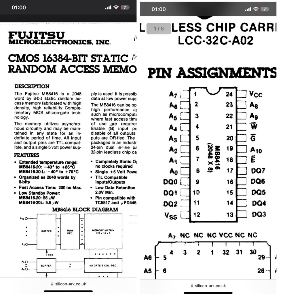
The part number of the RAM that came out of the board is MB8416A-15L-SK. I have a similar part that I can put in its place – MB8416A-12L-SK. The 12 means 12ns, i.e. shorter access time, i.e. faster RAM.
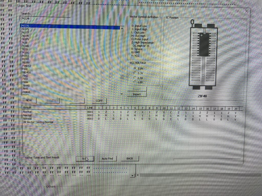
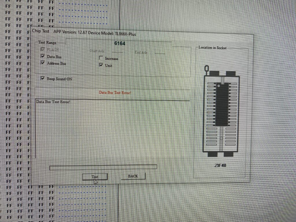
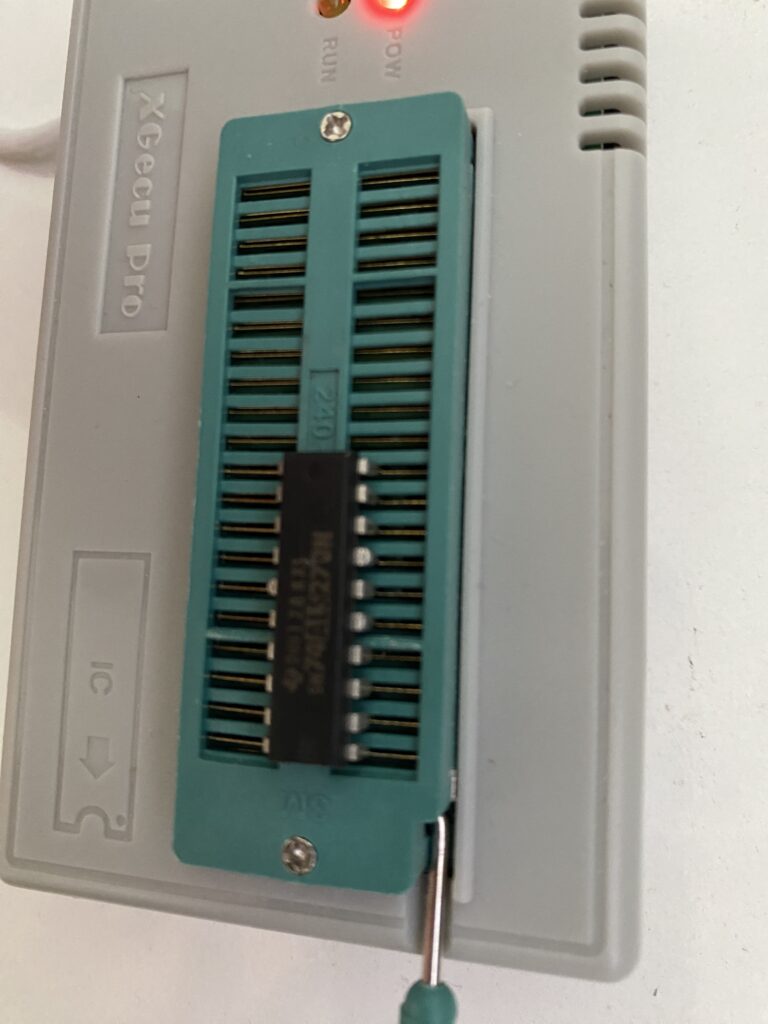
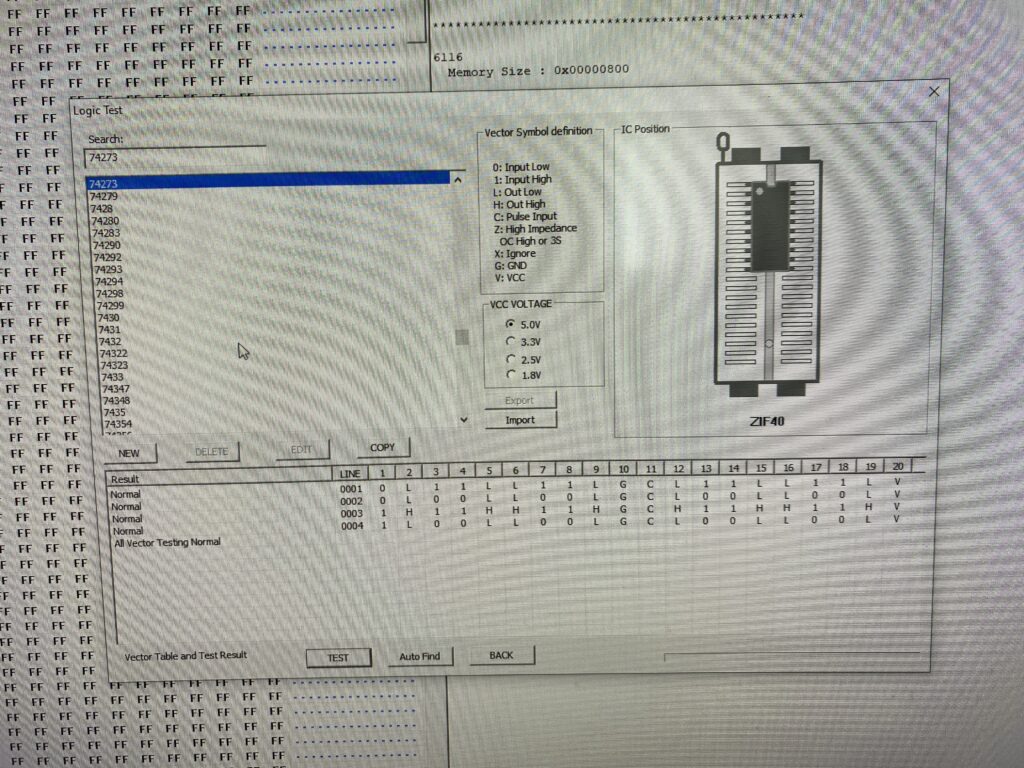
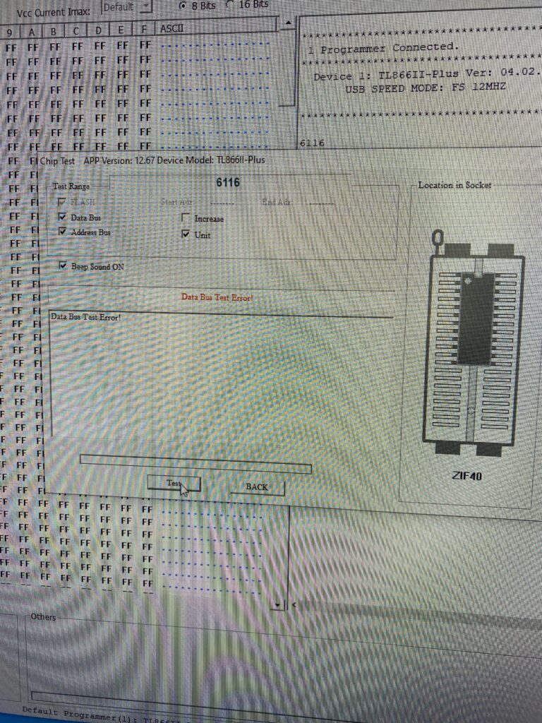
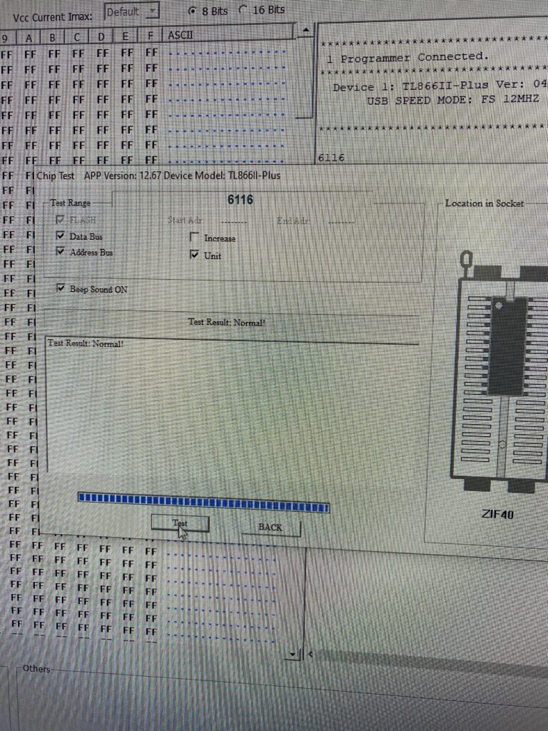
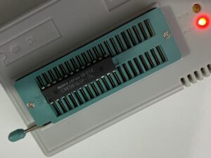
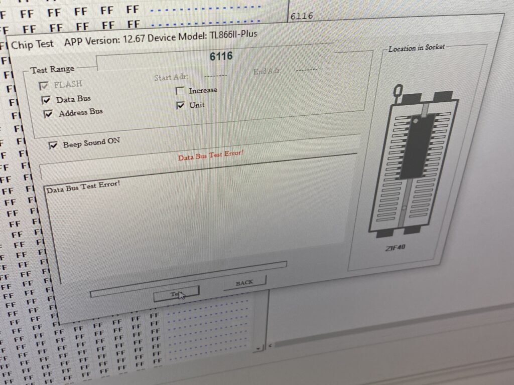
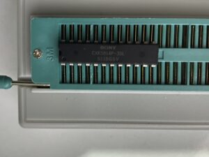
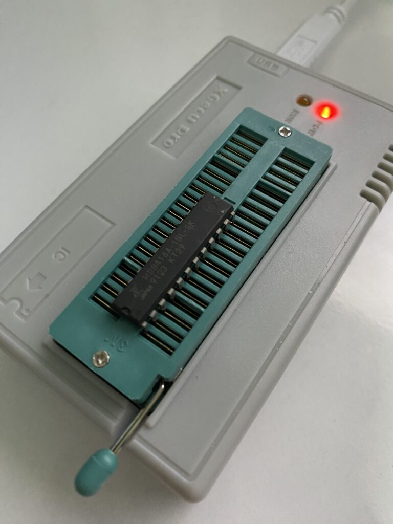
First, lets test the old RAM out of circuit with my EPROM programmer.
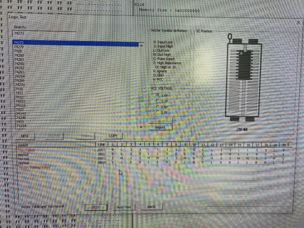
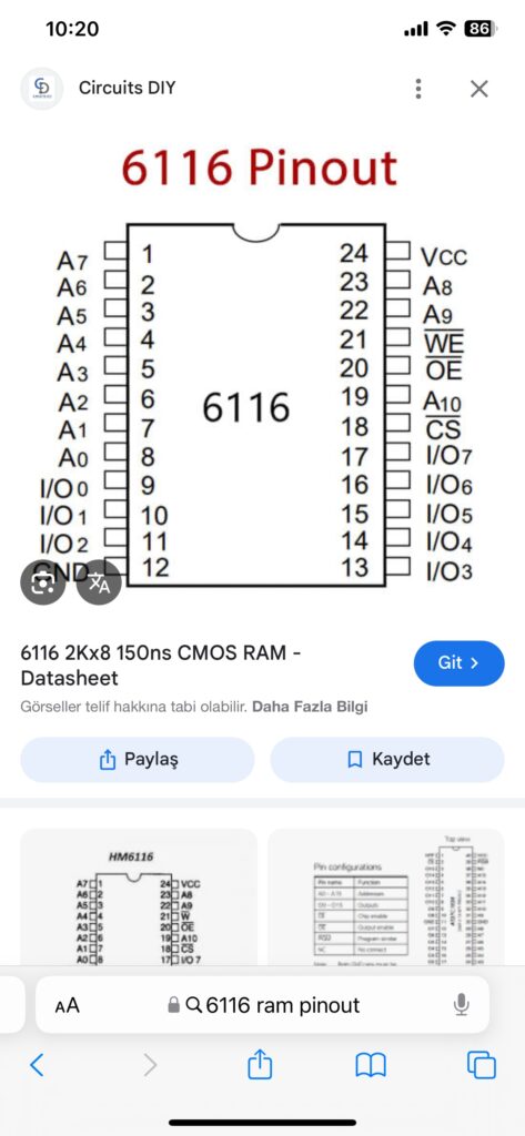
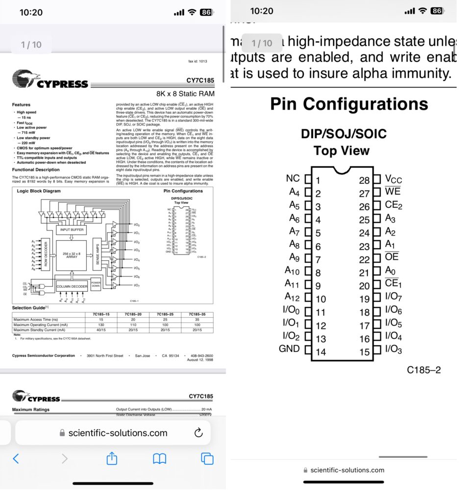
This RAM is a 6116 series equivalent. There are various cross reference sites to see equivalents. Or you can compare two datasheets and look; if you do this, pay attention to both the pinout and memory layout.
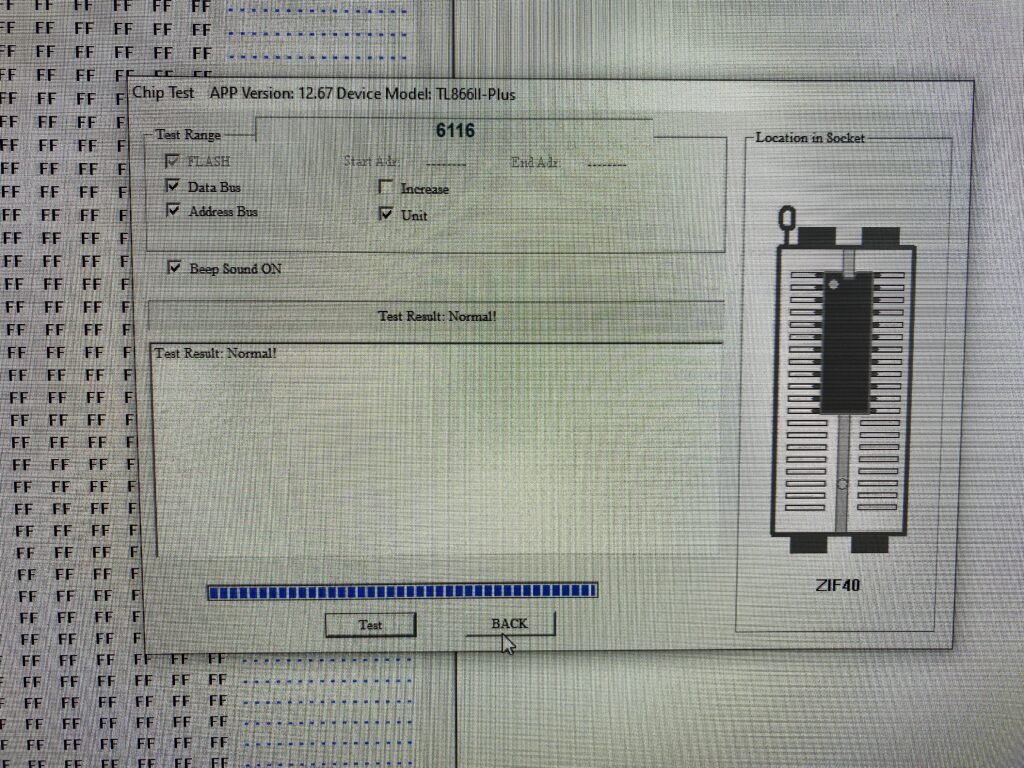
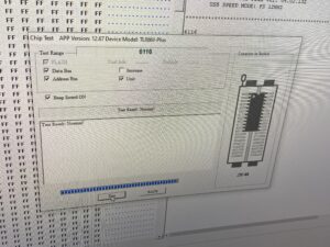
Test Result: Normal. The only time I regret that something is intact is when I’m repairing something and I suspect that the component is faulty. I wish it was faulty so I could just replace it and have it work!
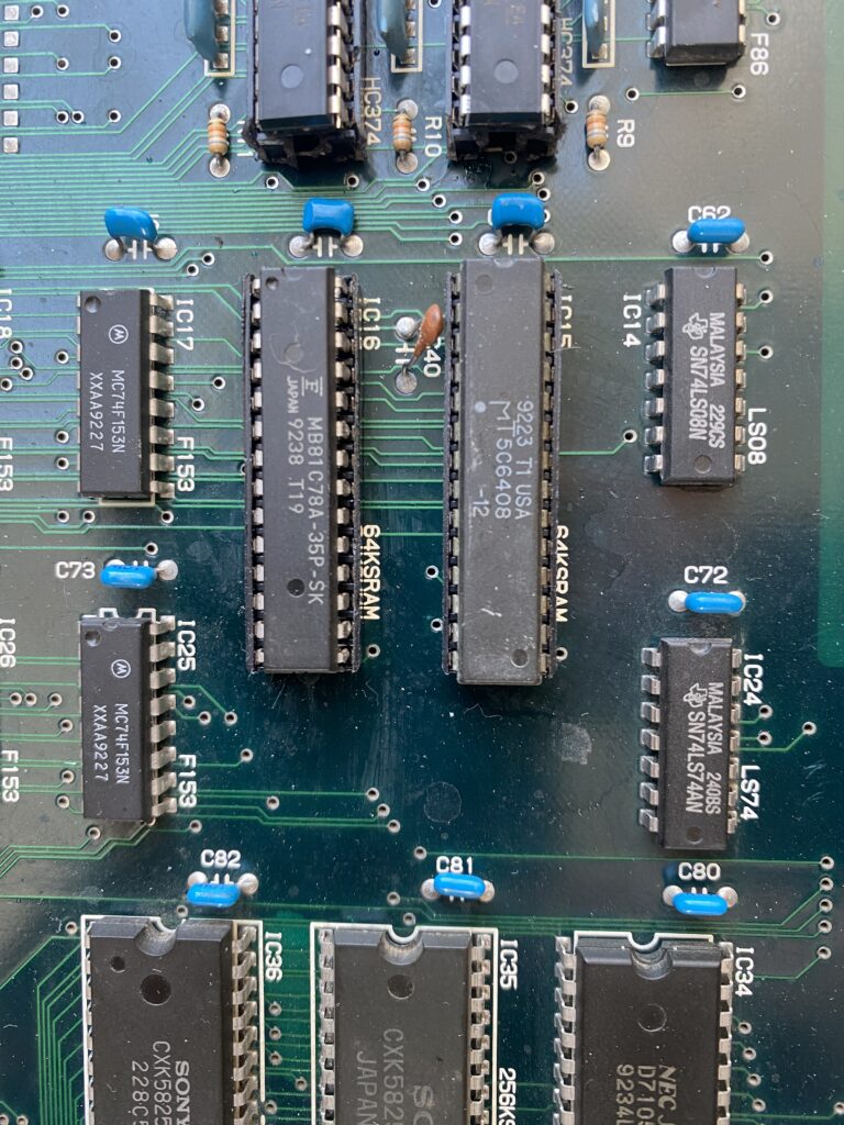
Anyway, let’s install the new RAM into the socket and boot up the game board. Sometimes out of circuit test results can be inconsistent…
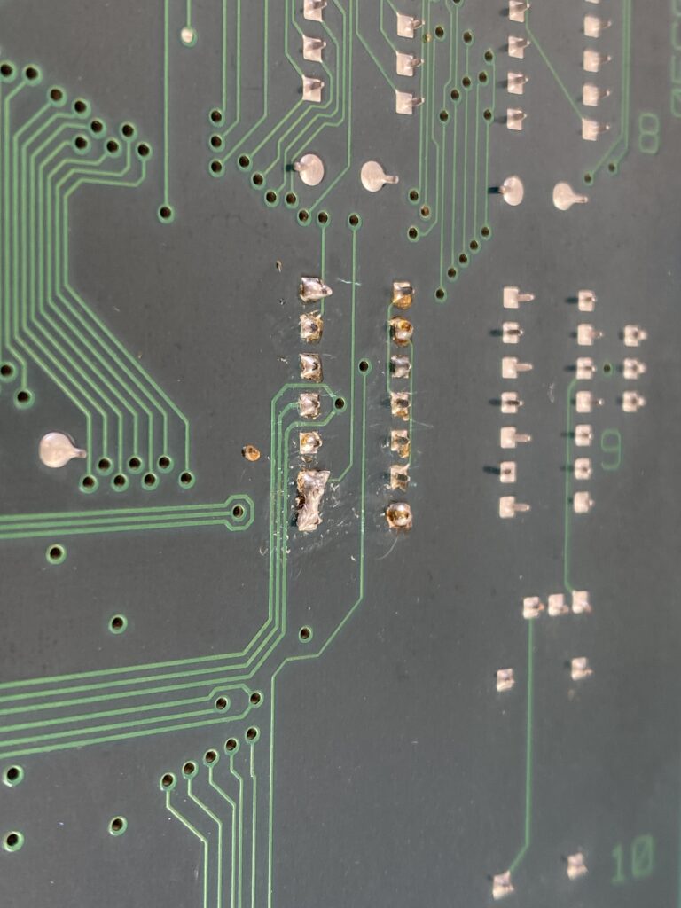
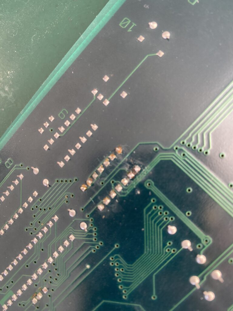
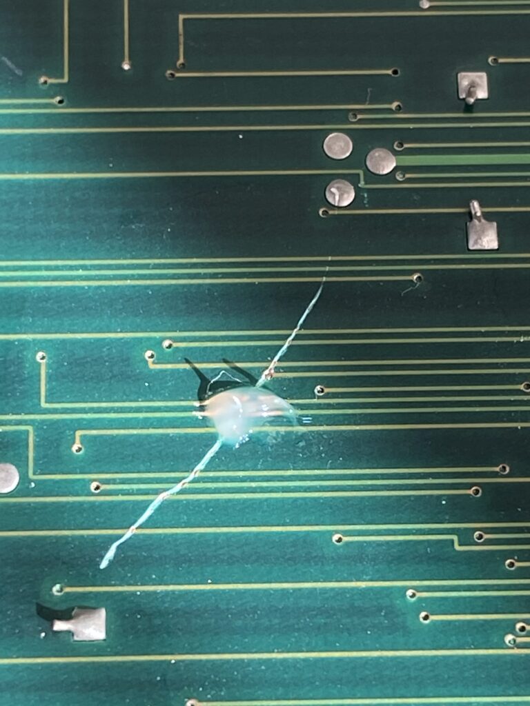
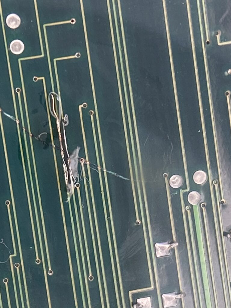
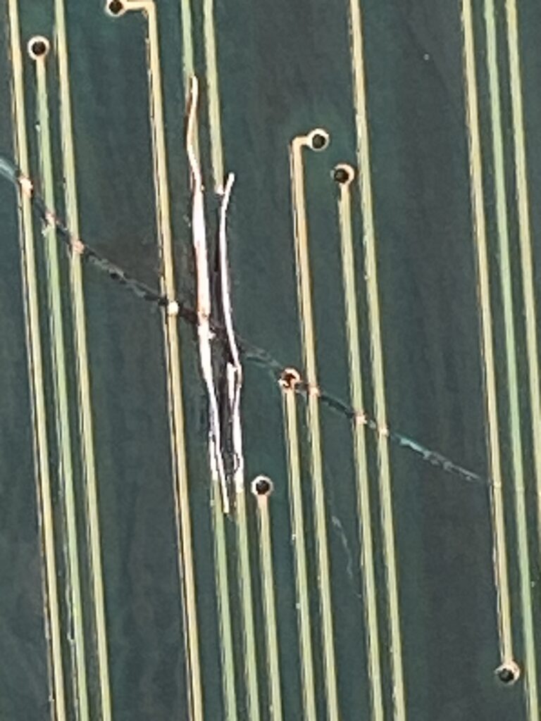
Hmmm, the 2F and 5F chips are still marked BAD so things are complicated. Apparently neither the ROM or the RAM is the problem. But somehow these two can’t be accessed correctly by the CPU. When examining the board for physical damage, I didn’t see any broken wires on the board. I didn’t see any cold solder.
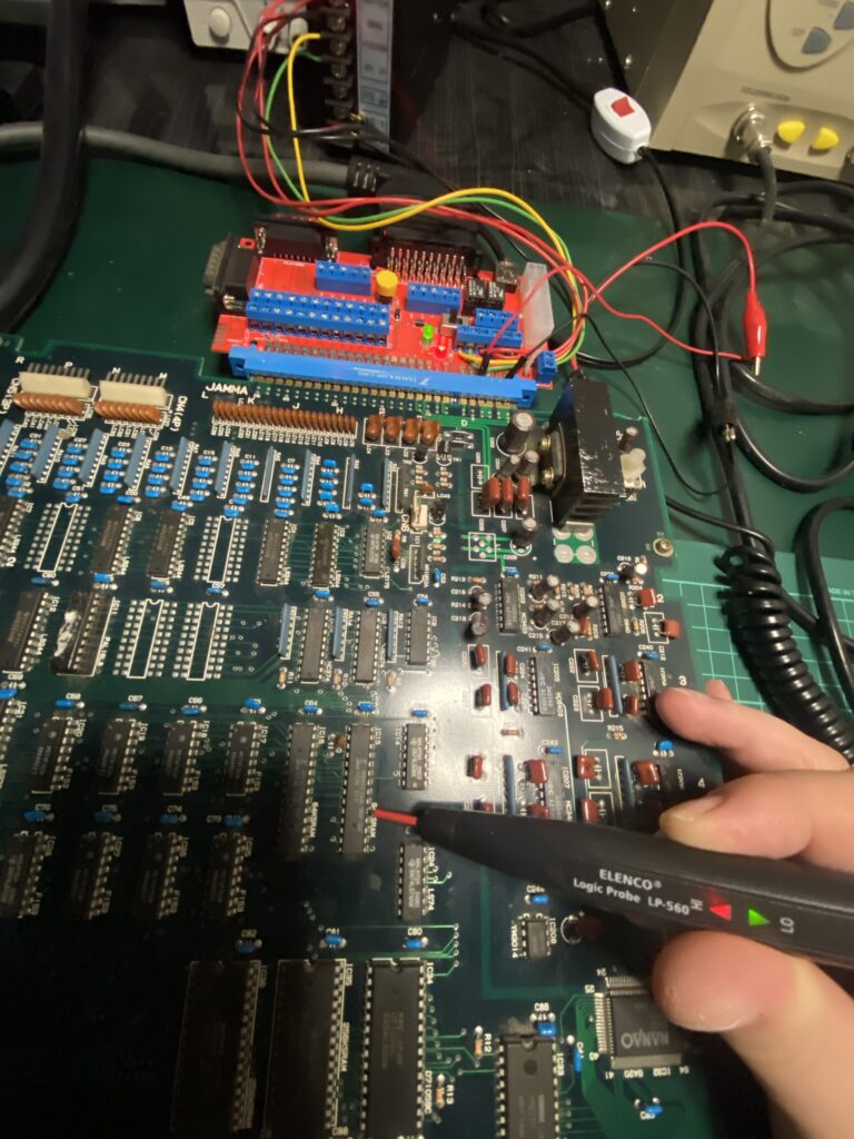
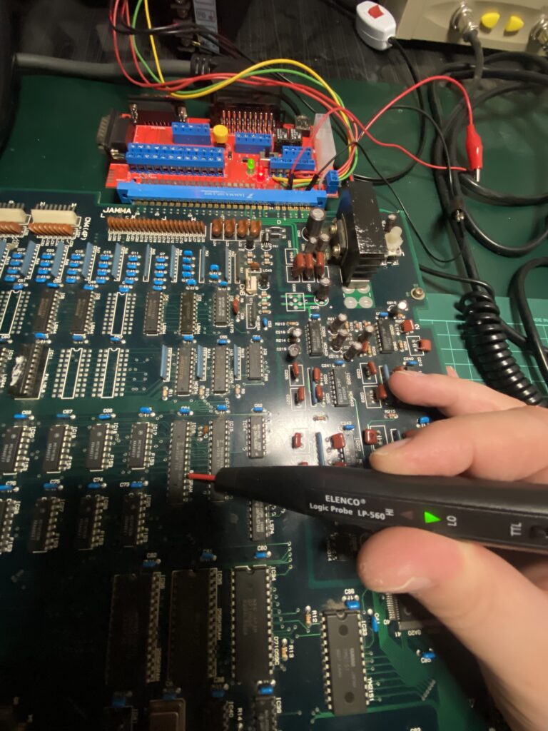
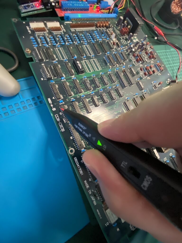
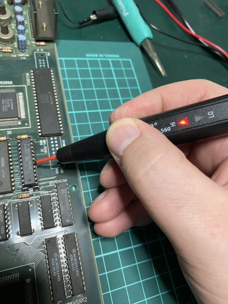
Let’s keep digging. At this stage of the repair, I take out my Logic Probe and start checking signals.
I see a High (No Pulse) signal on the 18th pin of the RAM. This is the Chip Enable pin. The datasheet shows a line over the label for this pin, showing that its Active Low. Thus, the RAM is not being enabled.
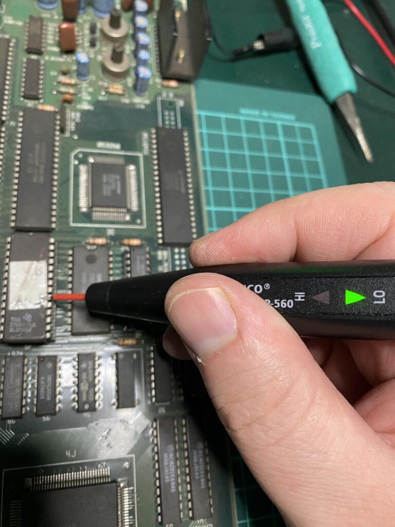
When I check the ROM, I see a LOW signal (No Pulse) on the Pin 20. This pin is also the Chip Enable pin for the ROM. Just like the RAM, the pin is labeled Active Low on the datasheet so the ROM is being enabled.
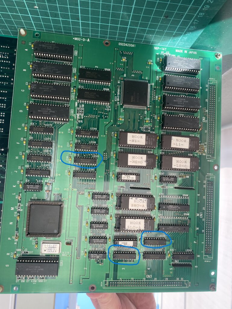
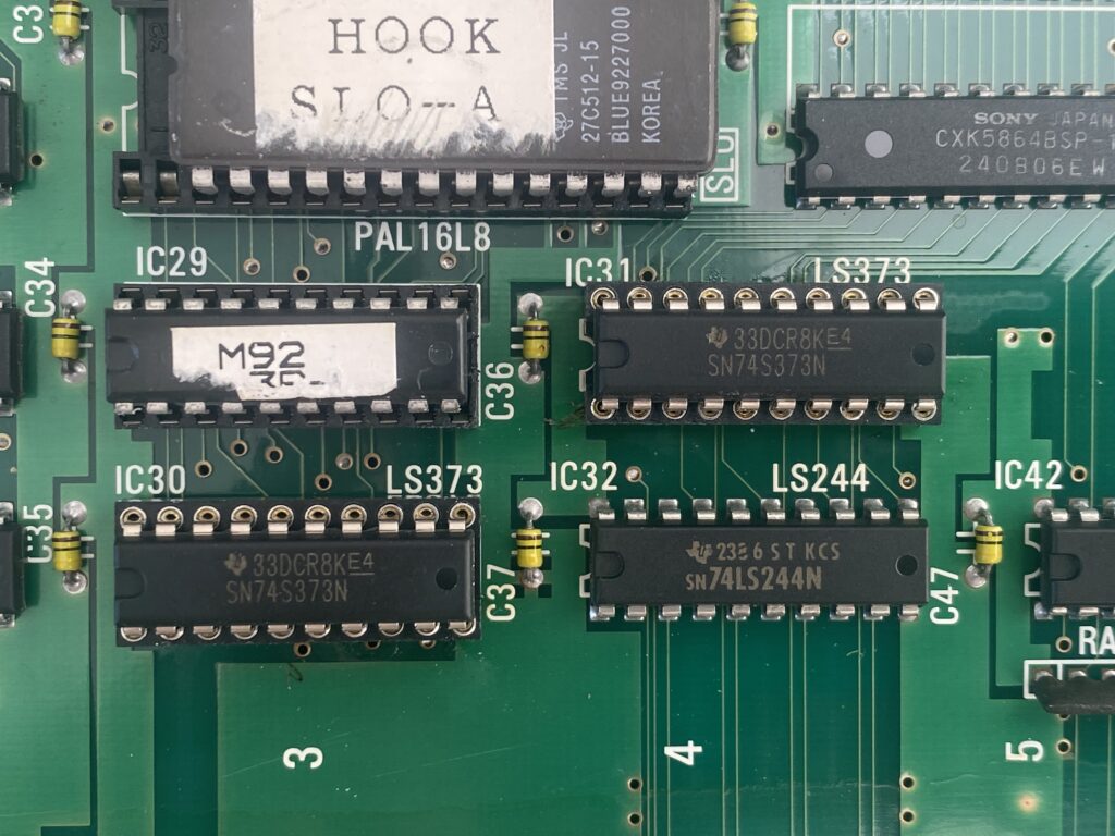
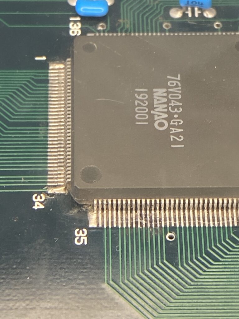
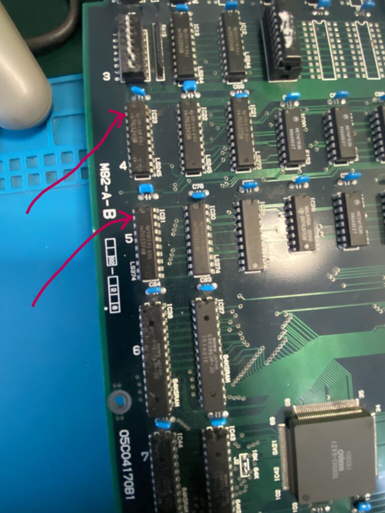
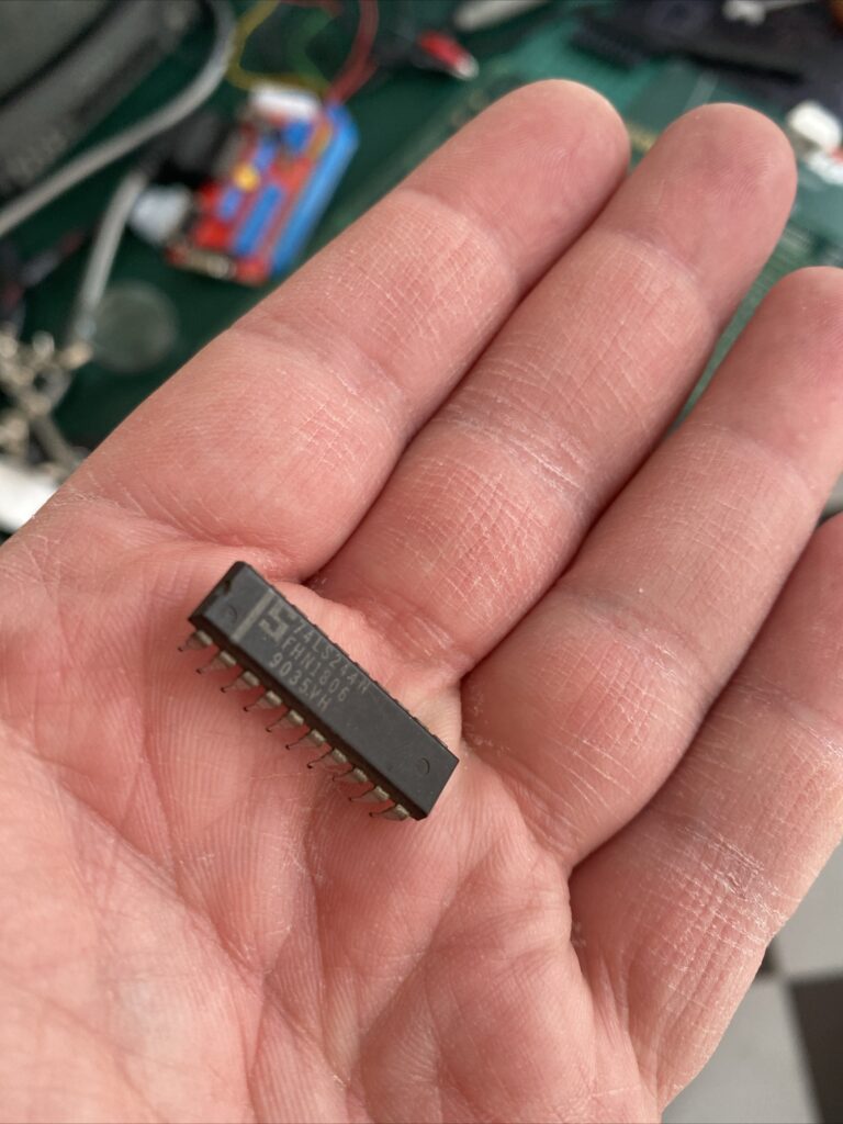
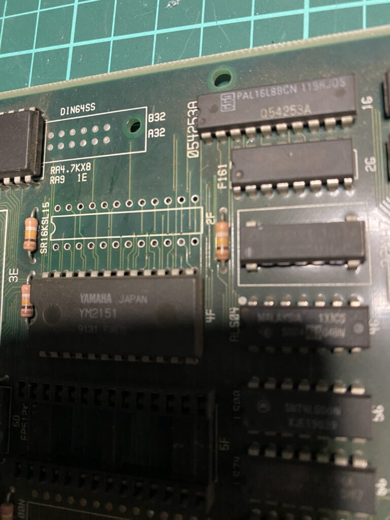
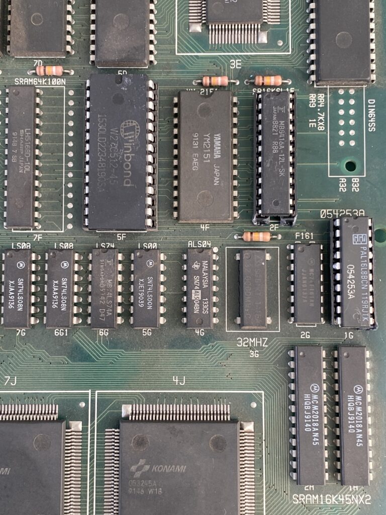
When I measure with a multimeter set to Continuity Test where the Chip Enable line of the RAM goes, I see that it goes to a PAL chip.
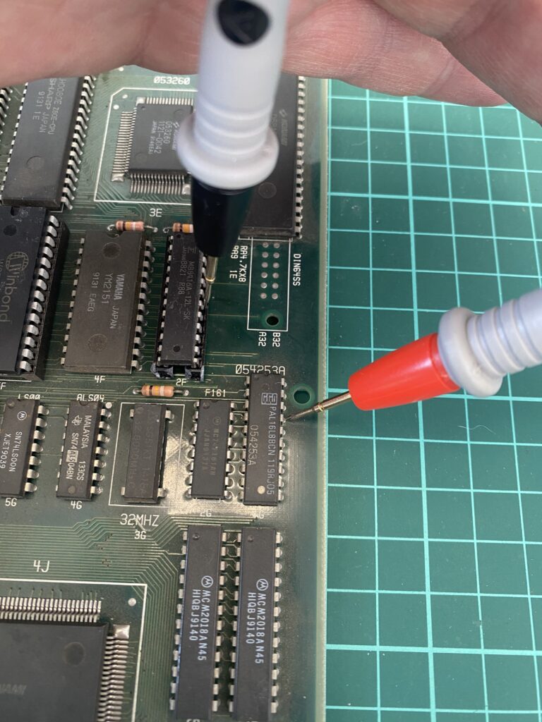
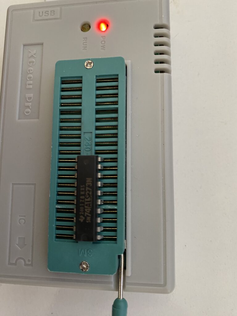
PALs are custom chips. If this PAL is faulty and has no dump, the only solution is to source a PAL from a donor board. If it has a dump (this one does), write the dump to a compatible GAL chip and use it.
[Editor Note: The PLD Archive website is an excellent source for PAL dumps.]
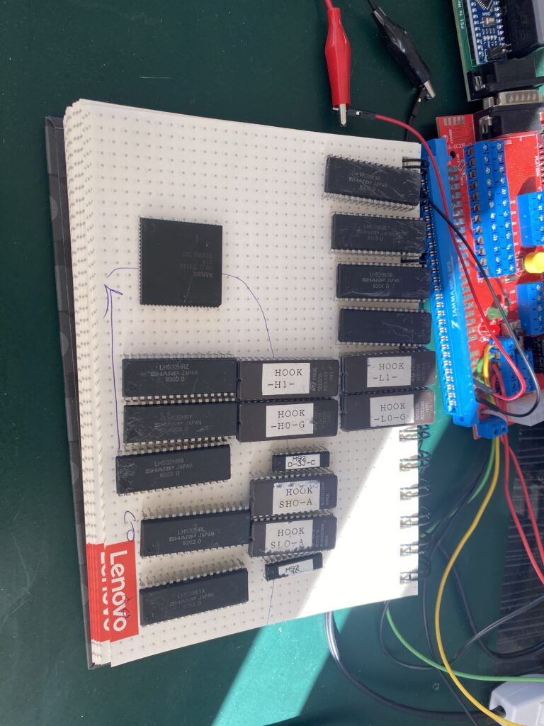
I don’t have a GAL but I have a better option – a working Asterix board! Having a working board to compare against is very useful when working on boards without schematics like Asterix.
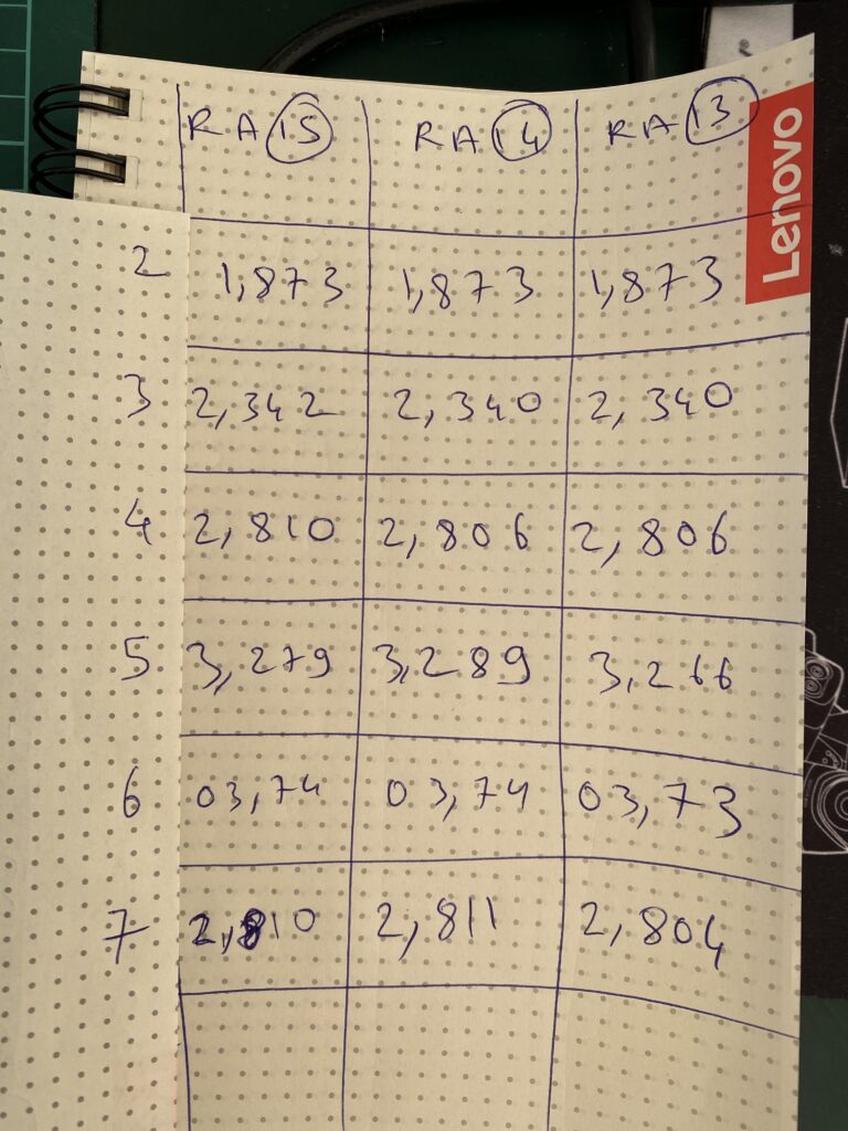
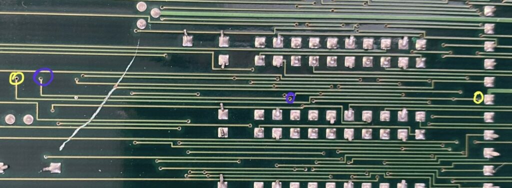
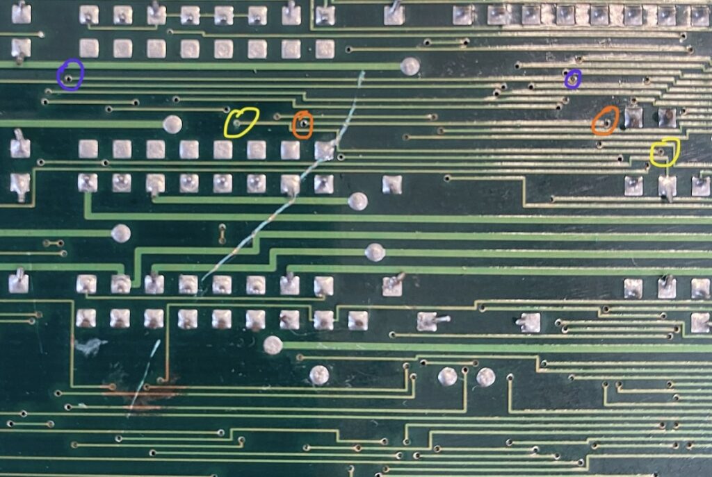
With the Logic Probe, I test the pins of the working and non-working board and compare the results. I do this test by powering each board off and on repeatedly through the startup diagnostic checks.
PAL TEST
H -> High
L -> Low
P -> Pulse
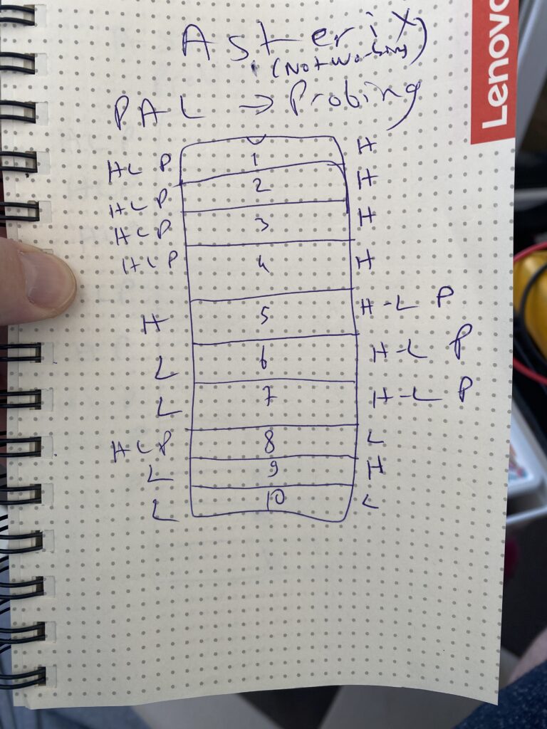
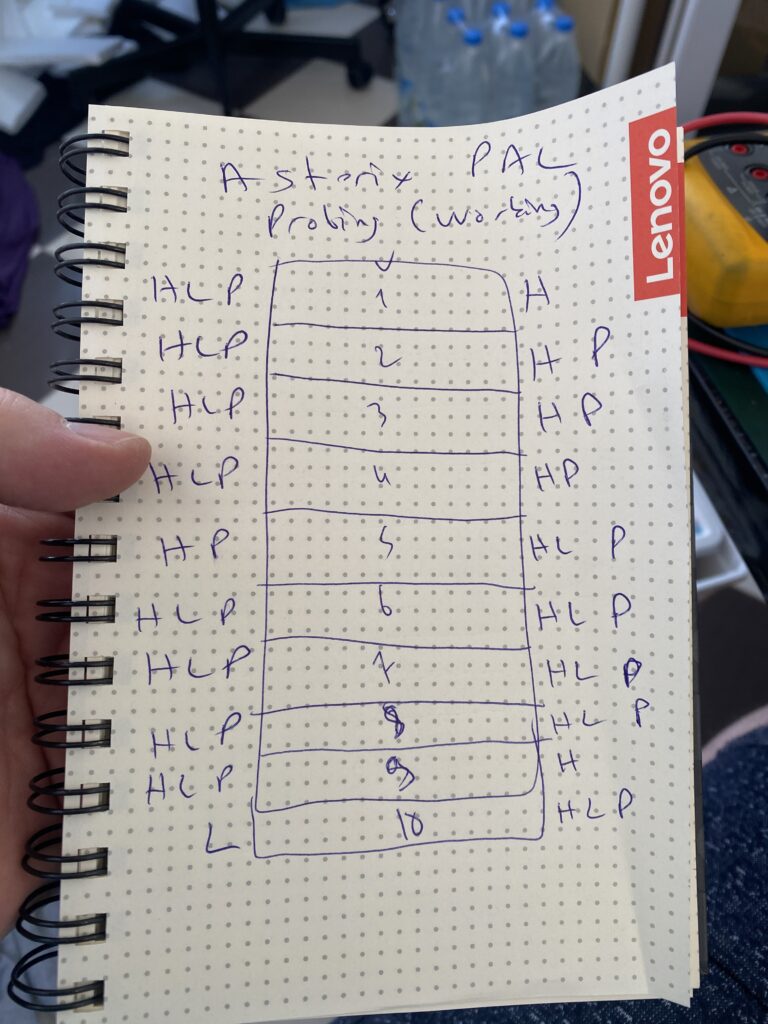
Quite different. There is no pulse on several lines on the non-functional board.
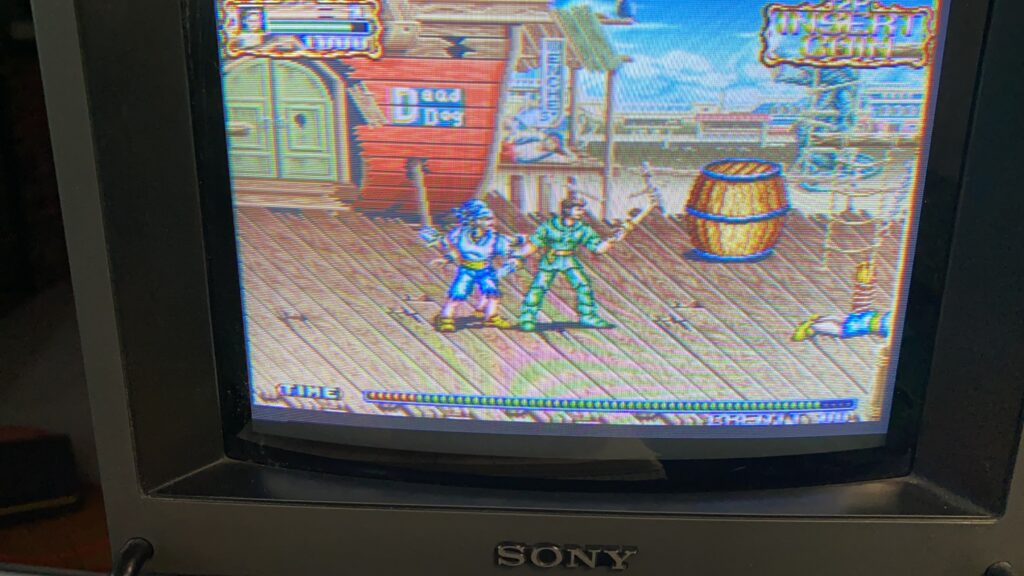
I’m confident that this PAL is the problem, and since I don’t have any GAL, I removed the PAL from the working board. You know the rule that if it works, don’t touch it? Arcade boards don’t have this rule 😀
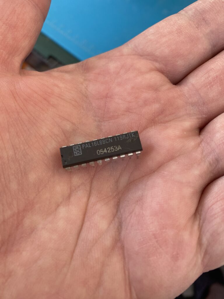
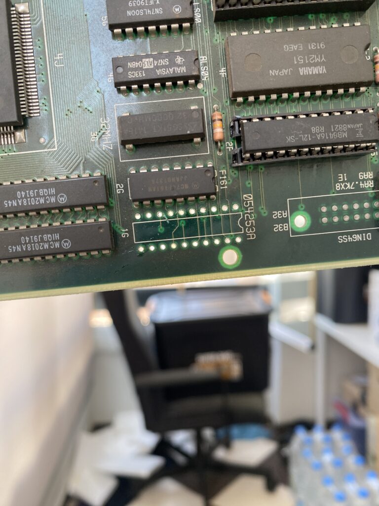
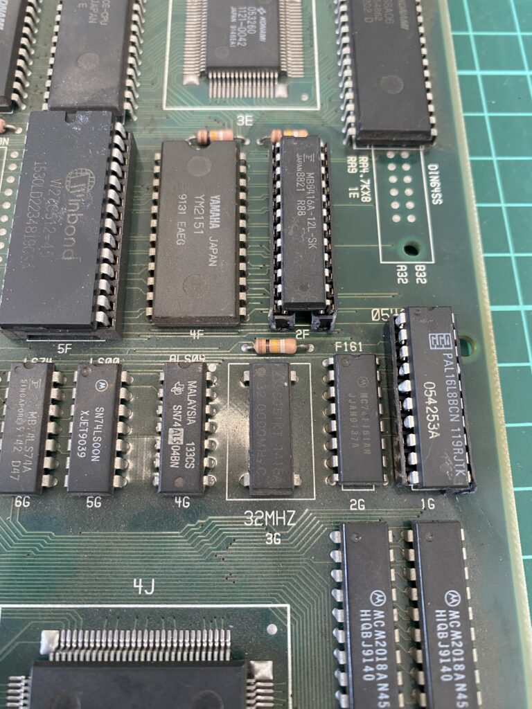
Here is the functional PAL, transferred from the working board to the non-worked board and socketed:
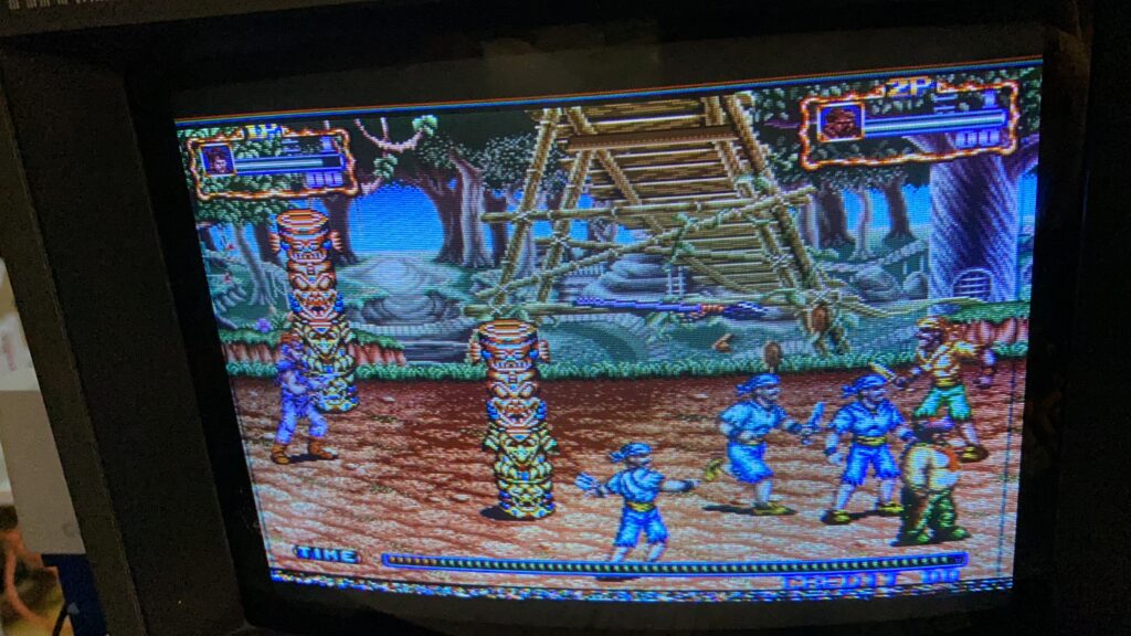
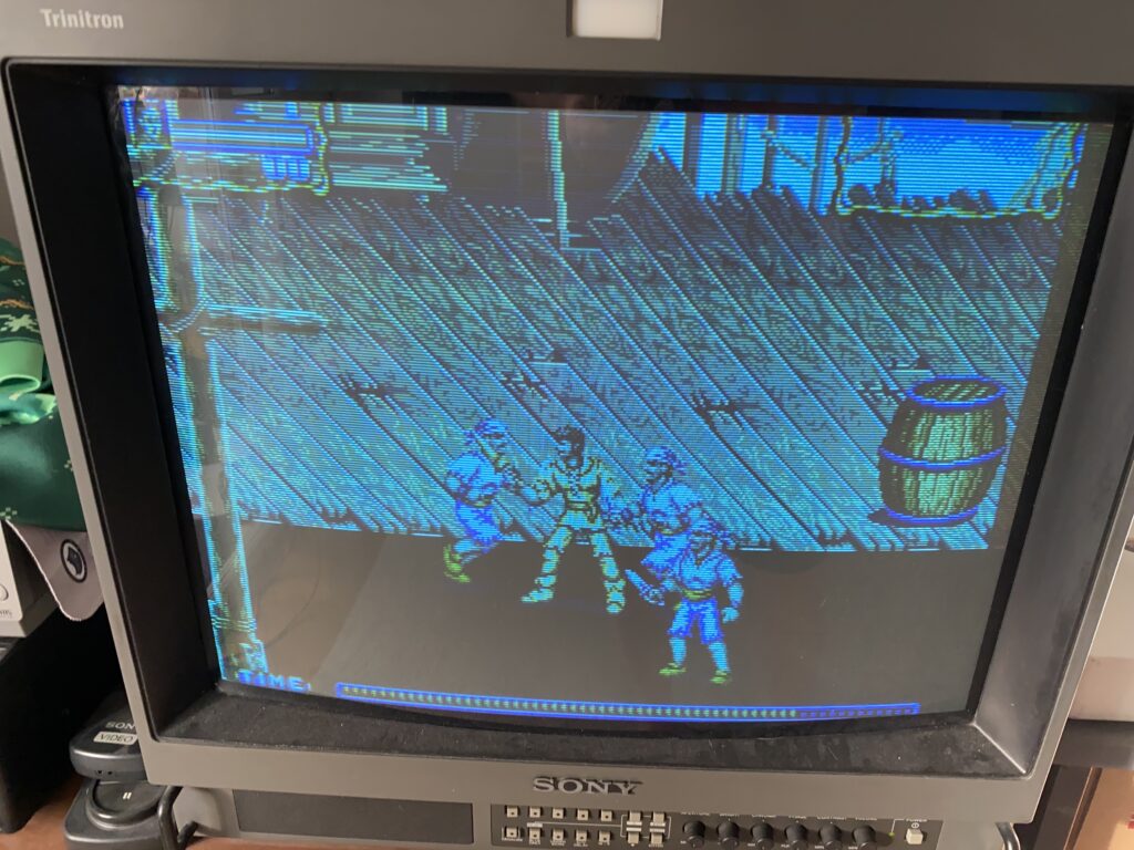
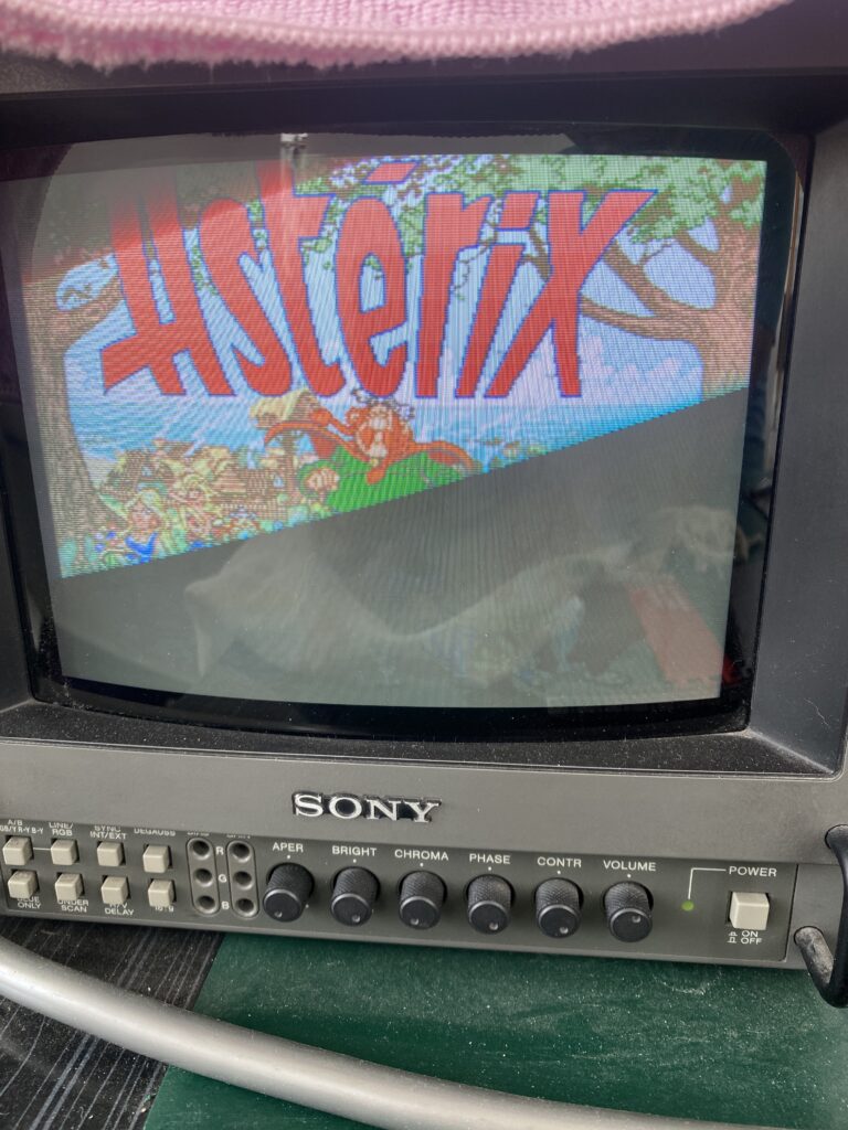
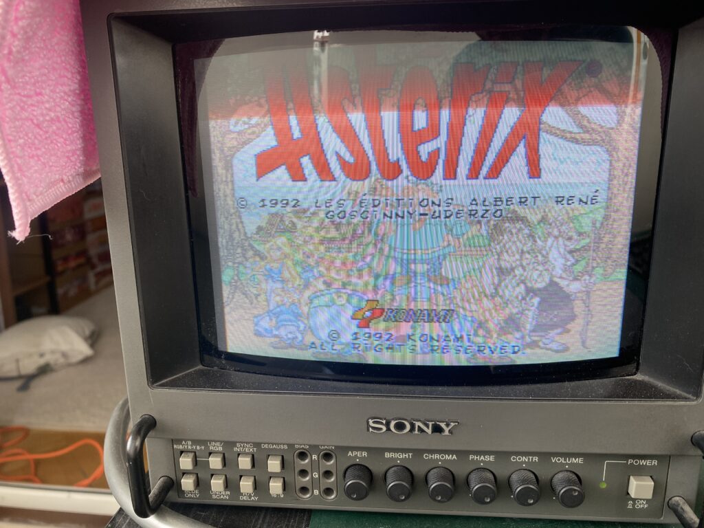
Time to power up!
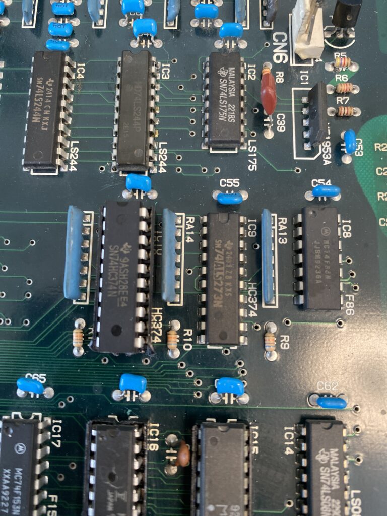
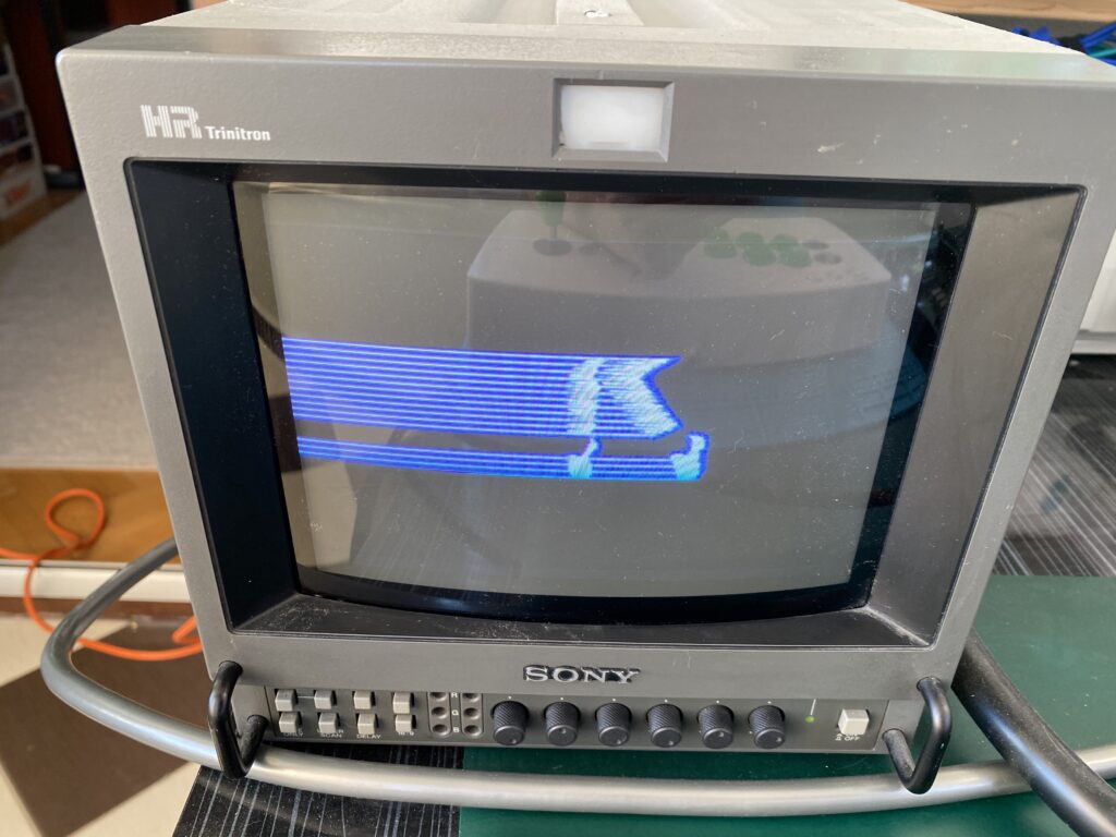
PFFFFFFFFF. Just when I’m about to give up, something catches my eye. Did you see it? Look a little closer..
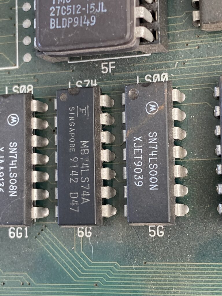
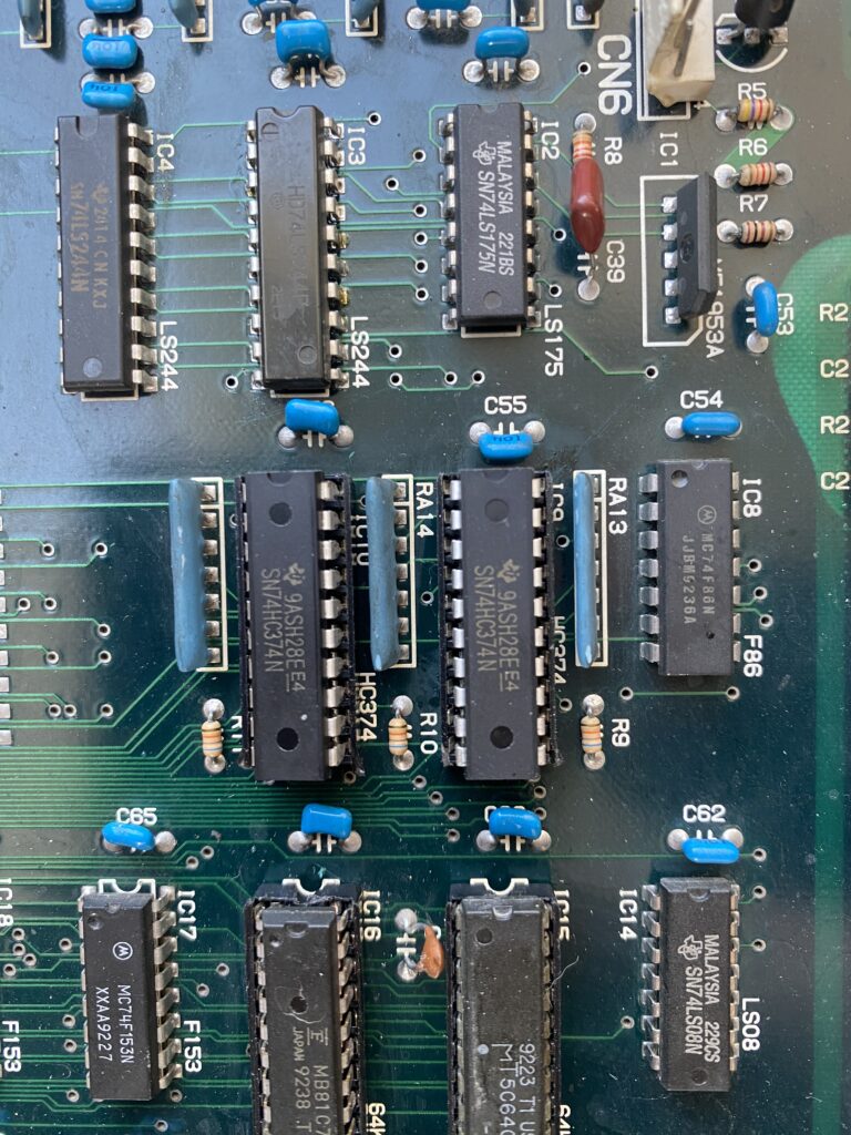
Yeah, right there… The IC with the F emblem. It’s a flip-flop circuit. But the important thing here is the brand. Fujitsu ICs are the most prone to failure. I take my Logic Probe in my hand and start probing from the top right pin on the chip (VCC). Let’s power up the board again…
Whoa! Before I can understand what the probe is saying, I hear horse footsteps…
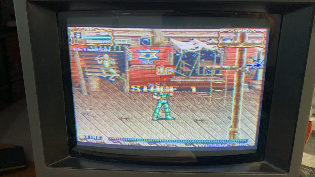
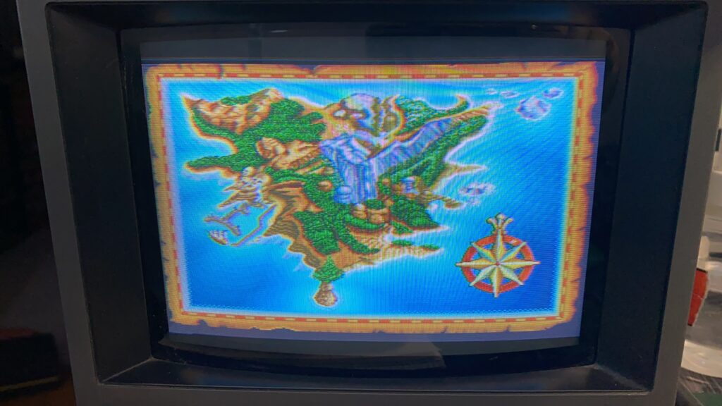
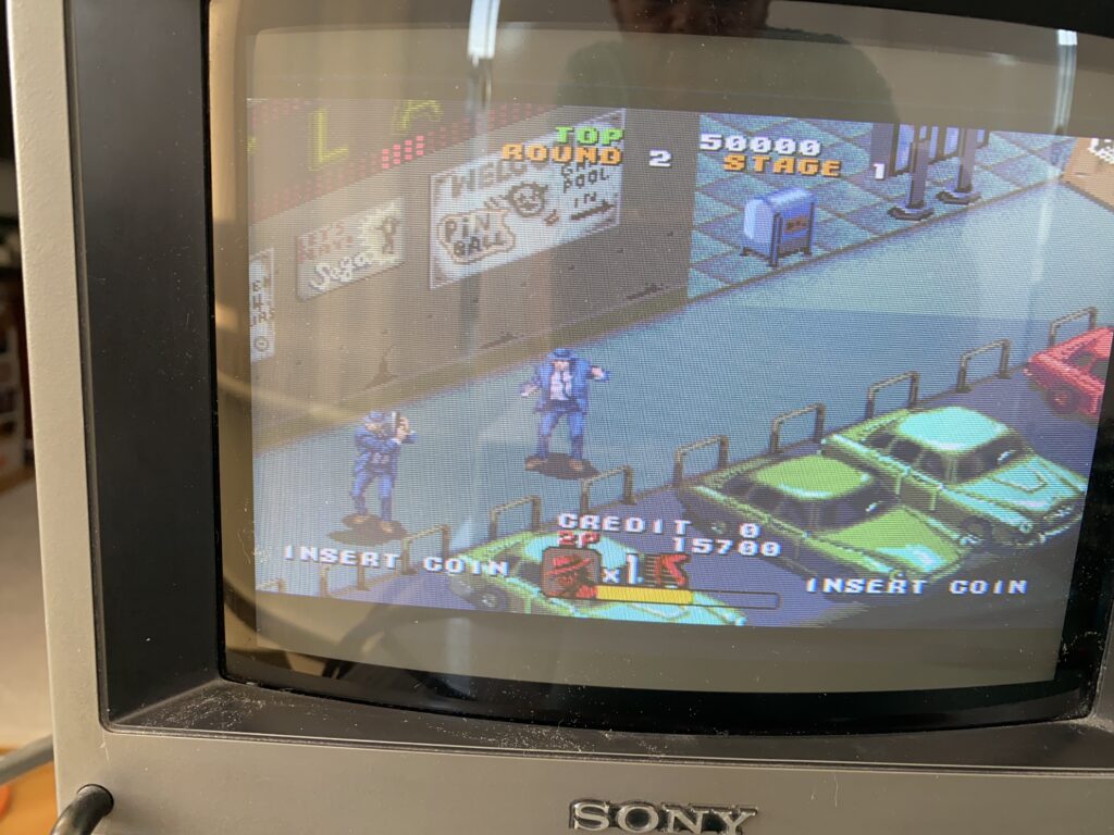
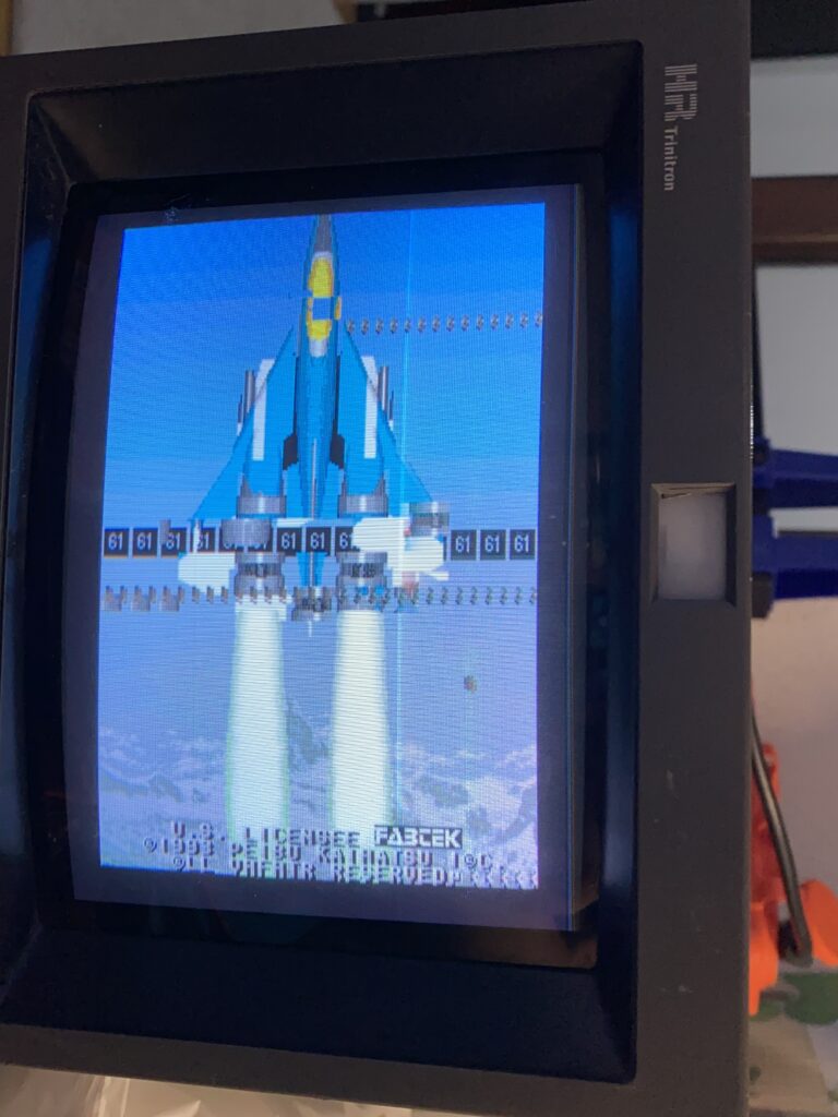
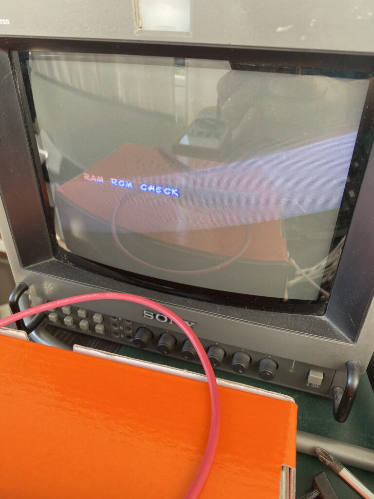
I don’t know what happened, but the board works now. I set the board aside for two days, and when I tried it again, it works fine. I have no idea if probing the VCC pin of that Fujitsu IC triggered something, but it works. I did not change out that part yet because it is working for now.
Best Regards
Oguz