Aug 272014
 

Game was dead on power up.
Pressing down on the crystal brought clocks back. Resoldering the crystal didn’t help so there must have been a break internal to the unit. I ordered a spare 18.432MHz crystal oscillator and waited for it to arrive.

The new crystal arrived and fitting it brought the main clock back however my monitor screamed at me.
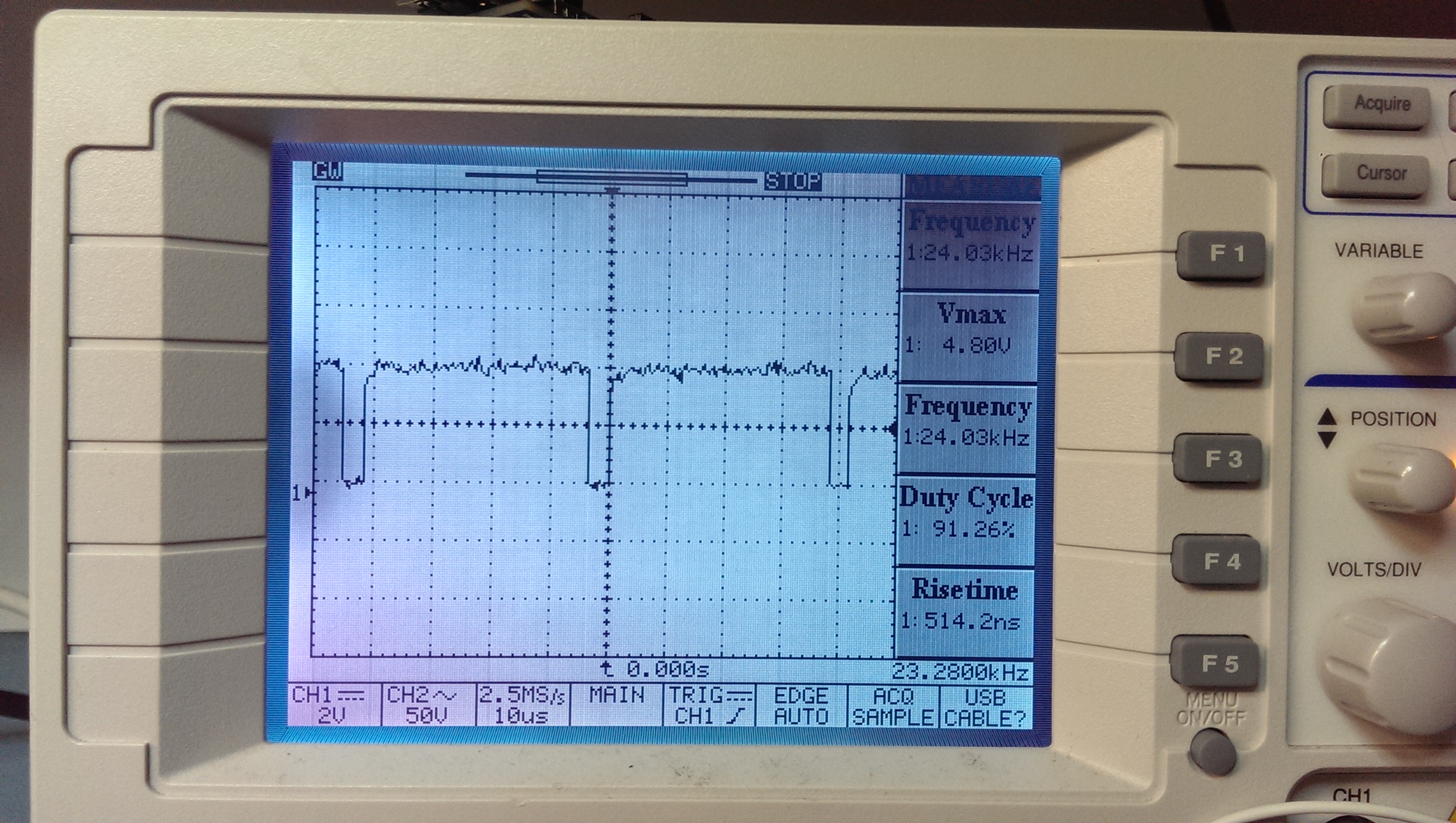
Checking the output from the 082 custom chip on the scope revealed that the SYNC signal was around 24kHz.
wrongkhz

I originally thought the 082 was at fault as id seen so many of them go wrong before but after sleeping on it I started to think this unlikely. At this point I asked for a bit of help from forum user cmonkey. He knows a lot about Konami hardware and has provided a lot of insight to me in the past.
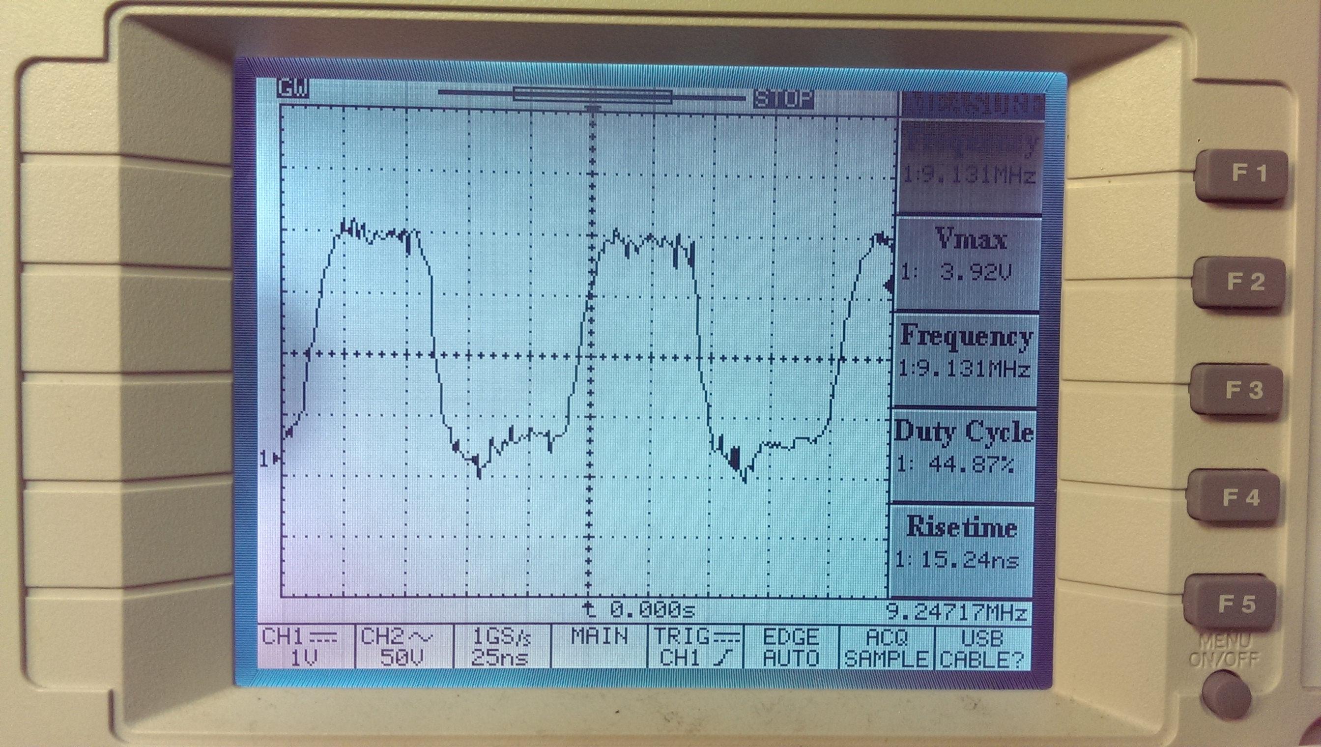
He very generously took some measurements off his Gyruss PCB and it confirmed that the clock input going to the 082 was too high on my board. It should be 6.14MHz into pin 13 and I was getting around 9.14MHz.
wrongkhz2

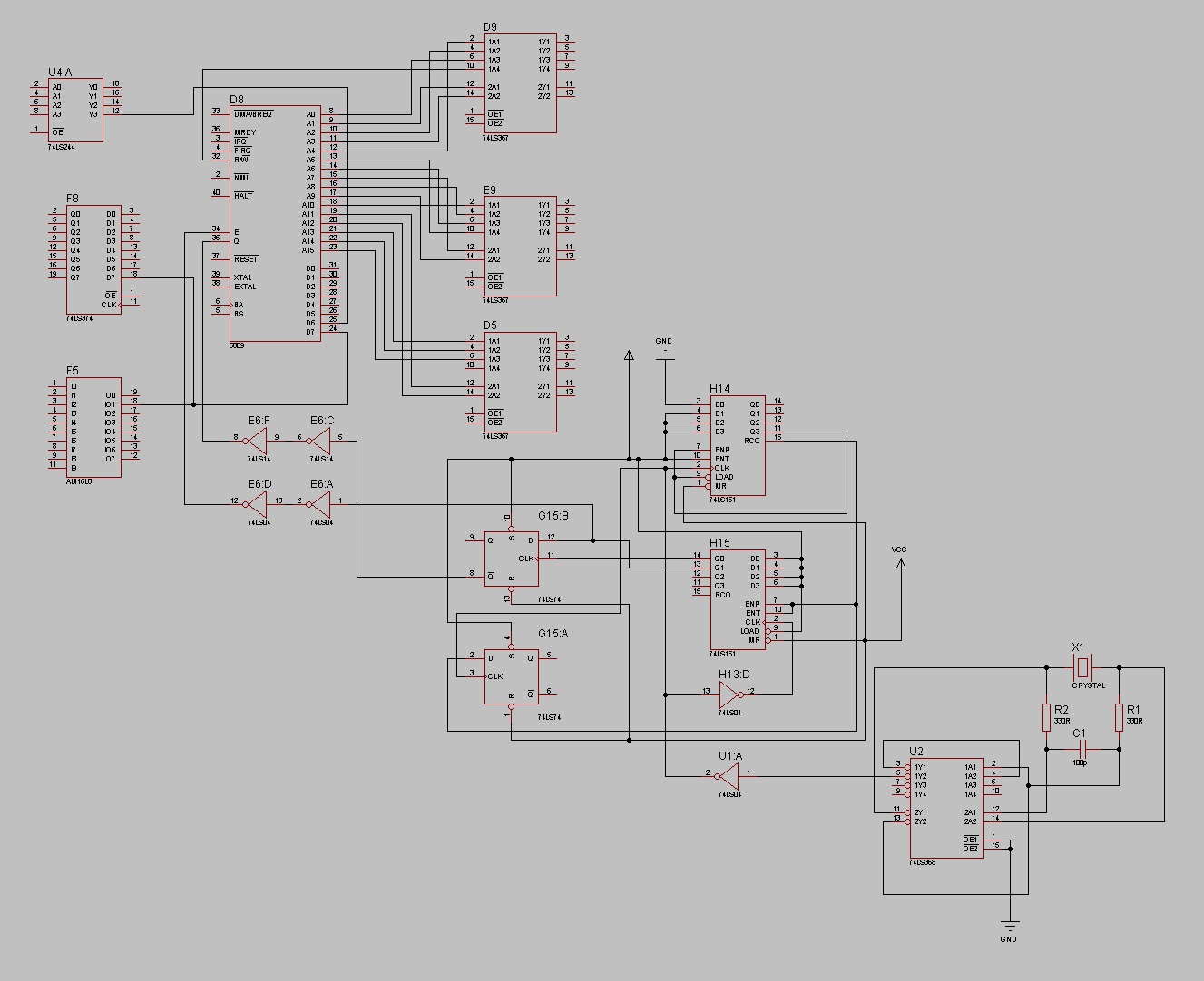
At this point I thought I would do a bit of circuit simulation and drew out the clock generation circuit in PSpice.
cc-sim1

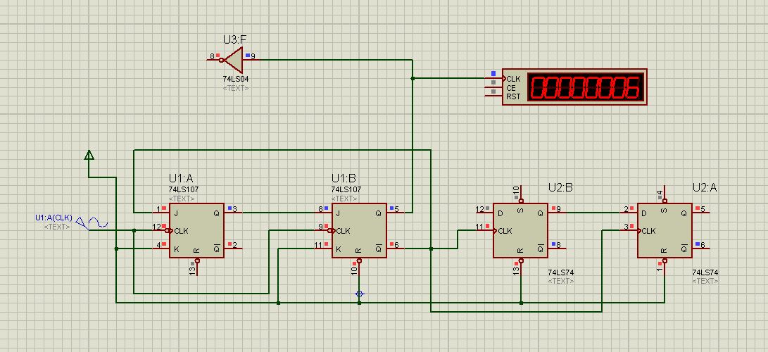
This is how the circuit should be.
ccharlie-clock

As you can see from the simulation I have around 6MHz.
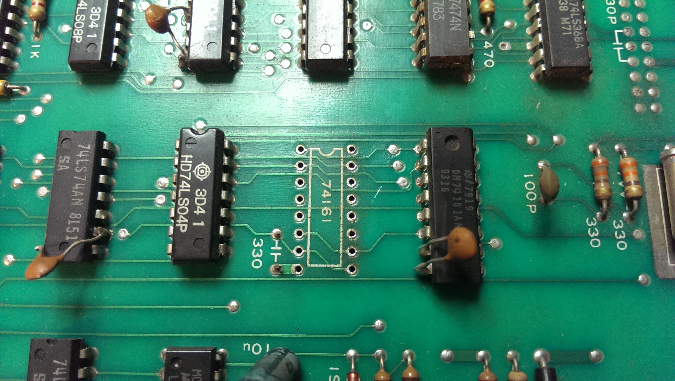
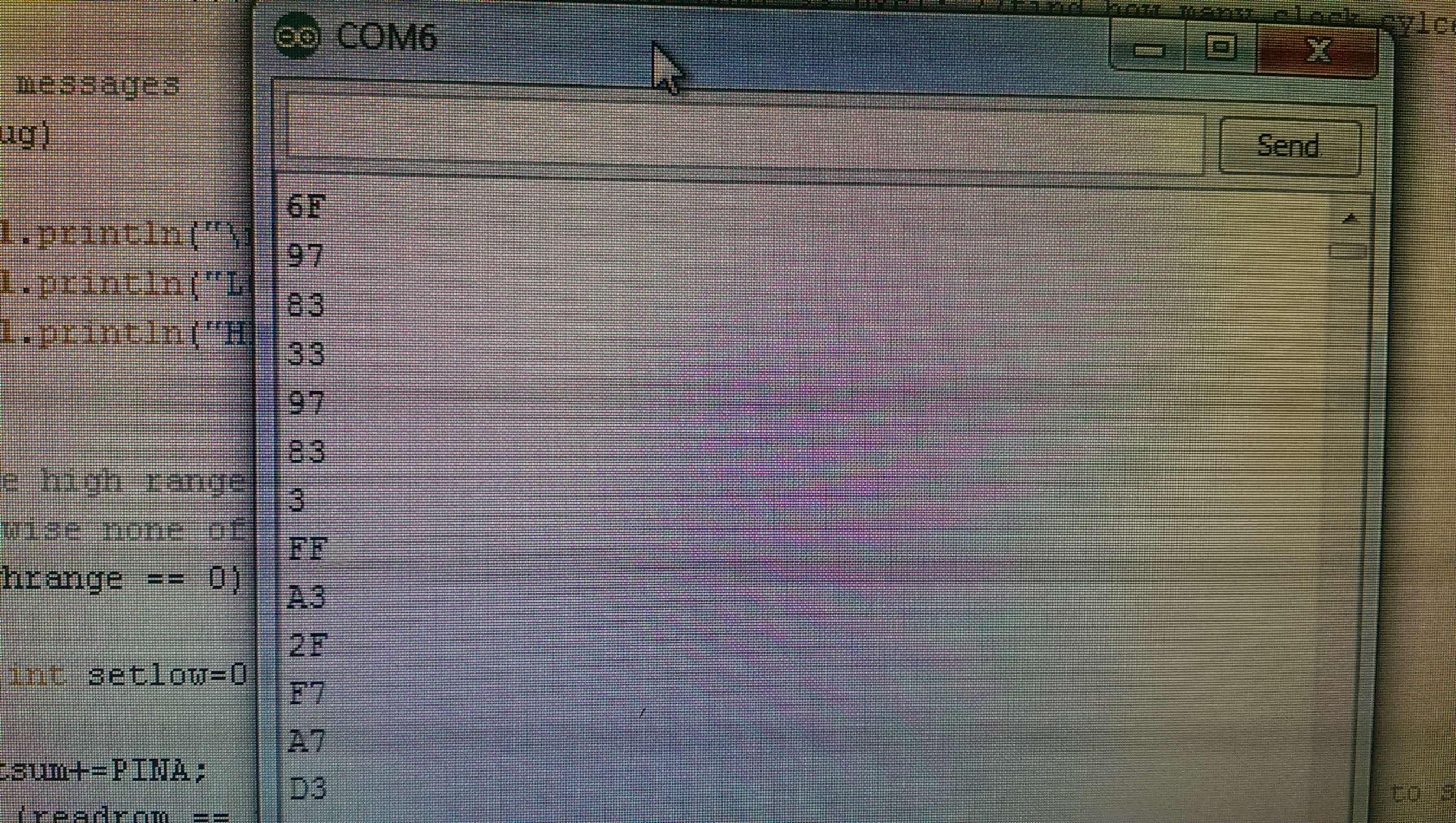
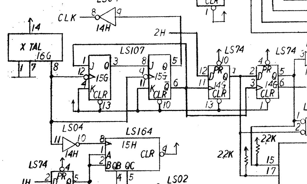
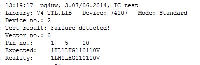
Probing around this PCB however revealed that pin 1 of the 74LS107 was dead. Removing this line from the simulation revealed this:
cc-sim2

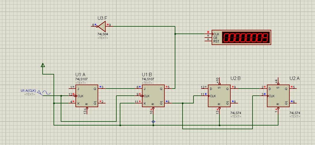
Exactly what I was wanting to see.
I removed the LS107 and tested it. It failed as expected.
cc-107fail

I found one on a scrap board. This brought everything back to life.
ls107

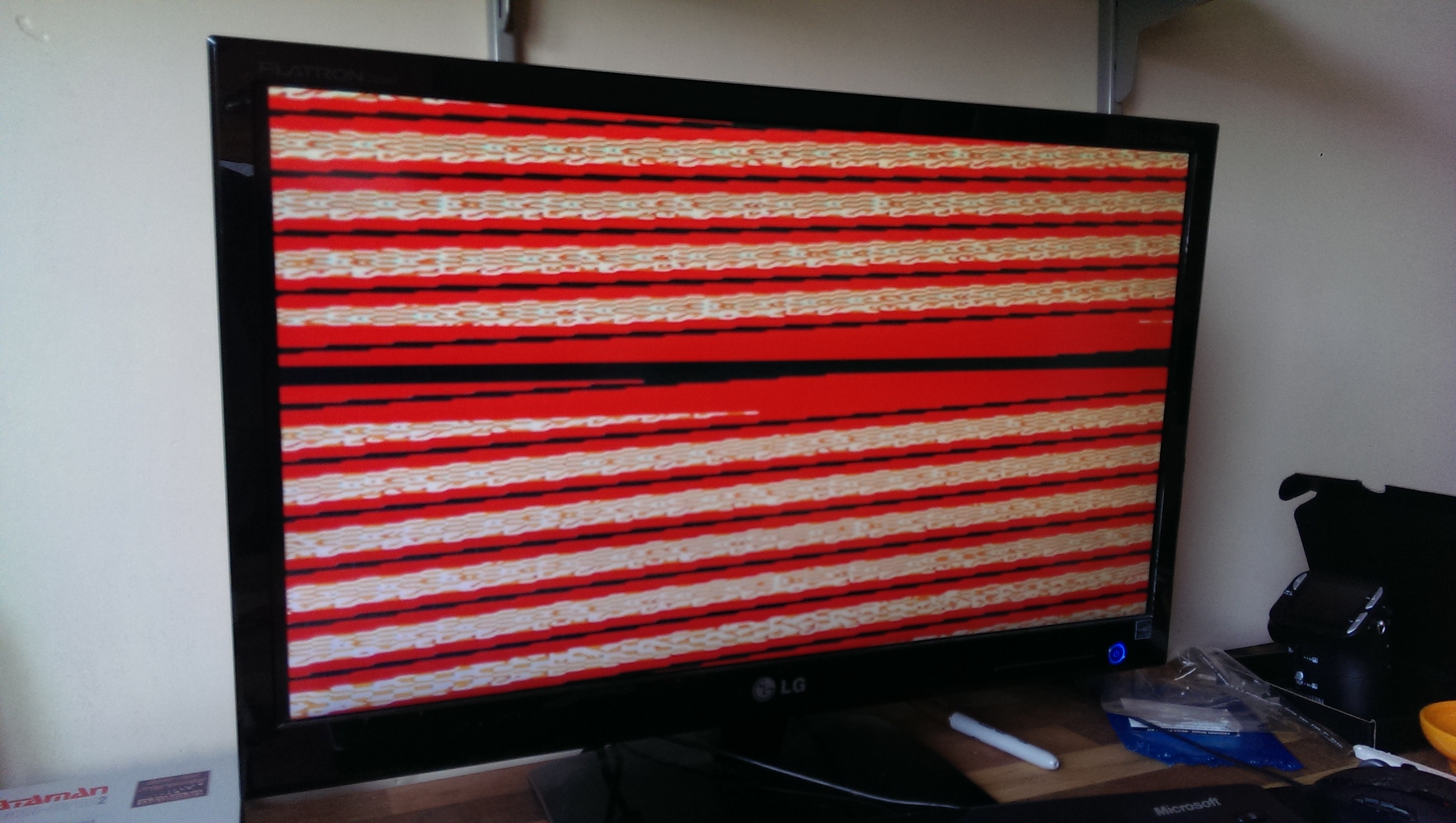
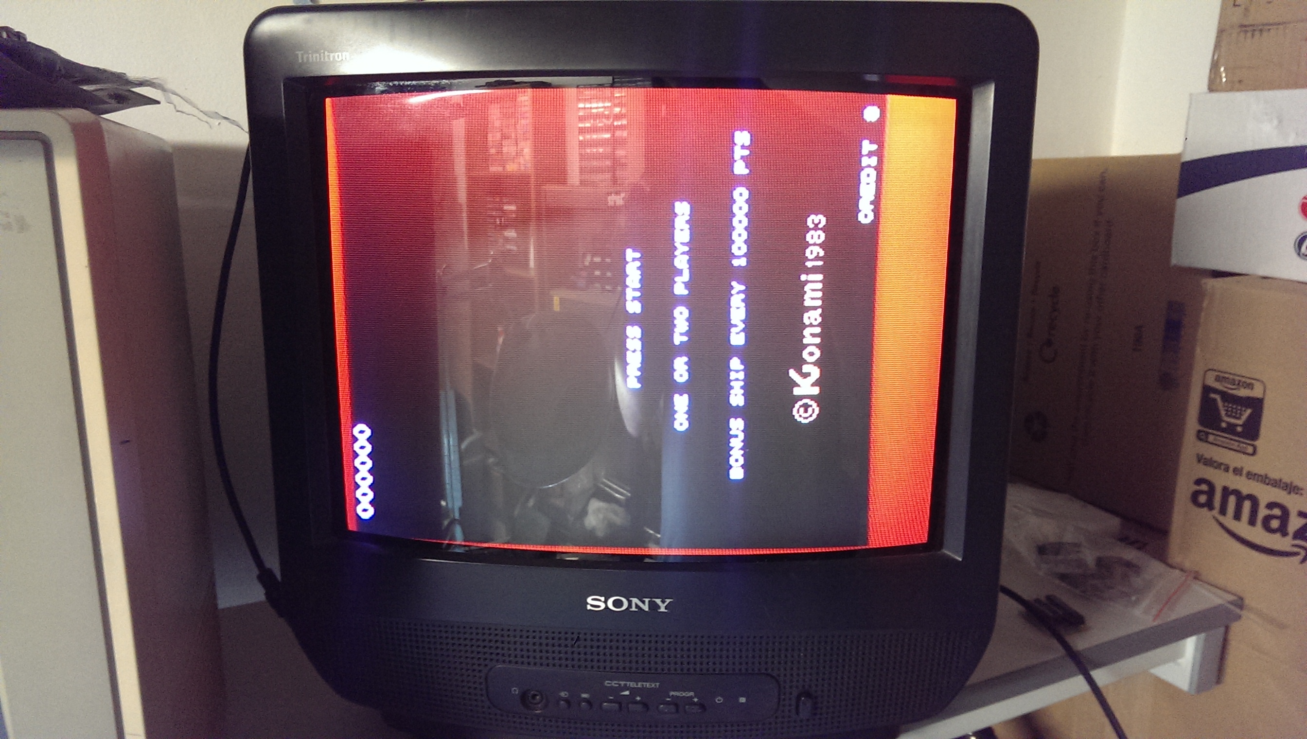
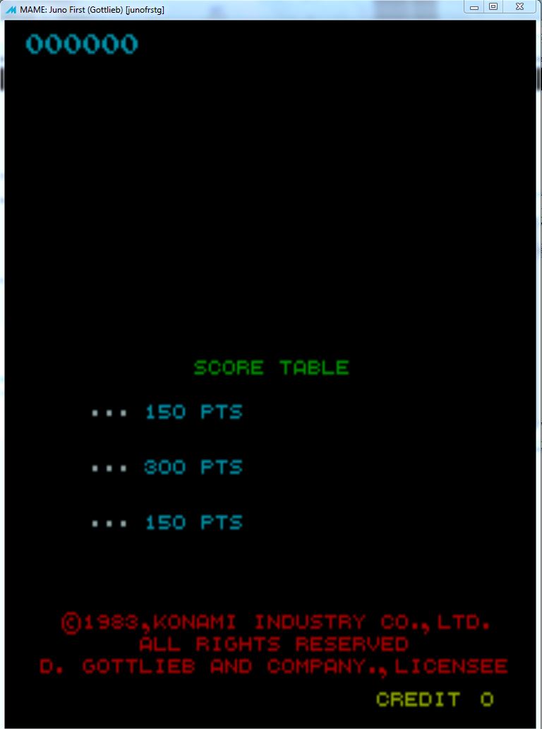
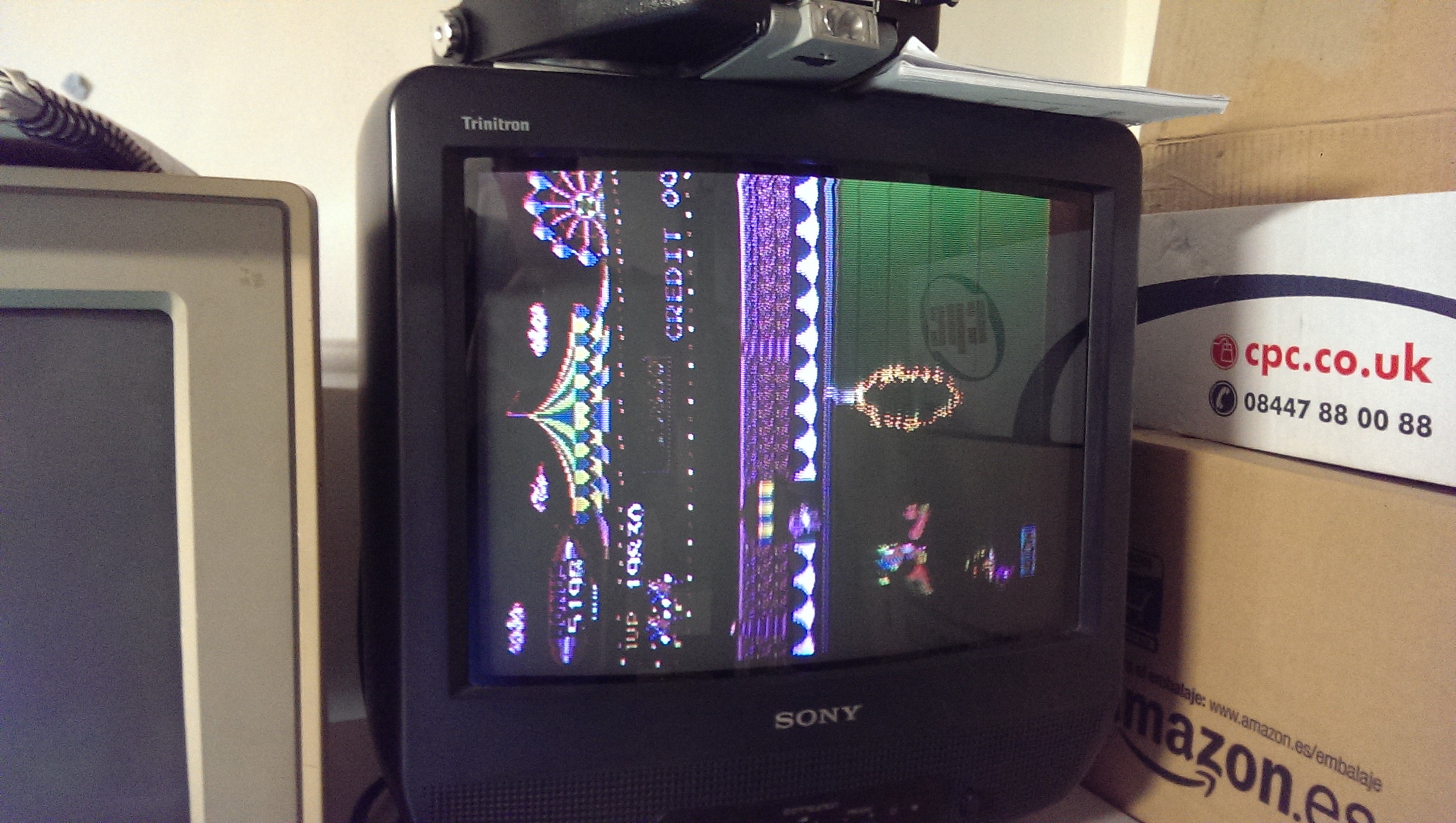
Powering the board up initially gave me a static screen of 0’s. This is what you normally see during the start of the POST. Ill get back to this issue later.
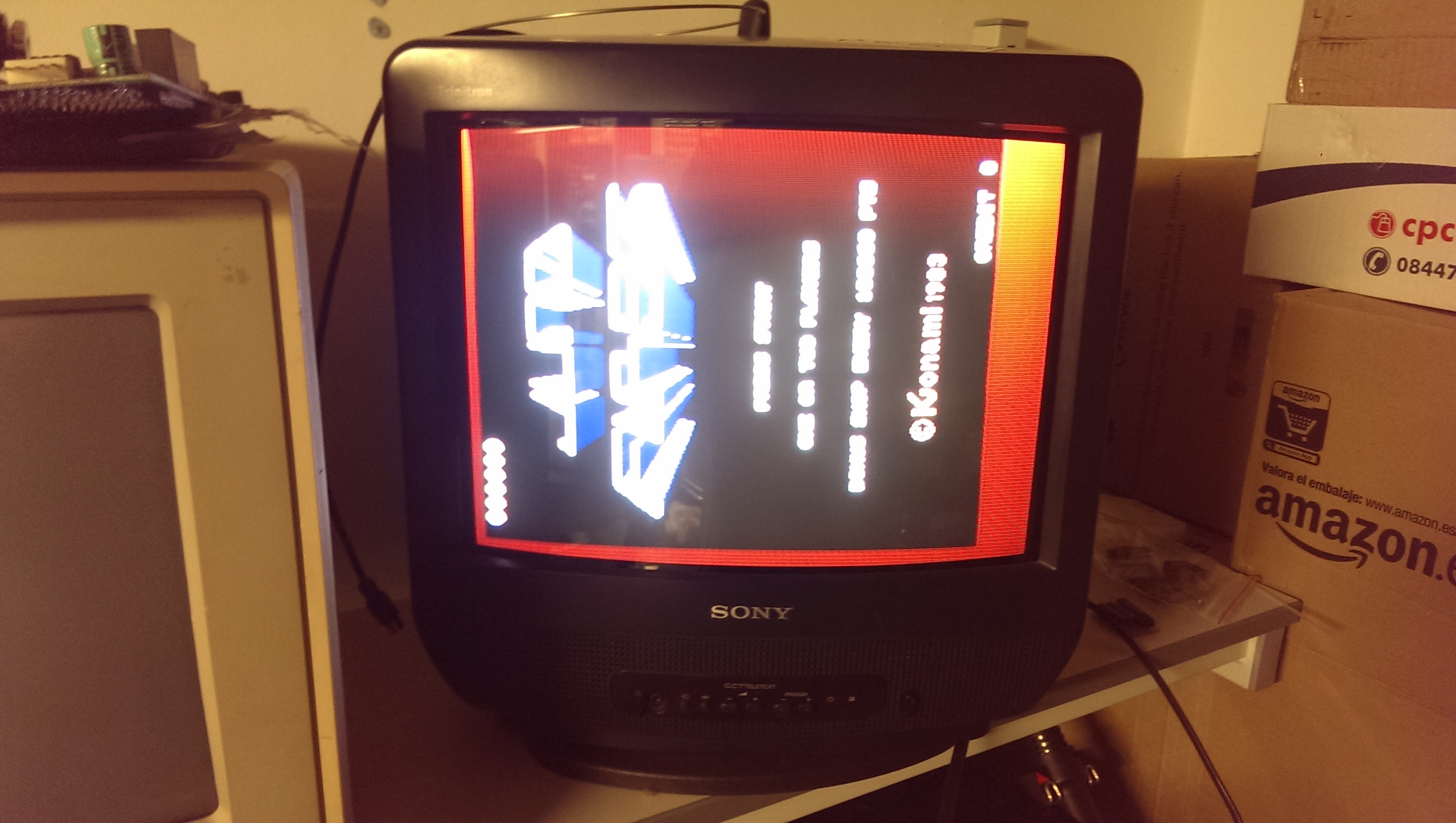
Powering down and back up again gave me this:
rightclock

Using MAME I confirmed the Video RAM area was to blame.
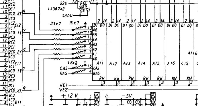
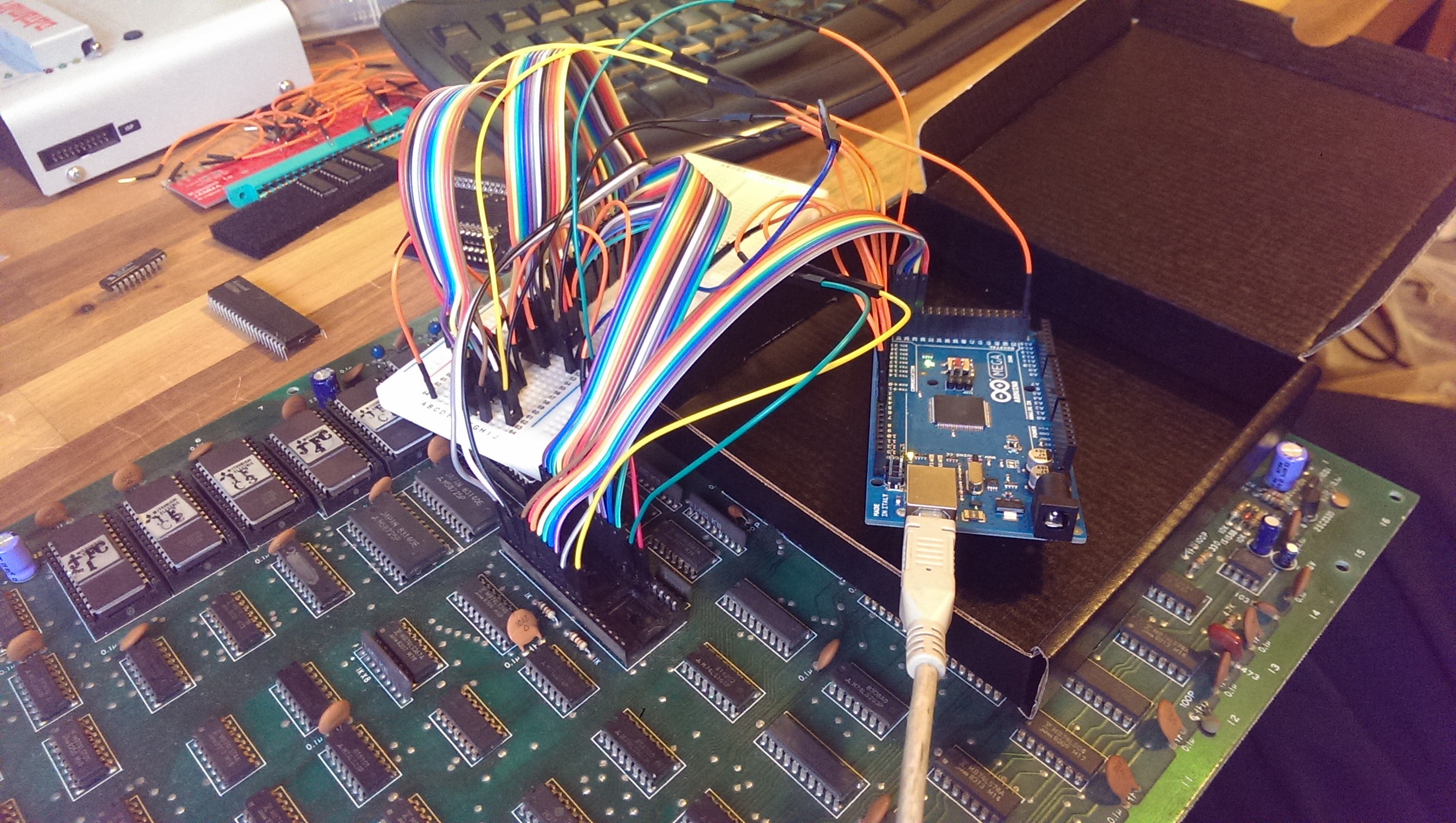
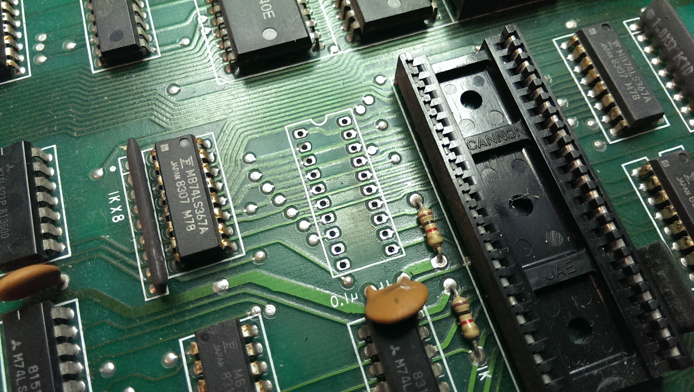
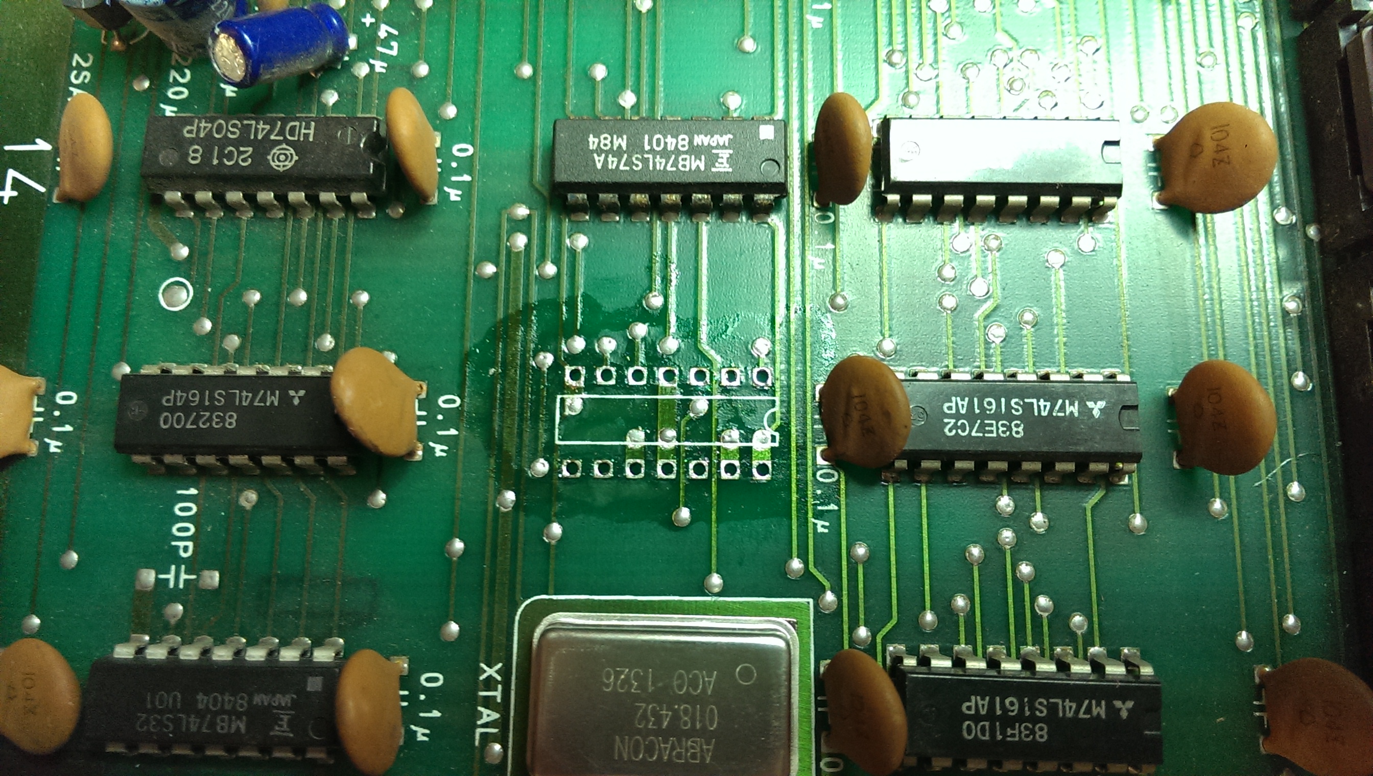
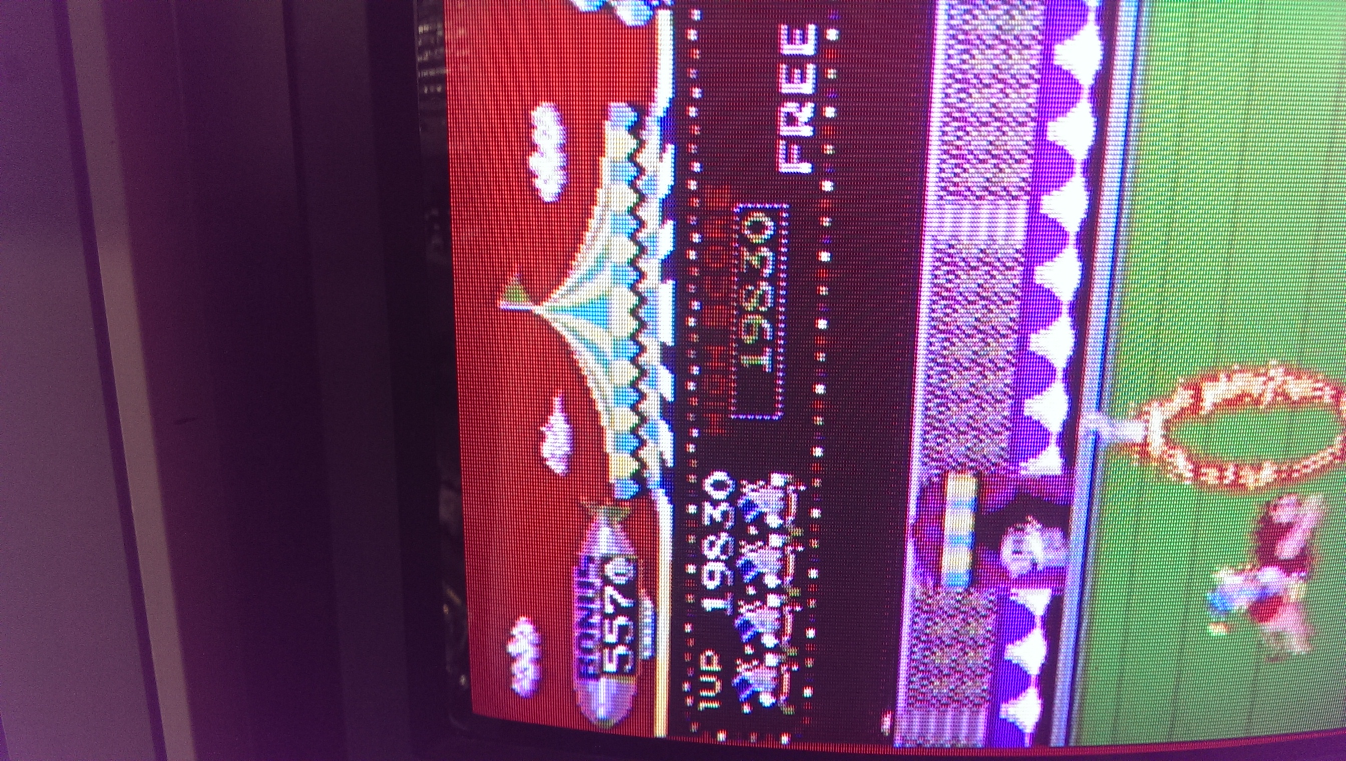
Checking the address lines on the 8128 RAM at location 3E revealed 4 dead lines. I traced these back to 74LS157 at location 5E. Replacing this brought back the graphics.
almost

There is still a small graphics issue at this point which I struggled to find and also the intermittent power up problem I mentioned earlier so thought I would move on to the other issue of the controls not working.

Neither of the coin inputs work.
Back to the schematics, I can see where the signal comes in and taking some measurements shows there is something wrong as I’m getting around 1v at pin 6 of the chip at 3F.
There is very little to this part of the circuit and the resistor array looked good so I desoldered the 74LS253 and it failed all tests. Replacing this brought the controls back.

So back to my remaining problems.
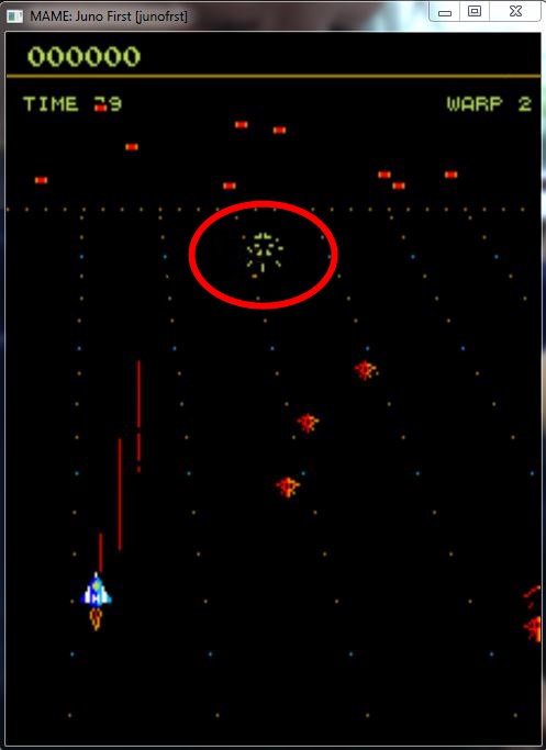
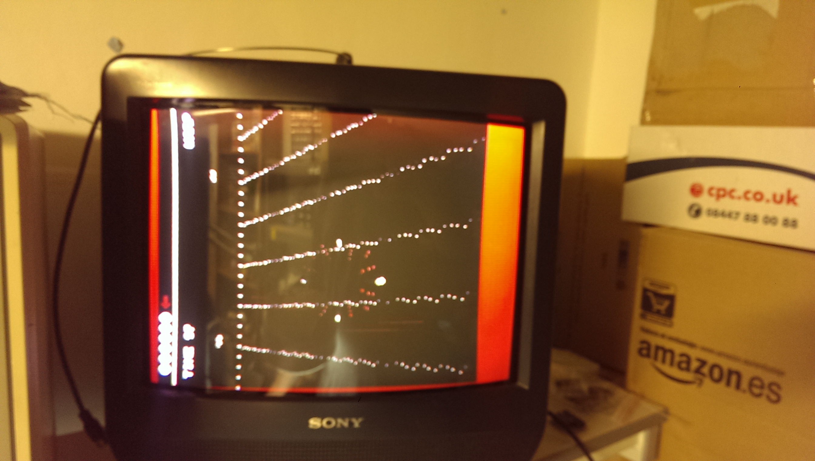
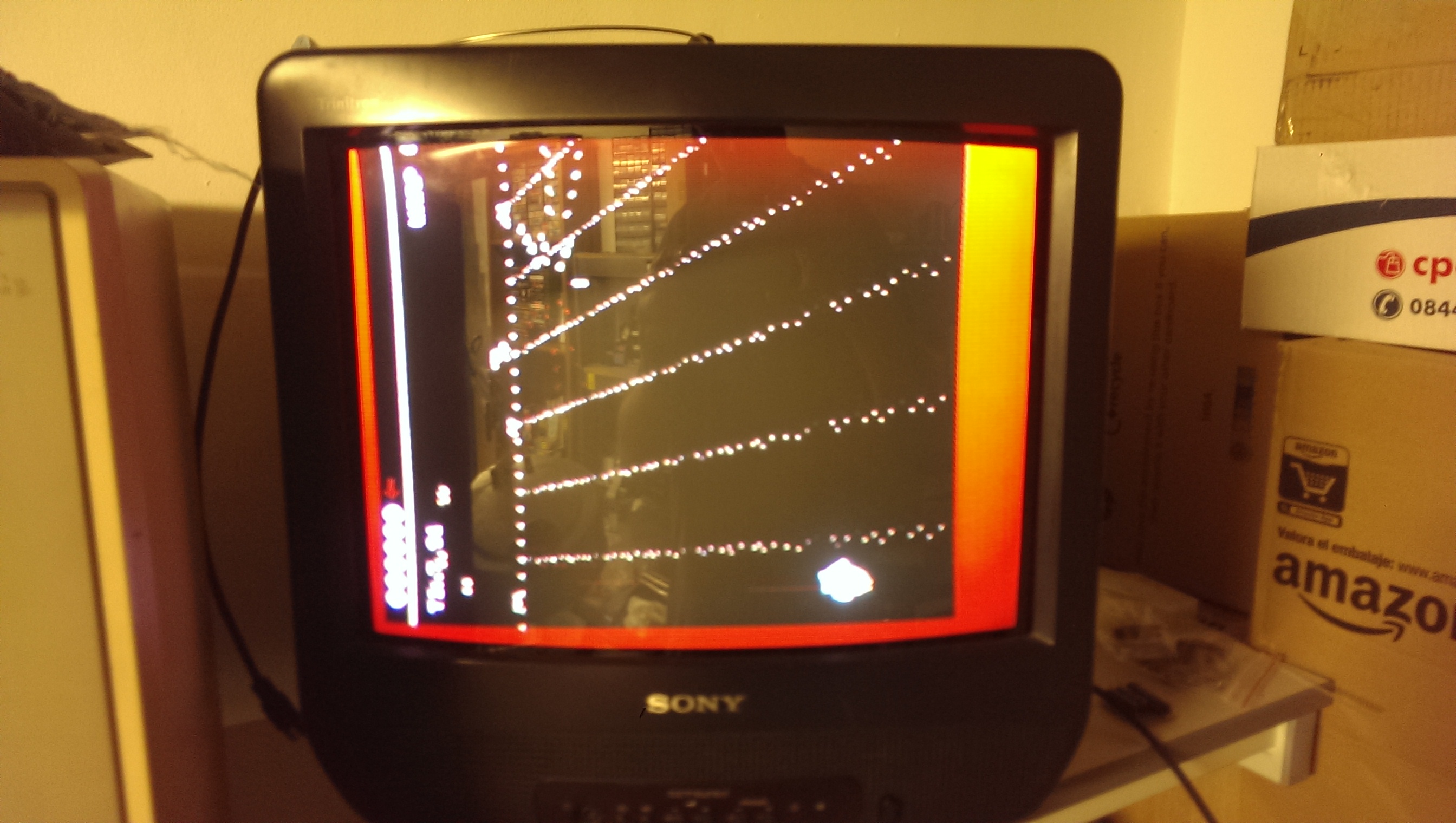
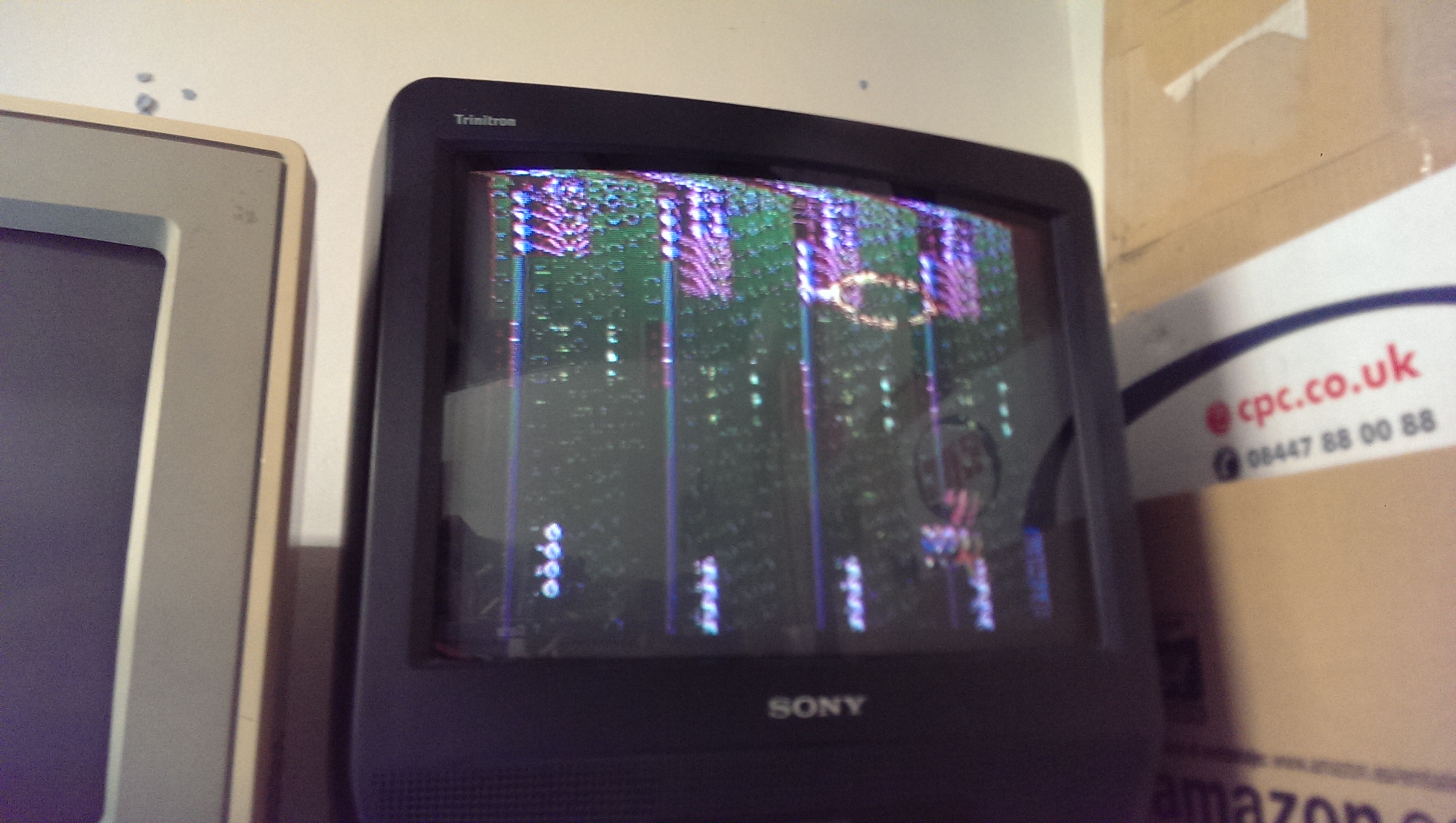
First, the graphics issue. Its hard to describe but on the parts of the screen where the coloured dots cycle round this also affected half of the 8×8 tile above it.
IMAG0820

As it only affected half the tile I eventually came to the conclusion it was a timing issue. This led me right back to the beginning where the reset circuit lies.
The power on reset is generated by a 555 timer which goes through a bit of logic and eventually out to the rest of the board as a /RES signal.
cc-reset

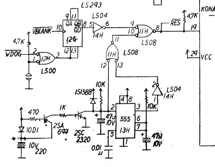
This signal comes out on pin 8 of a 74LS08 AND gate. Working back I found I had no output on pin 11 at all. I desoldered this chip and replaced it.
IMAG0816

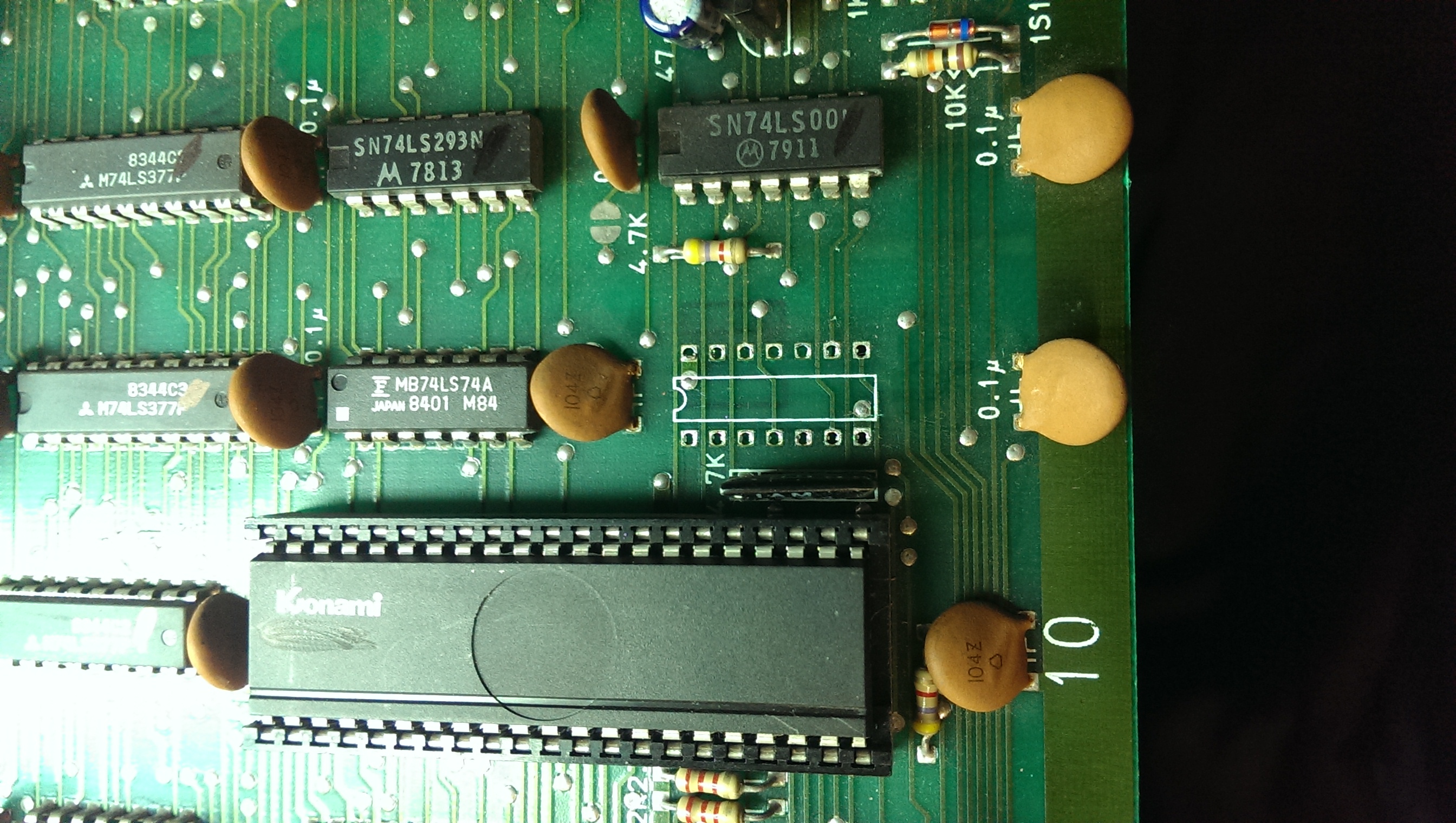
It fixed the reset problem but also fixed the graphics problems too
IMAG0821

I guess it could have been caused by a timing issue after all?

This board looked is VERY good condition and, looking at the edge connector, it cant have been powered up more than a handful of times so its interesting to see that all these problems were present.
Very pleased I got this fixed.

Juno First repair log #3

 PCB Repair Logs, Repair Logs  Comments Off on Juno First repair log #3
Jun 262014
 

Third repair log from the batch of Juno First boards.
On power up the board was completely dead. No clocks were present on the CPU or many other IC’s.
As this is a bootleg board the available schematics do not fully apply and the clock circuit is normally handled by custom chips so this was a bit of a learning experience.
To help in dealing with this problem I started making my own schematics up.
junobl

Using a logic probe I could see that the outputs of the 74LS161 @ H14 were all HIGH. As there is no clock present to this chip it should not have counted anything at this point and they should all be LOW. This meant to the board was booting up in an incorrect state and the clock circuit was never starting.
I desoldered and replaced the offending 161 chip.
IMAG0616

The clocks were now all present but I just got a static blue screen and the watchdog was constantly resetting the system.
Using my in circuit Arduino tester I knew the ROMs could all be read correctly by the CPU. I also knew all the program RAMs were fine.
Replacing the 6809 CPU allowed the game to boot properly.

Next problem was the sound or lack of it.
The sound CPU is a good old Z80 so I fitted the Fluke and did a ROM check. This reported back an incorrect signature and when I removed the ROM I see this
IMAG0618

The VCC pin was missing. I soldered a new pin onto this and this board is fully fixed.

The last bootleg board has been a major pain and at this point in time I have admitted defeat with it. I have also been harvesting parts from it to fix the others so it will be written off.

Juno First repair log #2

 PCB Repair Logs, Repair Logs  Comments Off on Juno First repair log #2
Jun 152014
 

So here is the second repair log.
Pretty simple this one but I never took any pictures of the actual fault so Ive taken a snapshot of the event in MAME to show it.

The game plays as normal but when the blue ball enemies spawn into the game the froze up on screen and did nothing as circled in red in the picture below.
juno2

On my visual inspection I noticed a 1K pull up resistor array next to the bank of 4116 RAM chips what cracked in half.
juno2-1

Replacing this fixed the fault.

I did initially think there was another fault as the ship movement in attract mode seemed a bit strange but after checking in MAME this is a characteristic of the non Gottlieb version. In the Gottlieb version this behavior is not present.

Konami 007644 custom chip

 General, Technical Info  Comments Off on Konami 007644 custom chip
Jun 132014
 

Ive got a board that needs a new 007644 custom chip.
While im waiting to find a new one I thought I would investigate how this chip actually works.

Pin 1 = SEL – changes whether the Q outputs require a rising edge clock or not.
Pin 2 = OEY – Output enable for the Y outputs else they are inputs. Active LOW
Pin 21 = OEQ – Output enable for the Q (clocked) outputs else they are inputs. Active LOW
Pin 12 = CLK – Clock input

Pins 3-10 = Y outputs – normal outputs. If OEY is LOW these pins become outputs mirroring the state of the Q input pins. SEL and CLK pins are not used in this mode.

Pins 13-20 = Q outputs – clocked outputs. If OEQ is LOW these pins become outputs. If SEL is HIGH and CLK is HIGH these outputs will mirror the state of the Y inputs. If SEL is LOW then the outputs will only change state on a rising edge CLK.

Pretty simple and should be easy to implement in a small CPLD if ever required (next project???)

Jun 062014
 

This is hopefully one of five Juno First repair logs.
Thanks (I think) to muddymusic I have a stack of these needing repaired. There are two originals and three bootlegs altogether and decided to make a start on the originals first.

This one booted to an unsynced red picture.

Looking at the schematics I could see that the sync is generated by custom chip 082 at location EF13 on the bottom PCB.
Swapping this chip with the one from the other board set brought the sync back. That’s bad news for original board set #2.

So now I just had a red screen with nothing going on.
It was at this point that I learned this hardware uses a custom 6809 CPU known as Konami-1. I was originally going to try and borrow a 6809 pod for the Fluke but that put a swift end it that idea.
Now’s the perfect time to use my beloved Arduino again.
By hooking it up to the address, data, RW, BA and BS lines I wrote a program that would read the program ROM’s back and display the data as well as a bitsum for the ROM.
It worked really well and found my second issue.

This is the original HEX file

and here is what I was actually reading on the board

You can see that bits 0 and 1 are always on.

So the 74LS245 at location D7 on the lower PCB had a two stuck pins on D0 and D1.

Replacing this enabled me to read all the program ROM’s correctly.
I had at this point wanted to be able to test RAM too but due to the timings required and not knowing how those custom chips worked I left it alone.

So now I have a booting game but all the sprites and title screen graphics are missing.

First thing I did was see if I could replicate the fault in MAME.
By creating empty files to replace ROM’s 7C, 7D and 7E on the top PCB I got the exact fault.

Checking those EPROM’s with the probe revealed that none of the chips were ever being enabled.
Following the schematics back to where the ROM selection lines are generated I came to a 74LS273 at location 6D on the upper PCB. Pin 11 is the clock pin for this chip and I would expect it to be pulsing but it was stuck HIGH. Following the /SSEL line back to the lower PCB led me to a 74LS138 at location I6.

This had pulsing inputs but either stuck HIGH outputs or floating pins. Replacing this chip gave me the graphics back.

That’s one down.