GeneralComments Off on Updating a Chipmaster digital IC tester
Feb272015
Ive always wanted to update the software on my ABI Chipmaster as it was outdated when I originally got it. The issue is ABI like to try and extract every last penny from people that own any of their equipment and in order to do any updating then you have to buy their software and that costs A LOT!
Today I opened this thing up and found a 29LV040 chip in there which I obviously was the thing I was after. The device is in a 32 pin PLCC package and is soldered directly to the PCB.
I fired up the how air rework station and removed that chip.
After fitting a socket I downloaded the latest software from the ABI website and reflashed the ROM
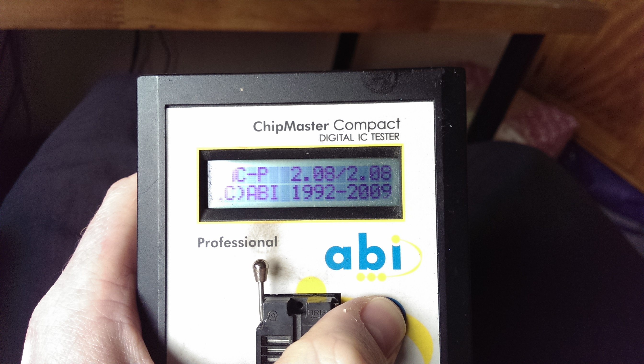
BEFORE:
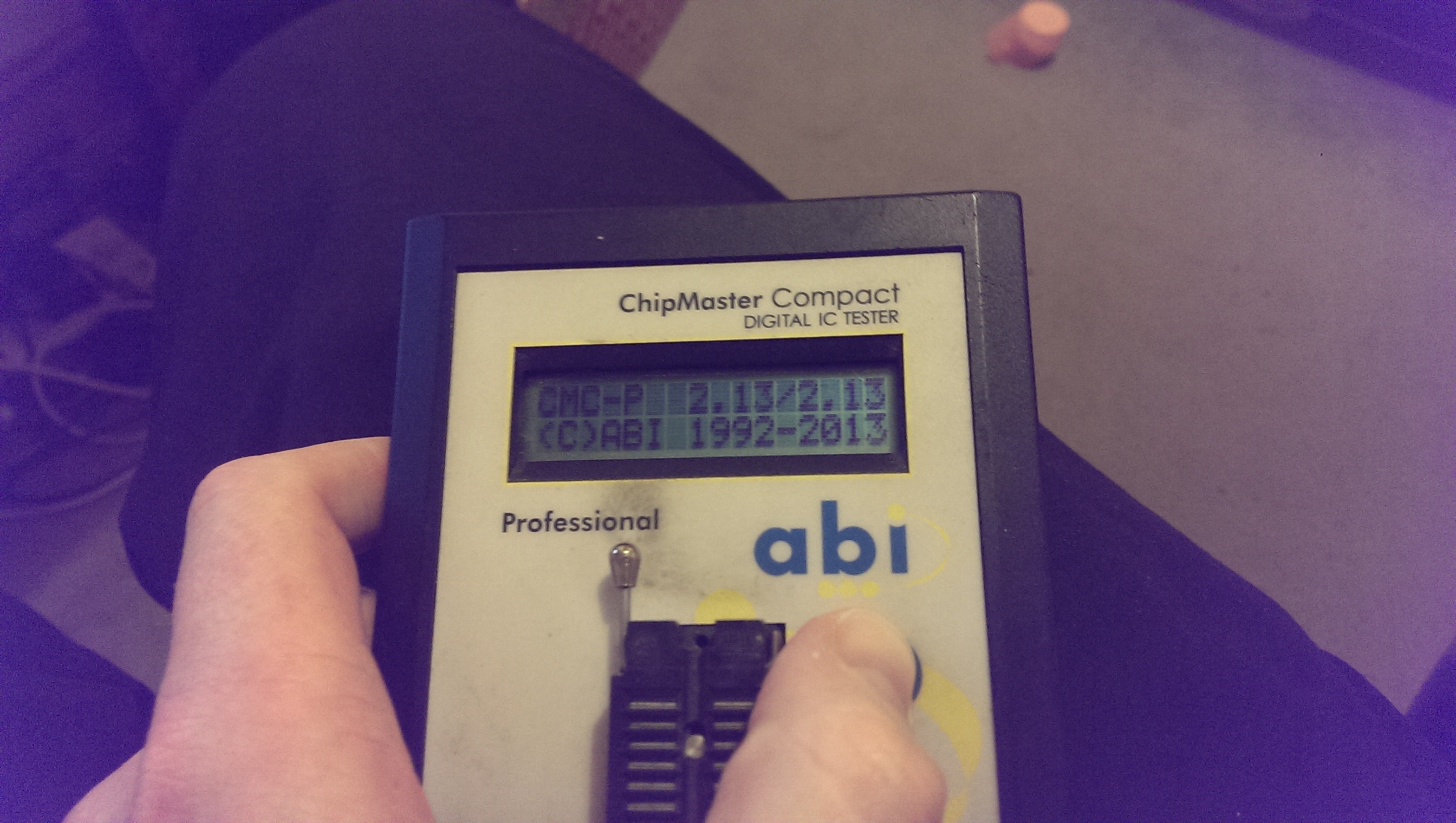
AFTER:
Now I have the software file Im going to pull this thing to bits in IDA Pro and see what interesting things I can find, maybe its even possible to fix the Z80 testing function that ABI cant be bothered to fix themselves.
PAL UpdatesComments Off on Wonder 3 (Japan 910520) PAL dump added
Feb152015
Today I converted to GAL16V8 the binary PAL dump ‘rt22b.1a’ from the MAME ‘wonder3’ set and Silvio Grazini successfully tested it on his CPS1 board.JED was added to database.Thanks both to him and the original dumper.
Got this original Taito/Toaplan Rally Bike PCB for cheap:
Seller claimed that it was working fine except that it didn’t coin up with both players.So, I was confident that it would have been an easy repair (but in hindsight I can say not really..).
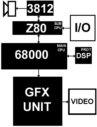
When I started my troubleshooting I found none of the inputs (and dispwitches, too) were working.Checking all JAMMA connector pins with a logic probe revealed they were all fine (high when input is not activated and low when button/direction switch is pressed) so resistors arrays were doing their job but something happened after and the signals could be not propagated.Tracing back the inputs I found that they were tied to inputs of some 74LS240 near the JAMMA connector.Probing them revealed that outputs didn’t change they state when inputs were activated because all the enable pin (PIN1 and PIN19) were stuck high.All these enable signals were tied to some outputs of a 74LS138 which I tested good out-of-circuit.So, I was in a dead end and giving up but doing some research about Toaplan hardware I came across this page:
where it said that Z80 audio CPU handles not only sound control but also all I/O reading:
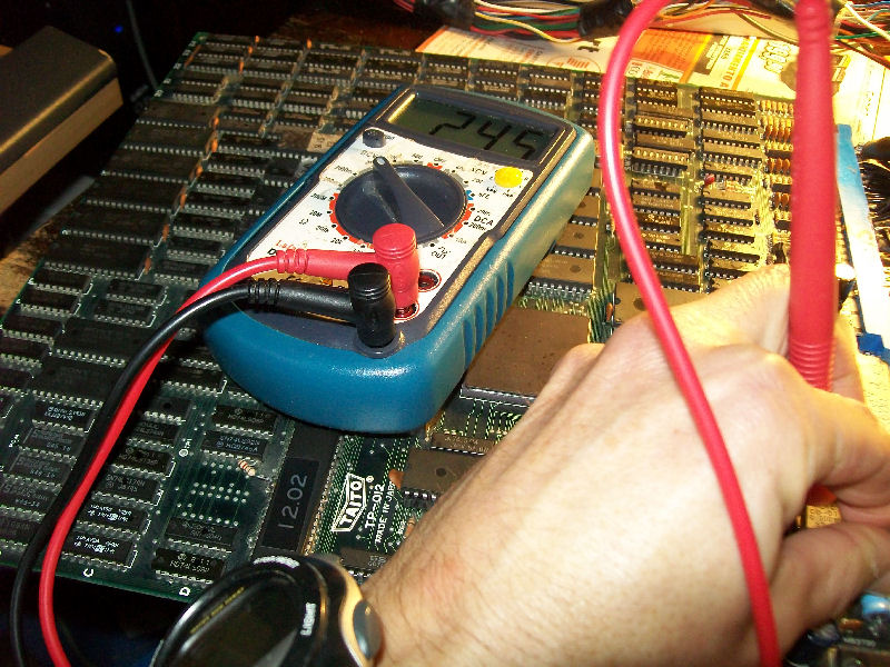
So I started to probe the digital audio circuit and found thath some address lines of Z80 (and so also of the connected RAM/ROM) were stuck low as well all data lines of the YM3812 sound synthesis chip were in high impedance state due the /CS pin stuck high.The audio ROM was dumped fine and piggybackinbg the 6161 RAM had no changes at all but when I made it over the YM3812 suddenly the game coined up and started a game.I swapped it for a good one and all the inputs were working again.But sound was totally missing, only some hissing noise sign that the main MB3730 amplifier was good at least.Since digital part of audio circuit was fine, the fault was located in analog section.Probing the YM3014 DAC and the LM358 OP-AMP I could measure only 2.45V across their power pins sign that there was almost a short on thes two ICs:
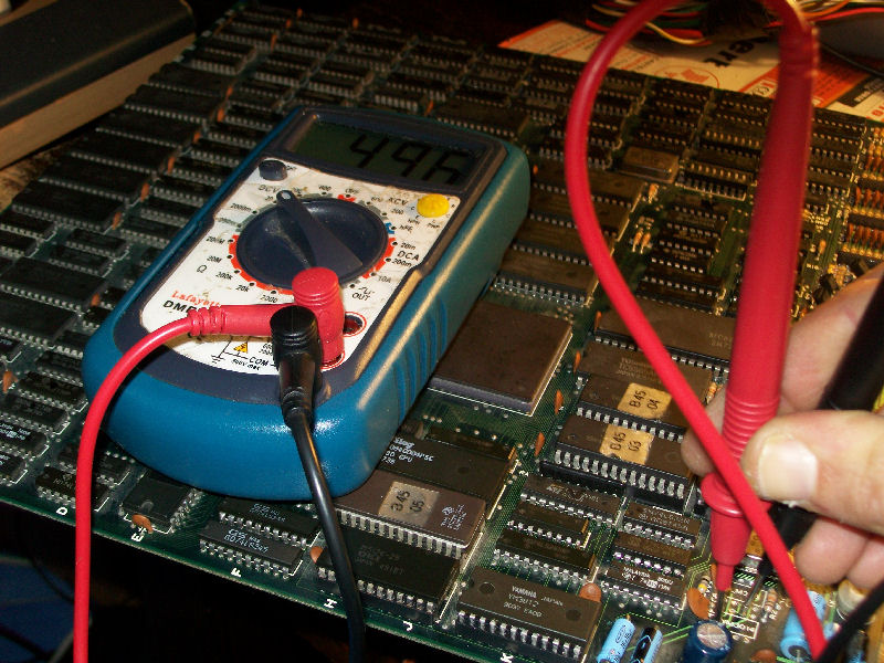
Infact, after removing them, I could measure the right voltage on the power pads:
Replaced both YM3014 and LM358 restored full sound.End of job.