Konami 007644 custom chip

 General, Technical Info  Comments Off on Konami 007644 custom chip
Jun 132014
 

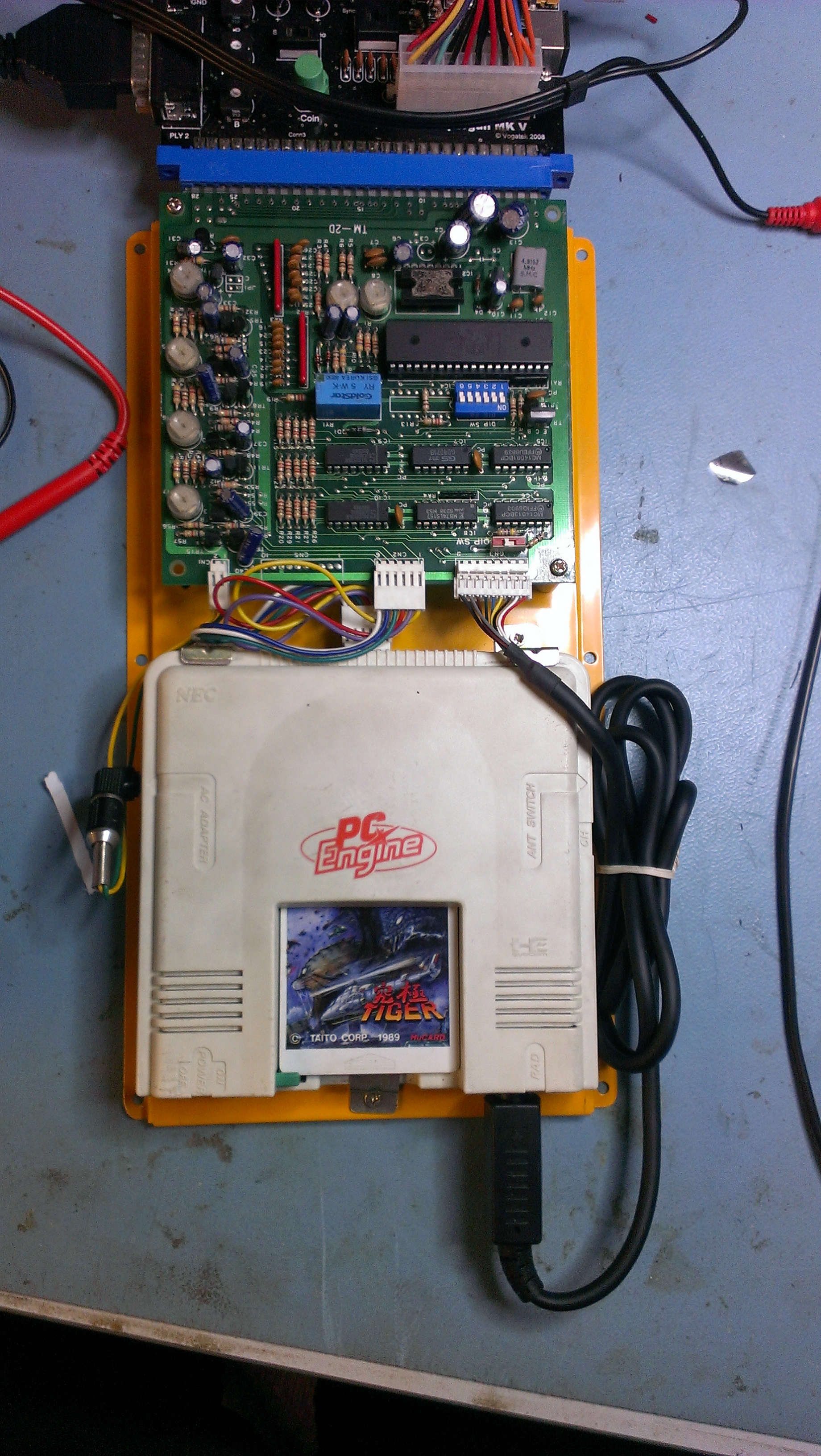
Ive got a board that needs a new 007644 custom chip.
While im waiting to find a new one I thought I would investigate how this chip actually works.

Pin 1 = SEL – changes whether the Q outputs require a rising edge clock or not.
Pin 2 = OEY – Output enable for the Y outputs else they are inputs. Active LOW
Pin 21 = OEQ – Output enable for the Q (clocked) outputs else they are inputs. Active LOW
Pin 12 = CLK – Clock input

Pins 3-10 = Y outputs – normal outputs. If OEY is LOW these pins become outputs mirroring the state of the Q input pins. SEL and CLK pins are not used in this mode.

Pins 13-20 = Q outputs – clocked outputs. If OEQ is LOW these pins become outputs. If SEL is HIGH and CLK is HIGH these outputs will mirror the state of the Y inputs. If SEL is LOW then the outputs will only change state on a rising edge CLK.

Pretty simple and should be easy to implement in a small CPLD if ever required (next project???)

AAA16K4P RAM chips

 General, Technical Info  Comments Off on AAA16K4P RAM chips
Mar 082014
 

A few weeks ago there was a post on KLOV asking what these chips were.
One of the replies to this was that they might be a PAL chip so my attention was caught.
I managed to borrow a PCB pretty quickly and determined that this was not a PAL chip.
A few users had already mentioned that the manufacturer made RAM chips and after doing some circuit drawing I found what type of RAM it is.
If you ever need to find a replacement for the above chip then look for MB81C68.

DOWNLOAD DATASHEET

 Posted by at 7:32 pm

PC Engine -> JAMMA PCB

 General, Technical Info  Comments Off on PC Engine -> JAMMA PCB
Oct 062013
 

A little while back muddymusic lent me his PCE-JAMMA unit to look at.
The whole saga can be found here.

There is pretty much no documentation available out there for this unit but my friend Tormod seems to have quite a bit. Here is a scan of the manual he has for it

After tracing the hardware out and various trials and a fair amount of input from the arcade community we came up with this:

Its not a bad system really and it works well for what it is

 Posted by at 8:38 am

Silent Scope RTC data information

 General, Technical Info  Comments Off on Silent Scope RTC data information
Dec 182012
 

Today I burned a new Timekeeper chip for someones Silent Scope and since I had my board out for testing I thought Id run a few tests of my own.
I know with SS2 there is a checksum in the RTC data. This is not the case with SS1. It just has 13 bytes of data not all of which gets checked.
Here is what I found:

The first 8 bytes must read: 47 51 38 33 30 00 00 00 (GQ830 )
If any of this is different then you will get the 11p error

The next 2 bytes are the year. Mine originally read 20 00
It is actually the year thats shown in game on the title screen etc and can be changed to whatever you want, like this

The last 3 bytes must read: 55 41 41 (UAA). If this is changed to anything else then its 11p error time again.

From what ive tried you can add any data after this and it will make no difference.
The same data is also used across all versions of Silent Scope 1.

I will take a look at the SS2 data sometime too.

 Posted by at 1:39 pm

Data East ’59’ 68000 CPU Info

 General, Technical Info  Comments Off on Data East ’59’ 68000 CPU Info
Dec 082012
 

Ive been attempting to create a pinout of that 68K. I’m pretty sure what I’ve got so far is accurate although I make no promises as it does get a bit confusing sometimes. If you can shed any light on the pinout of this chip I would be grateful.

—CUSTOM 68K—
pin 7 = A1
pin 8 = A2
pin 9 = A3
pin 10 = A4
pin 11 = A5
pin 12 = A6
pin 13 = A7
pin 14 = A8
pin 15 = A9
pin 16 = A10
pin 17 = A11
pin 18 = A12
pin 19 = A13
pin 20 = A14
pin 21 = A15
pin 22 = A16
pin 23 = A17
pin 24 = A18
pin 25 = A19
pin 26 = A20
pin 28 = A21

pin 27 = VCC
pin 54 = VCC
pin 55 = VCC
pin 56 = VCC
pin 64 = VCC

pin 31 = GND
pin 58 = GND

pin 32 = D7
pin 33 = D6
pin 34 = D5
pin 35 = D4
pin 36 = D3
pin 37 = D2
pin 38 = D1
pin 39 = D0
pin 40 = D15
pin 41 = D14
pin 42 = D13
pin 43 = D12
pin 44 = D11
pin 45 = D10
pin 46 = D9
pin 47 = D8

pin 48 = AS
pin 49 = UDS
pin 50 = LDS
pin 51 = R/W
pin 52 = DTACK

pin 57 = CLK

This post will be updated with any new information if/when I get it.

 Posted by at 12:07 pm