Had Muddymusic’s Stun Runner PCB for a long long time awaiting repair.
I put off looking at it because of how test bench unfriendly it would be to setup.
I did have most of the original loom to use but the audio section also used 13v AC and a test bench typically doesn’t have that.
I ordered a small 240v – 12v transformer and eventually set to work in hooking this thing up.
After half a day of messing around I had what I thought was a Stun Runner test rig.
While I had all the connections going to the right places and things like that I soon realised that the speakers I were using in now way suitable to check the sound and also my test bench monitors seem to be getting really picky about what they display properly.
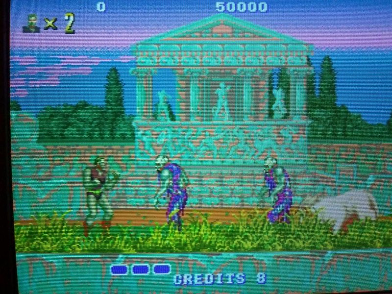
In the end I settled for a black and white picture but I wasn’t too worried as the fault I was looking for was audio related.
The fault was that in game the music didn’t play and the engine tone played at a constant tone.
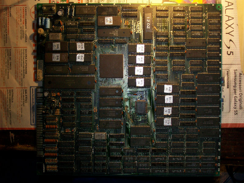
With my almost useless setup I could hear exactly this. I did a quick heat check with my finger on the audio PCB to check if any of the chips were getting hot and to my surprise all the sounds and music came back when I prodded the M6295.
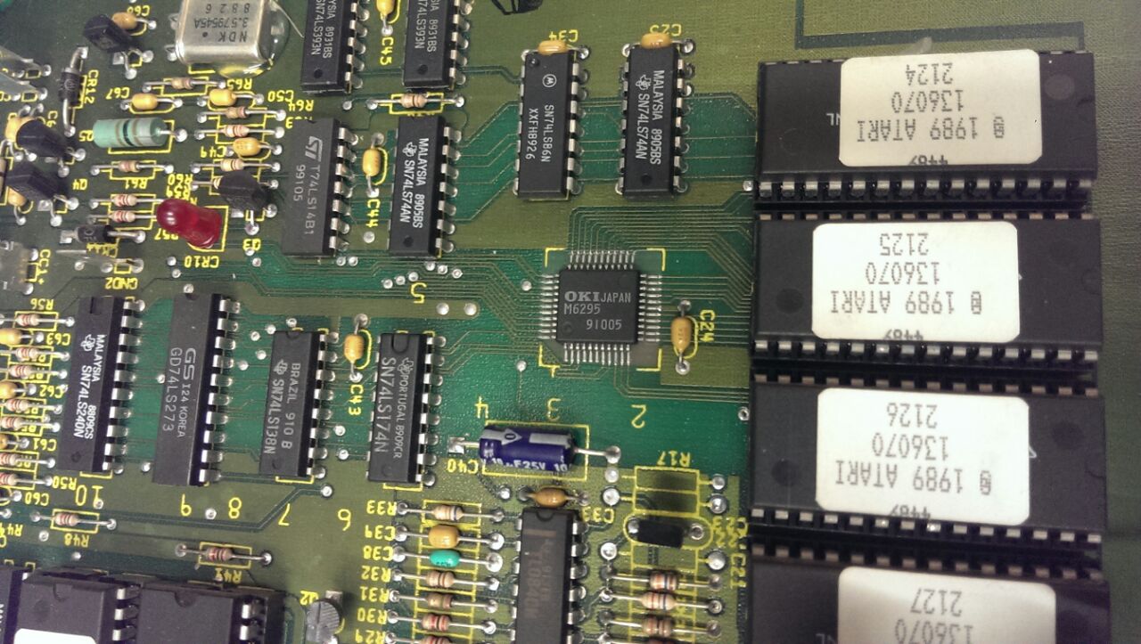
I powered down and reflowed the chip and all was working again.
I soak tested it as best I could and called it a day.
Muddymusic has now got it back and has confirmed the sounds and music are now good.