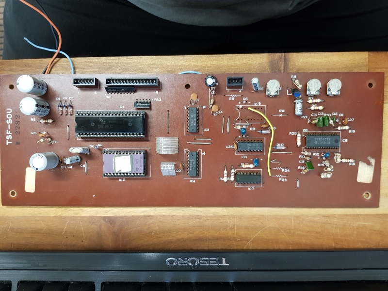
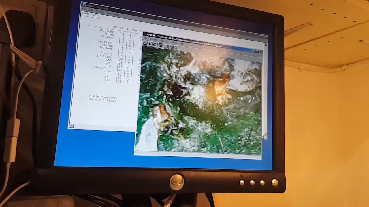
I got this Bombjack Bootleg board a while back when I just couldn’t find any original boards for my cab. I since got an original board for it but this bootleg has been left for repair since then.
It was sold as “graphic & sound issues” without more explanations. Lucky though, these bootlegs are identical to the original boards.
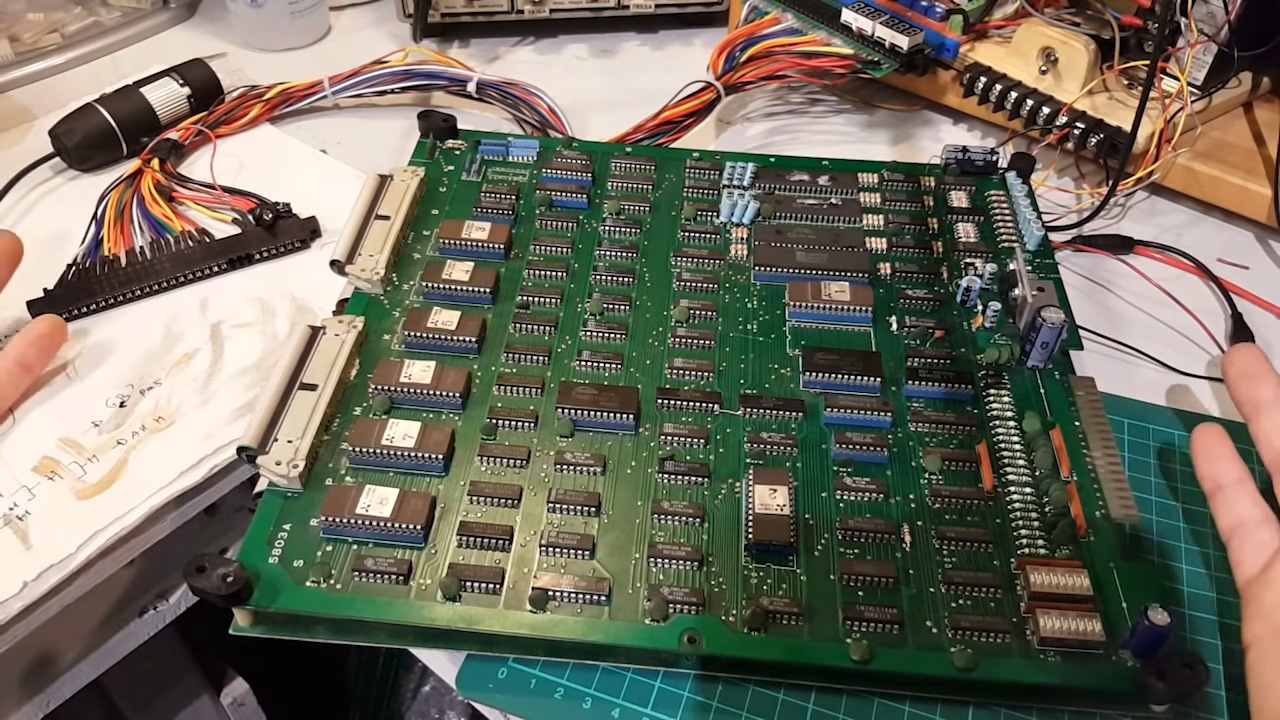
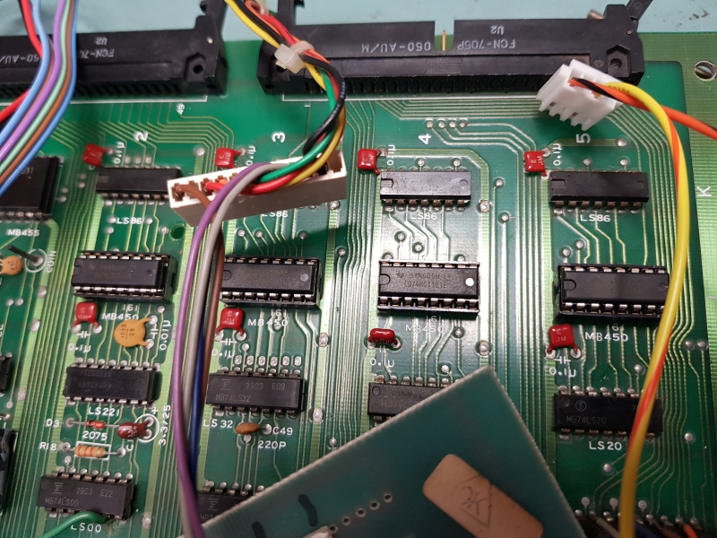
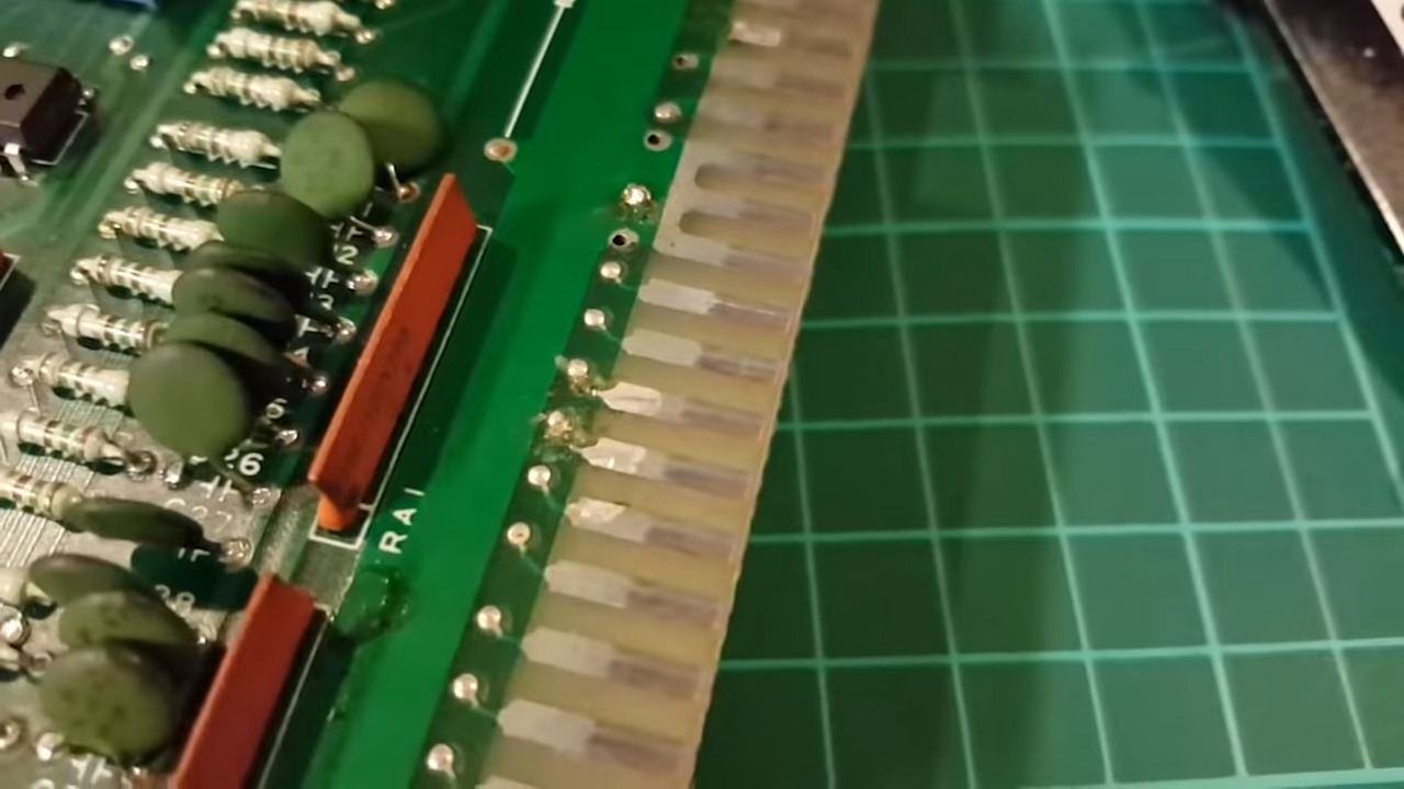
A first visual inspection reveals a few loose & broken filter capacitors and a couple of messy traces near the edge connectors. Hard to say without a magnifier if they’re broken. The caps won’t be an issue for now so let’s focus on the traces
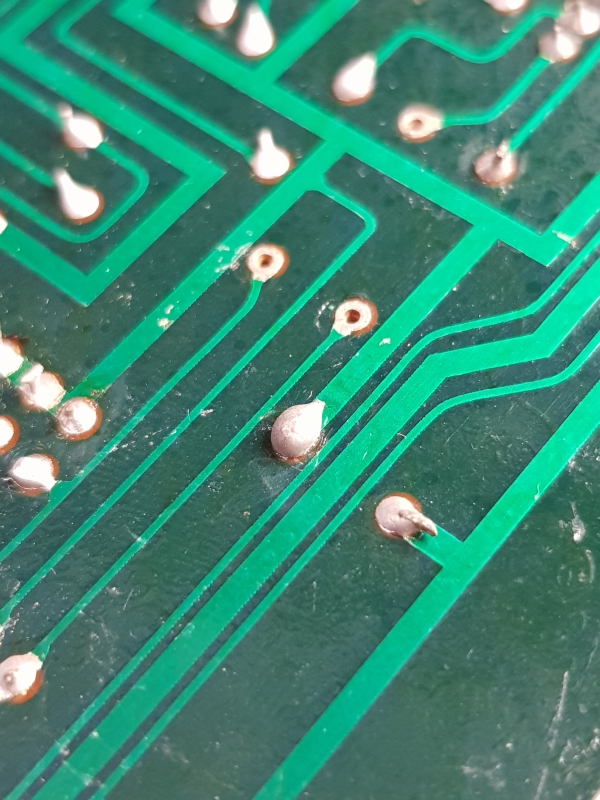
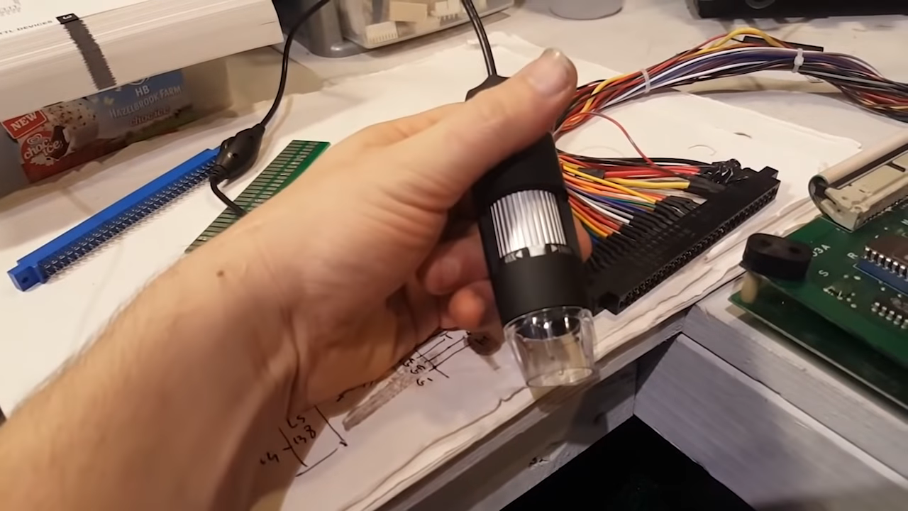
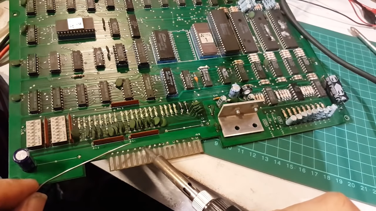
I could do a quick continuity test but as it happens, somebody sent me one of those cheap chinese microscope things. They’re essentially a USB webcam , so this is a good opportunity to give it a test.
Indeed two traces were broken, a quick solder bridge will fix that. Handy little toy that thing!
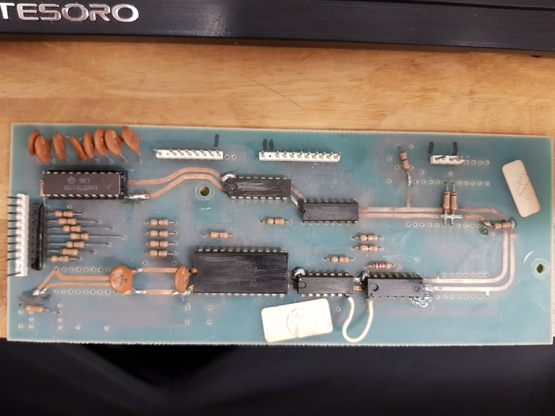
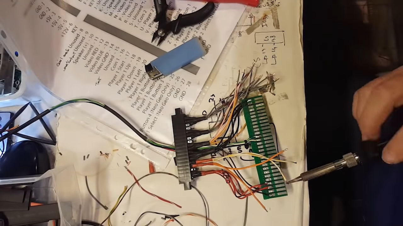
Next, I had to make an adapter since the board didn’t come with one.
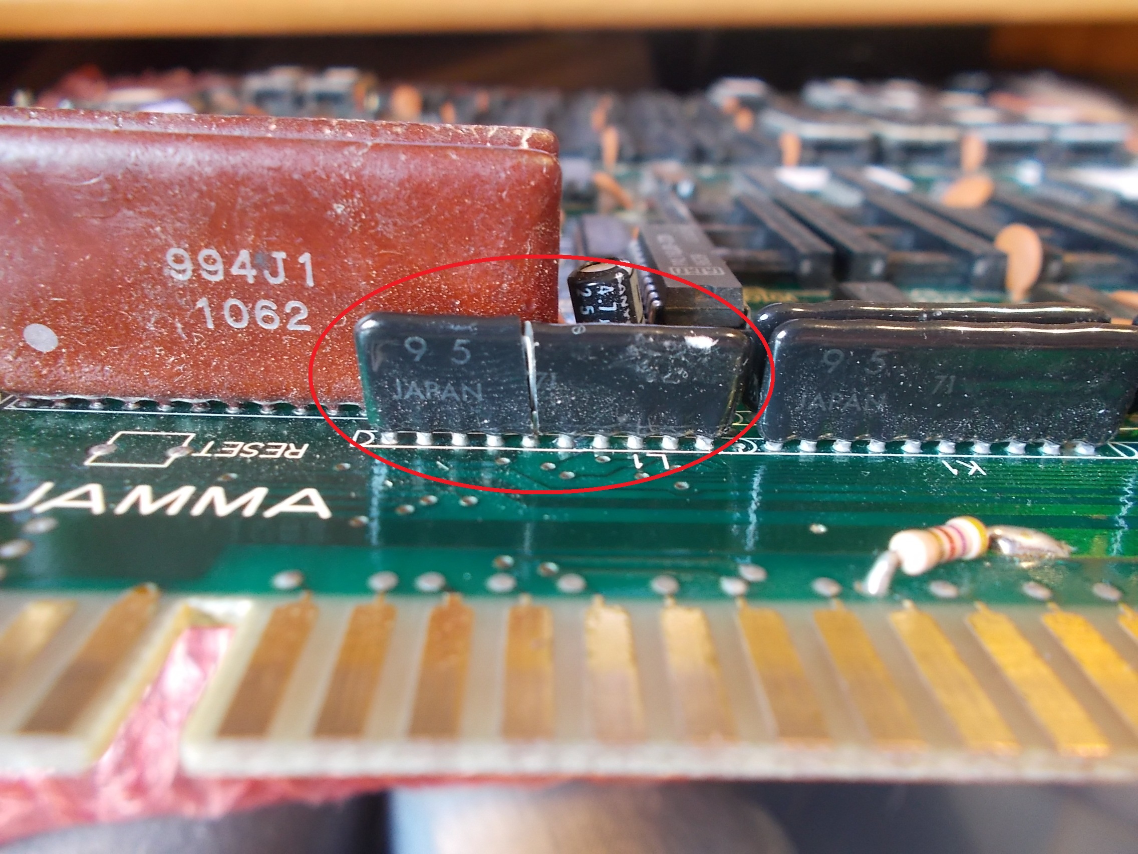
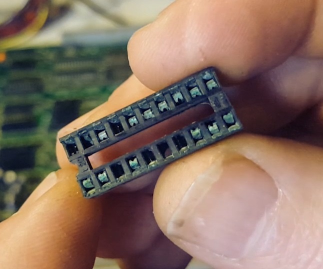
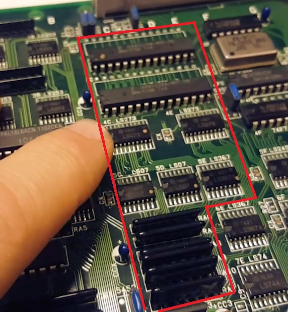
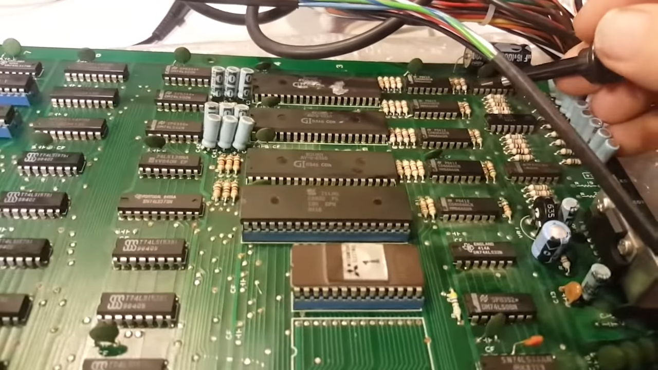
On these boards the video signal comes from a separate connector on the far edge of the board. You can already spot there’s an IC missing there too
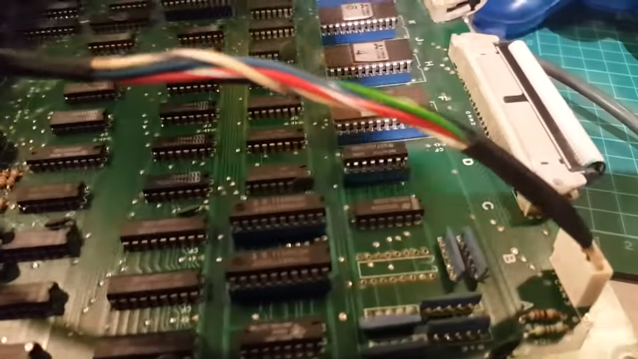
This might explain the graphic issue.
But first let’s finally power the board and check what we get.
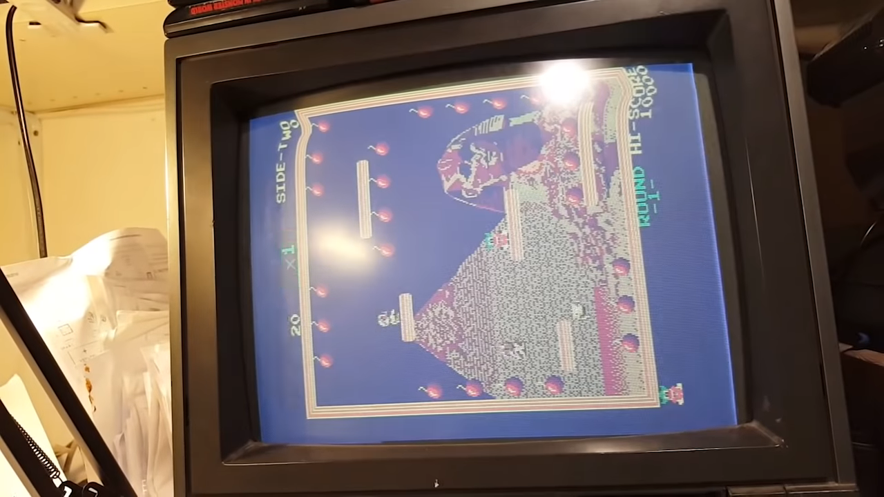
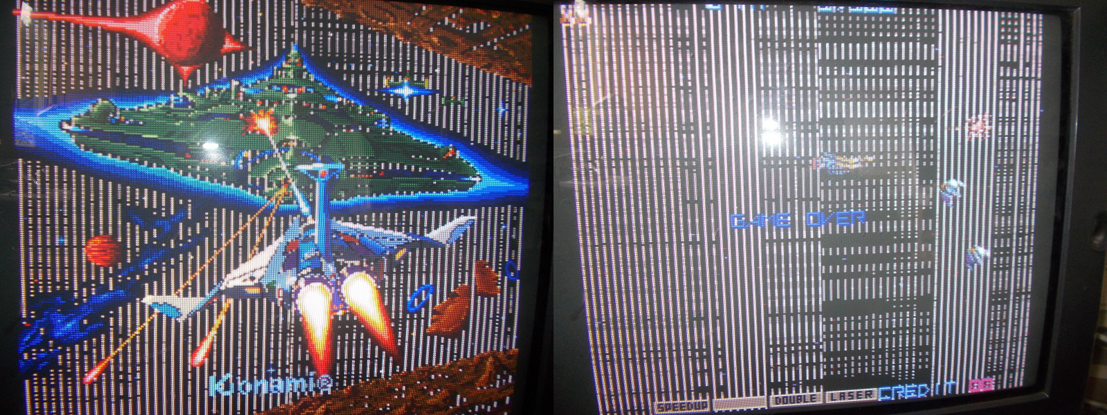
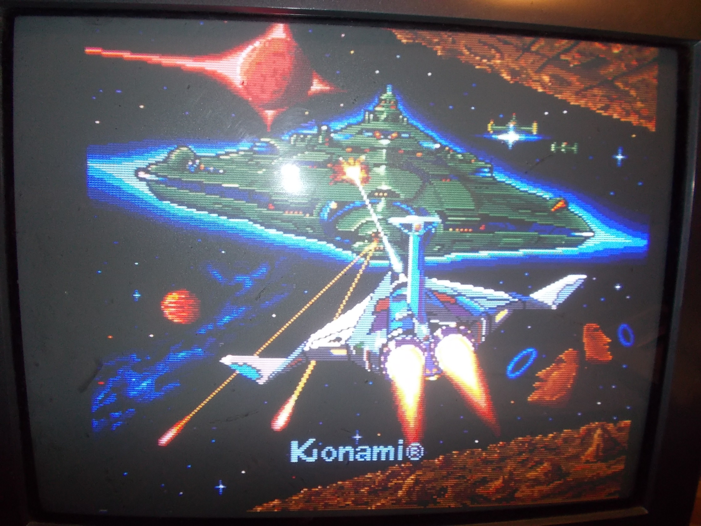
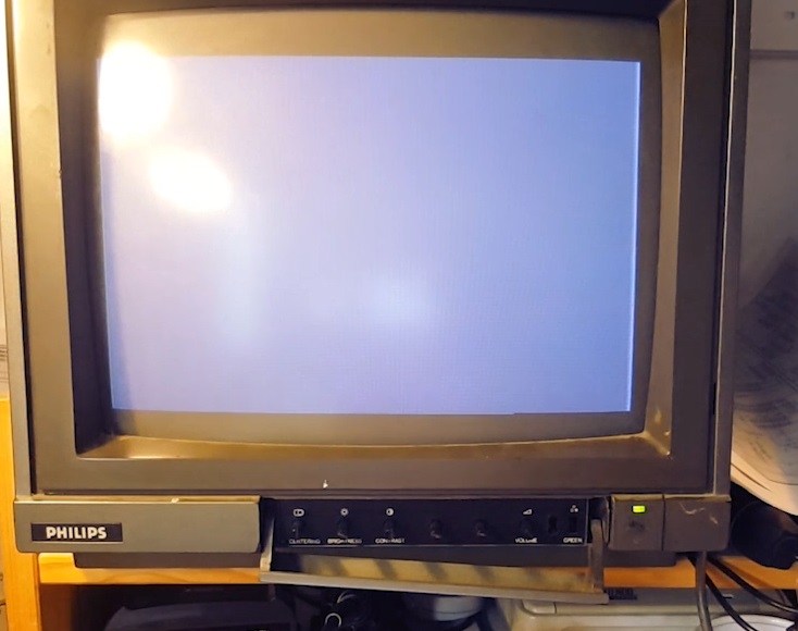
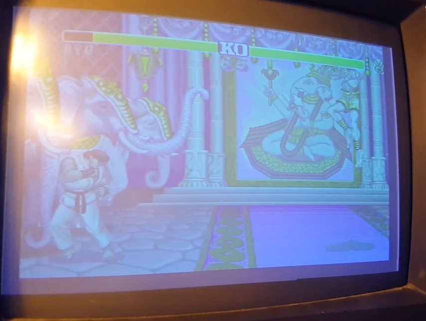
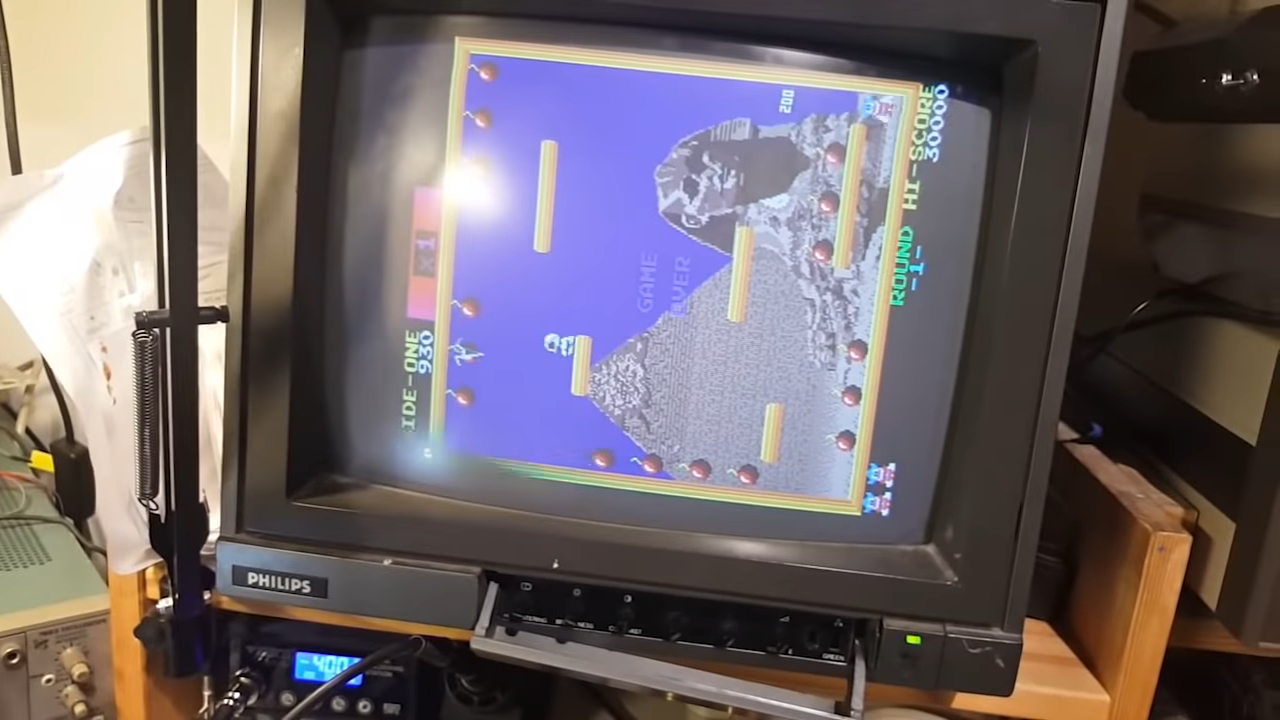
So our colors are off, some graphic information is missing. There’s no sound coming from the board either. The wavy effect on top of the screen is an artifact of my monitor being in need of a re-cap so we can ignore this.
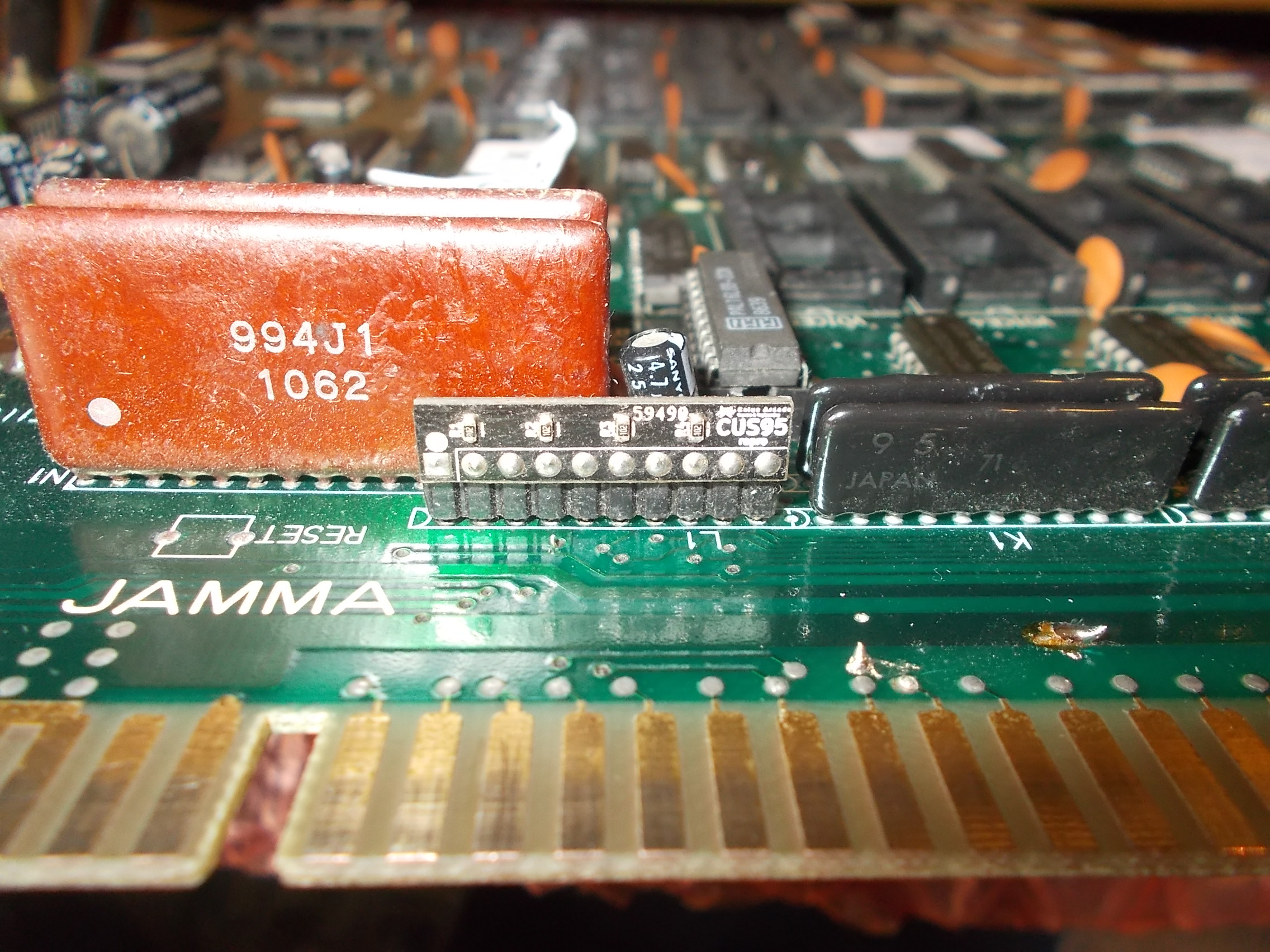
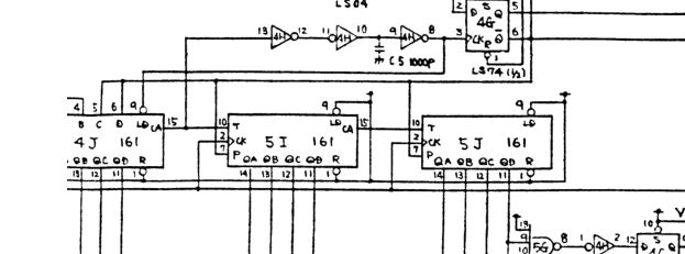
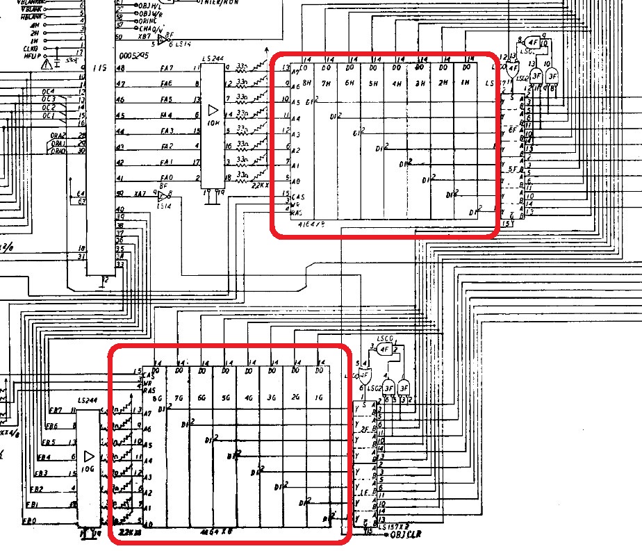
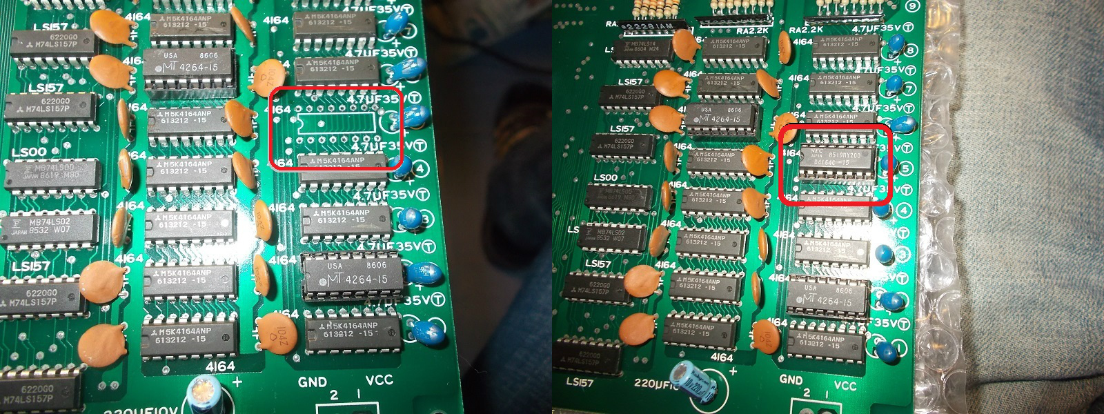
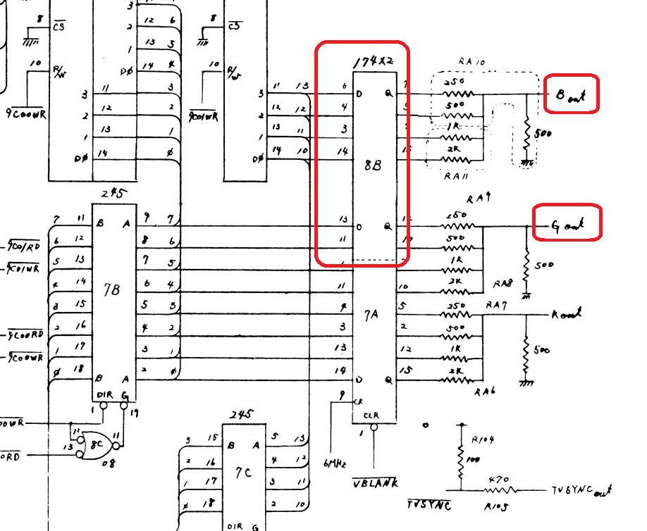
Let’s first take care of that missing IC. Looking at a photo found online, this should be an LS174 flip-flop.
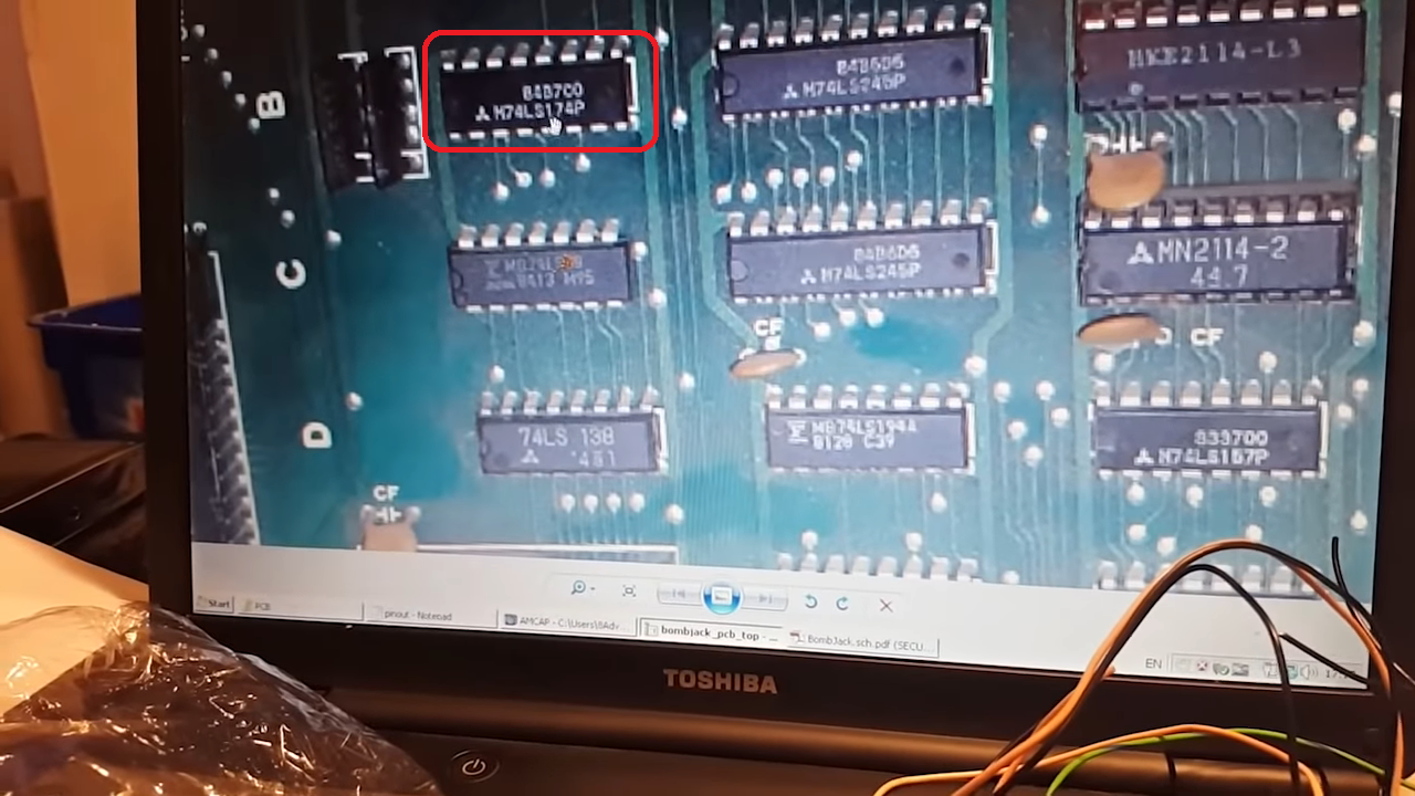
I then checked the schematics and this confirms it as a pair of these is handling the color signals. Our missing IC at 8B handles the blue and part of the green signal.
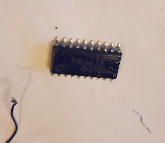
Let’s drop a fresh one and see if this restores our picture.
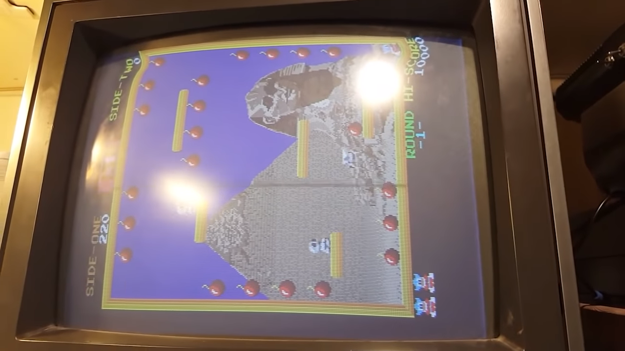
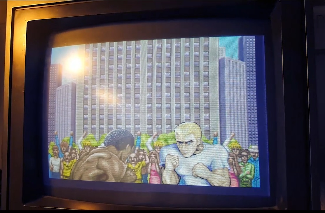
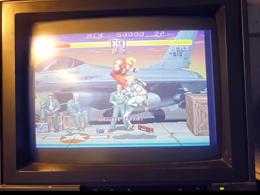
Success!!
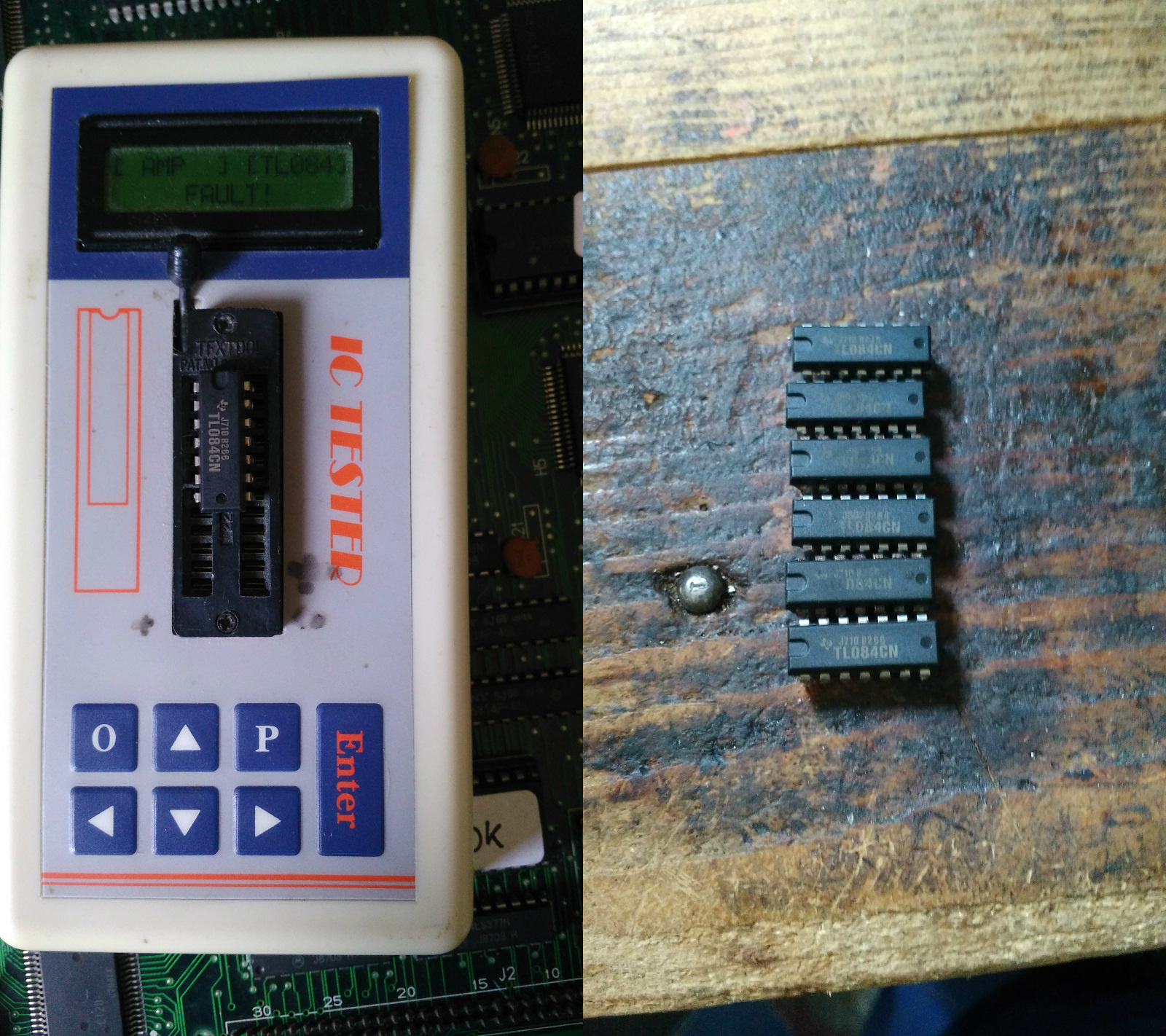
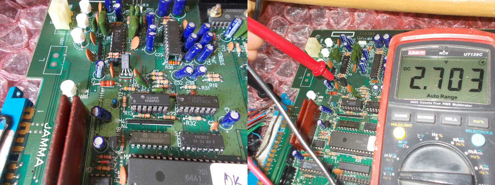
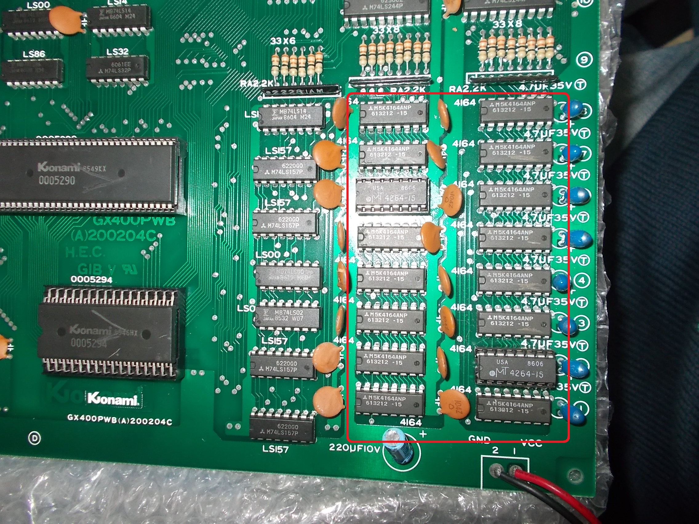
Now to address the sound issue. Probing my way from the amp back I eventually realized I’was not getting any signal. All outputs on the sound ICs (three AY-3-8910) were dead , I suspected the z80 controlling these.
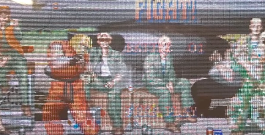
Swapping it with a new working one restored the sound completely board … here’s a photo for proof :
In addition to this I did make a couple of mistake on my adapter, meaning the controls worked incorrectly. I spent some time trying to troubleshoot this till I double checked my adapter. ah well. Another case where having another working set would prove useful.
Anyway the board is working fine now, but while I tidied a few loose capacitors around the board I spotted this unpopulated section of the bootleg board:
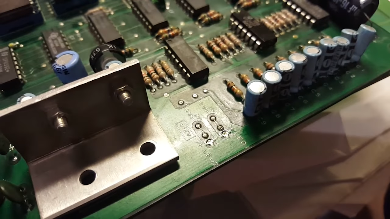
Silk screen and holes for two leds and resistors. Comparing to an original board and checking the schematics, these should be indicators for the 5v and 12v lines.
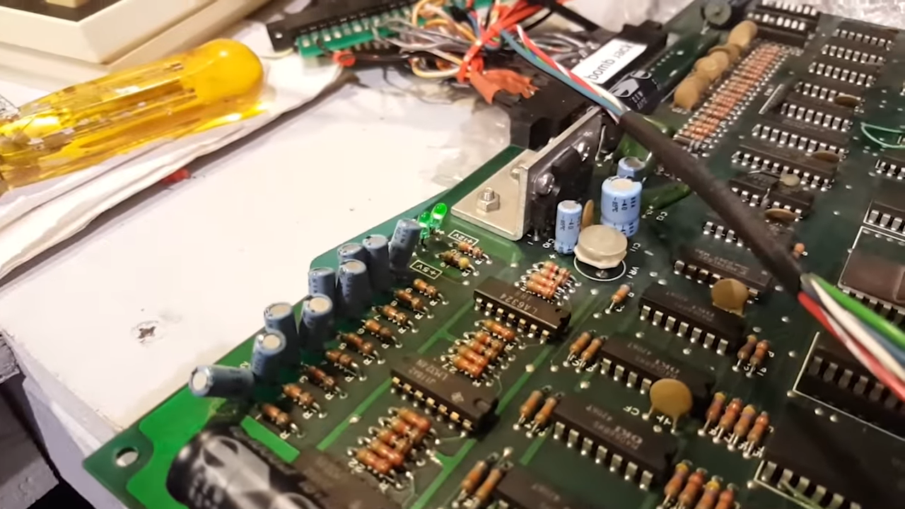
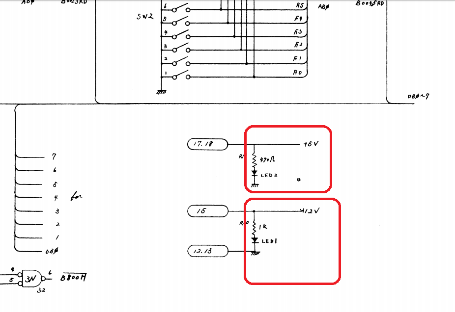
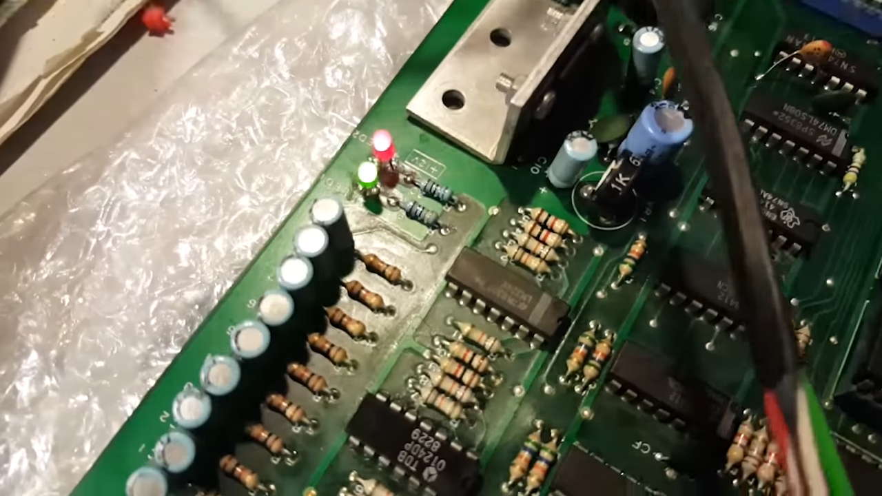
While this is not strictly needed it’s an easy thing to just add them . I went for a green 5V and red for 12V
yay . a fully working Bomb Jack bootleg.
And for those preferring the video format: