1942 double repair log

 PCB Repair Logs  Comments Off on 1942 double repair log
Jun 272019
 

I had a couple of original Capcom ‘1942’ PCBs lying around which I never tested due to the lack of a proper JAMMA adapter (game uses an unique pinout which is not the Capcom Classics one).Recently I had chance to build the adapter and try the boards out, it turned out both were faulty.

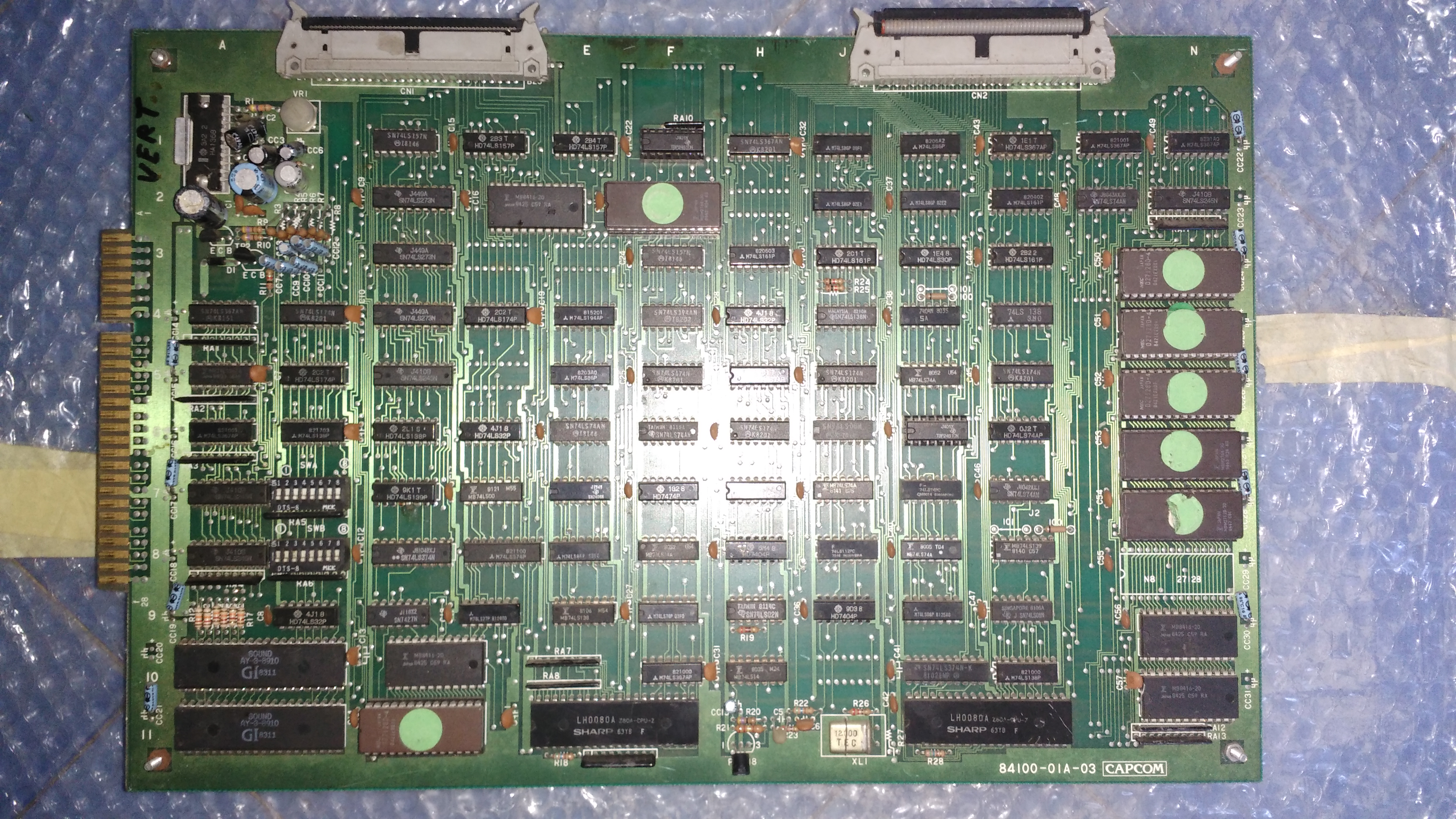
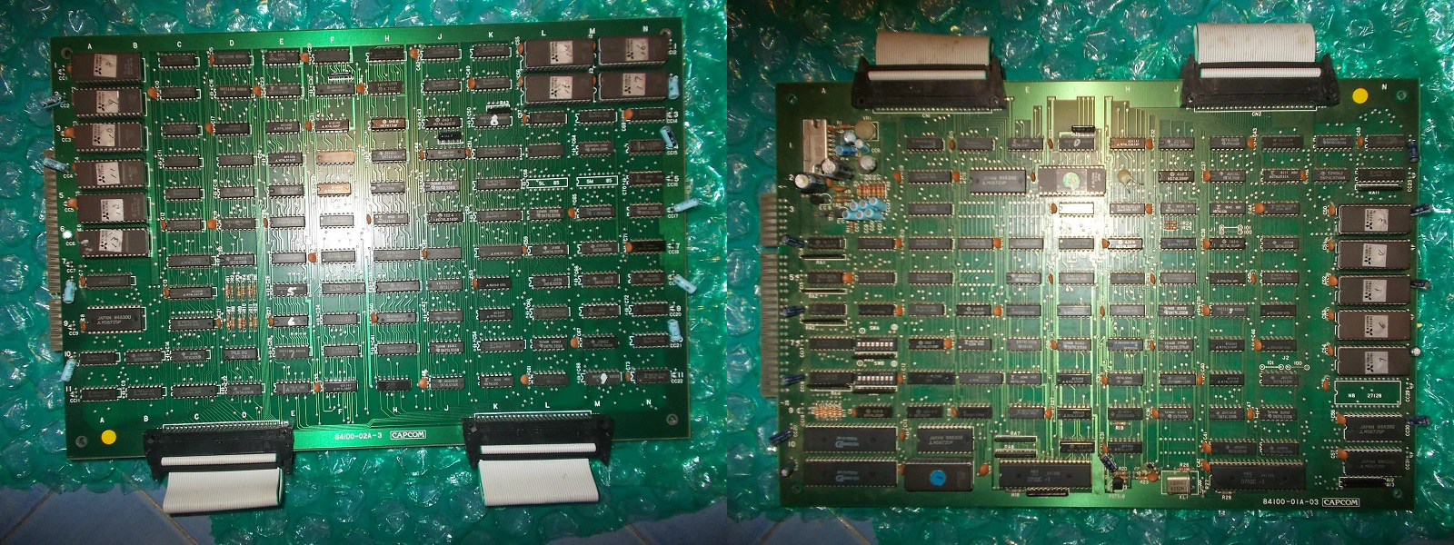
The first set was in good shape in its CPU board :

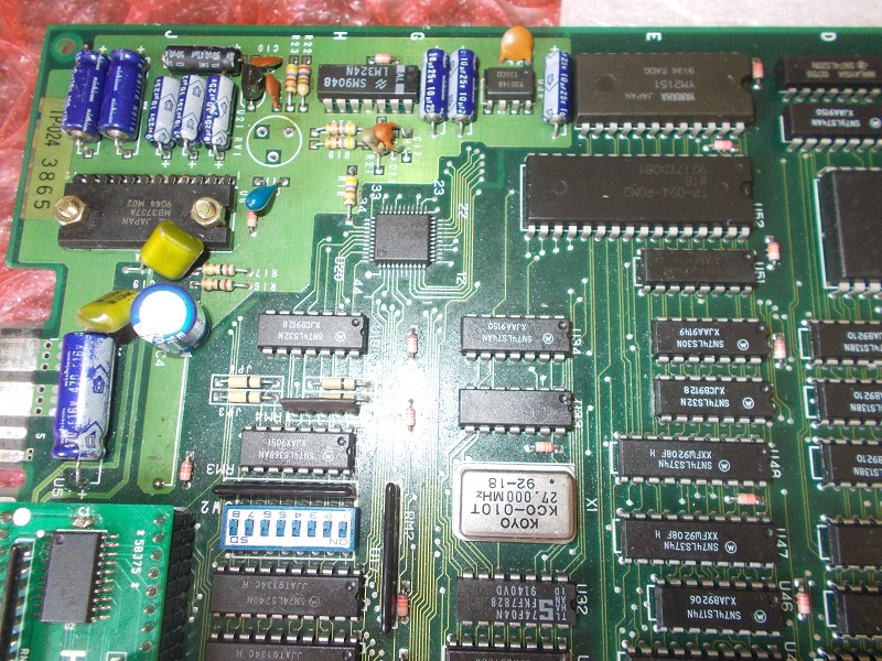
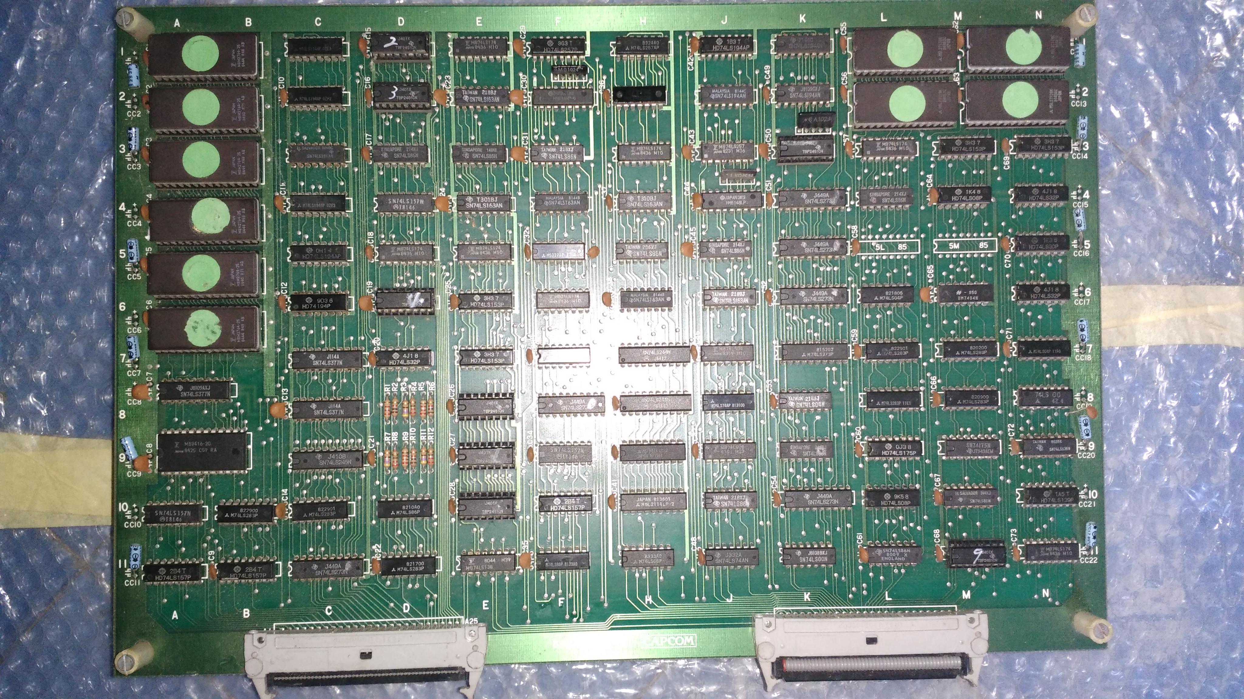
And VIDEO board:

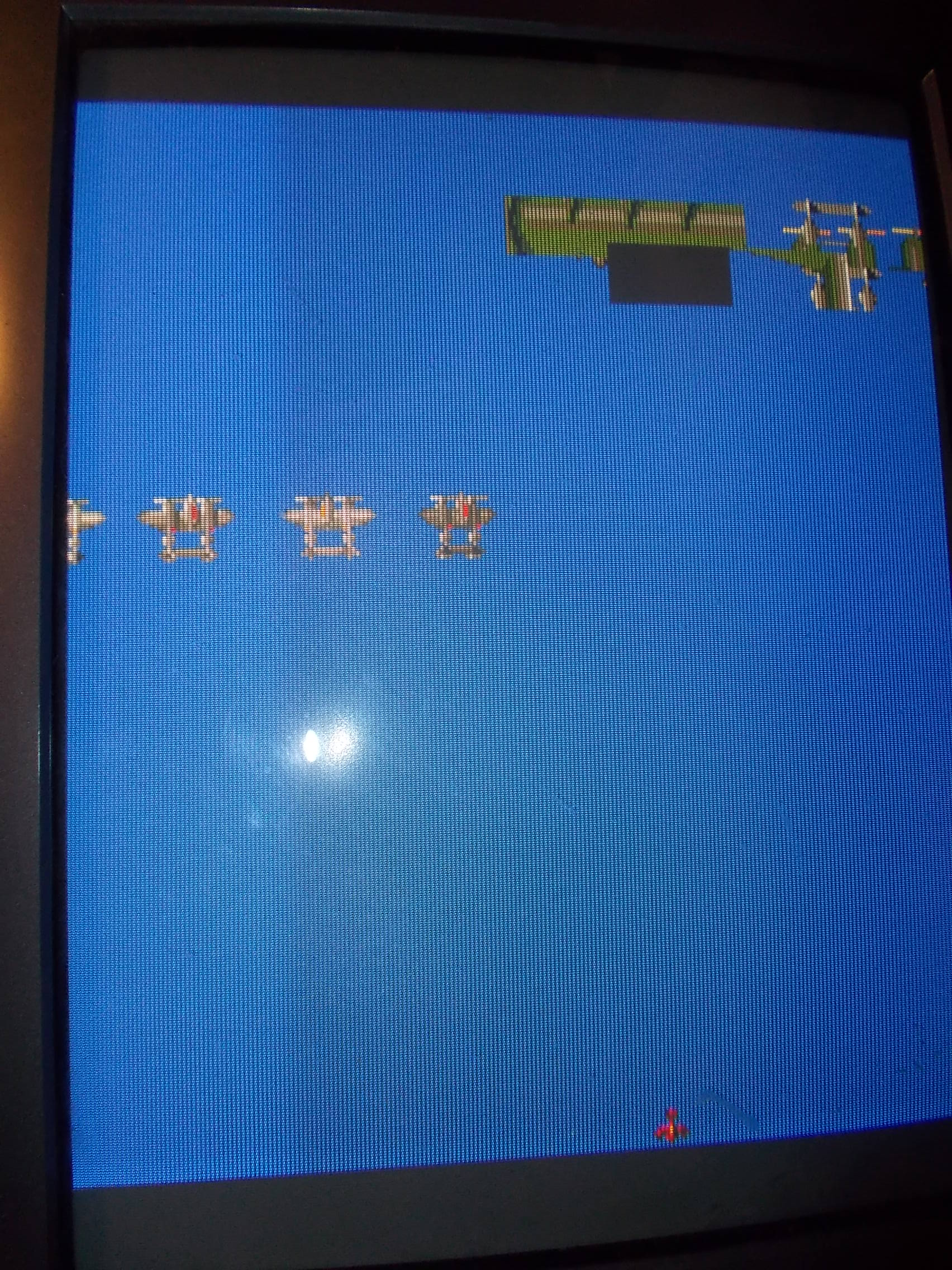
It even booted up and played with sound too but sprites (planes) were totally absent:

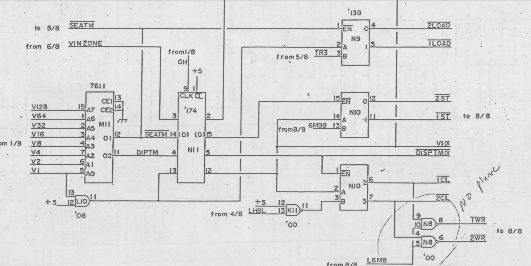
The faulty was obviously located on VIDEO board so I went through schematics and found a part of the object circuit highlighted with an handwritten note saying “NO PLANES”

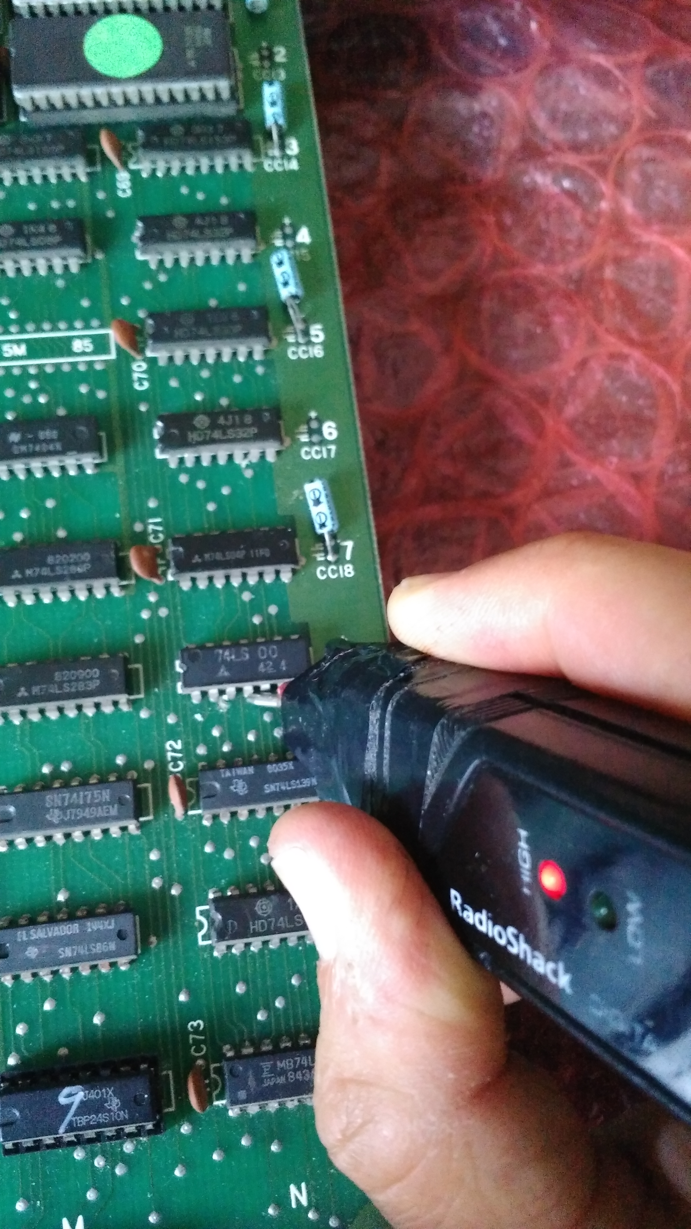
The circled section concerned two NAND gates of a 74LS00 @N8 which generates two signals labeled ‘1WR’ and ‘2WR’.When I probed the inputs I found pin 9 and 4 stuck HIGH:

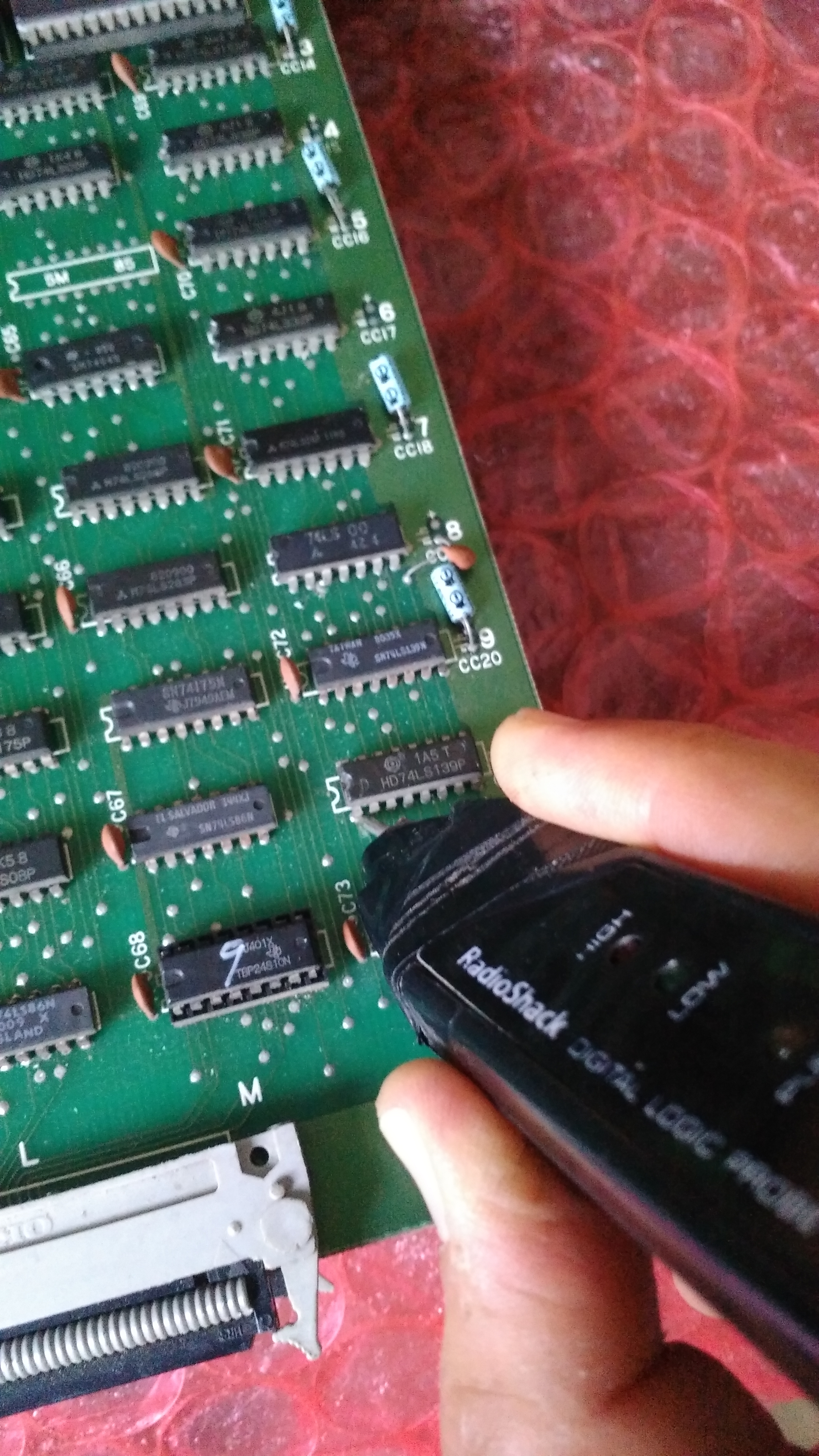
These inputs come from outputs of a 74LS139 @N10 which had its pin 1 floating:

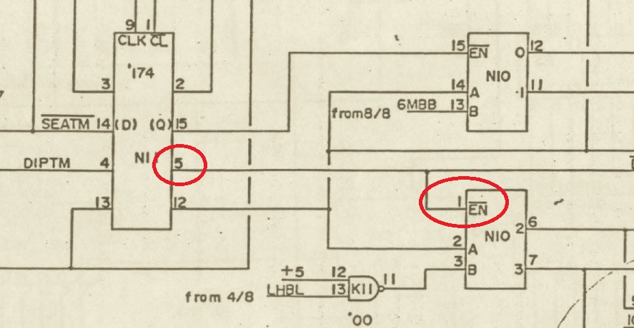
Pin 1 is the enable input of the decoder and comes from output pin 5 of a 74LS174 @N11 :

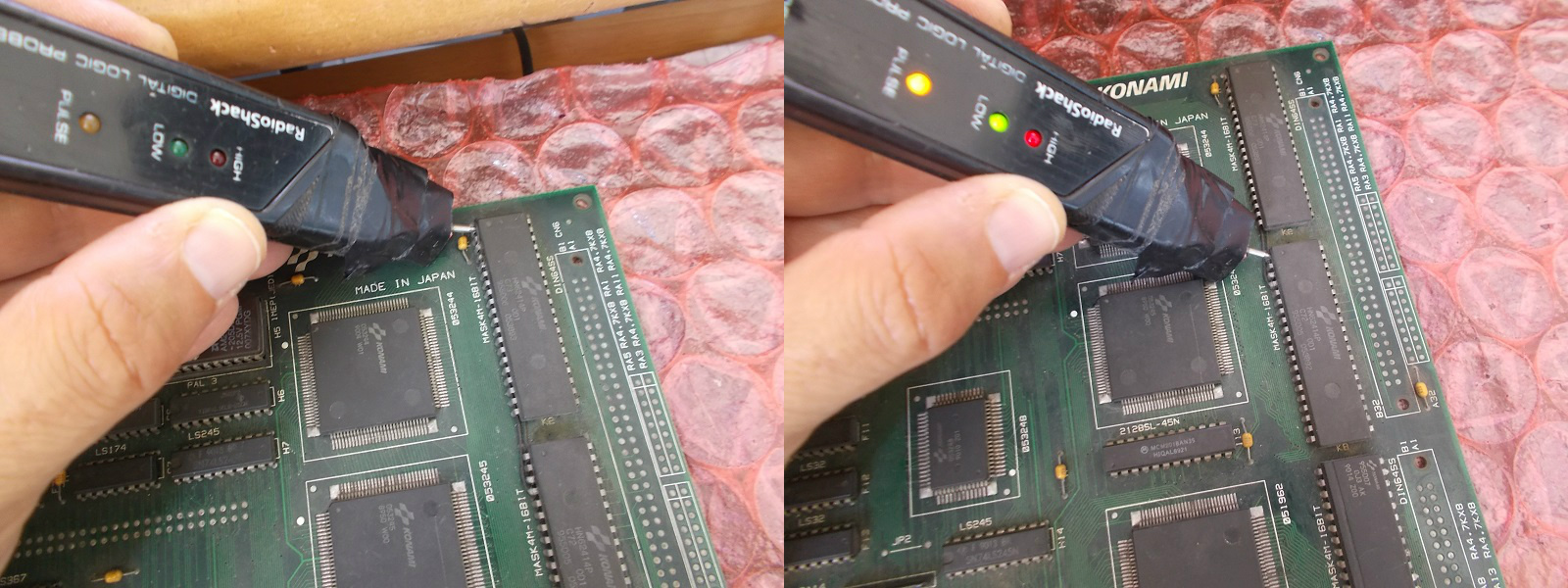
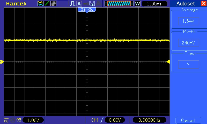
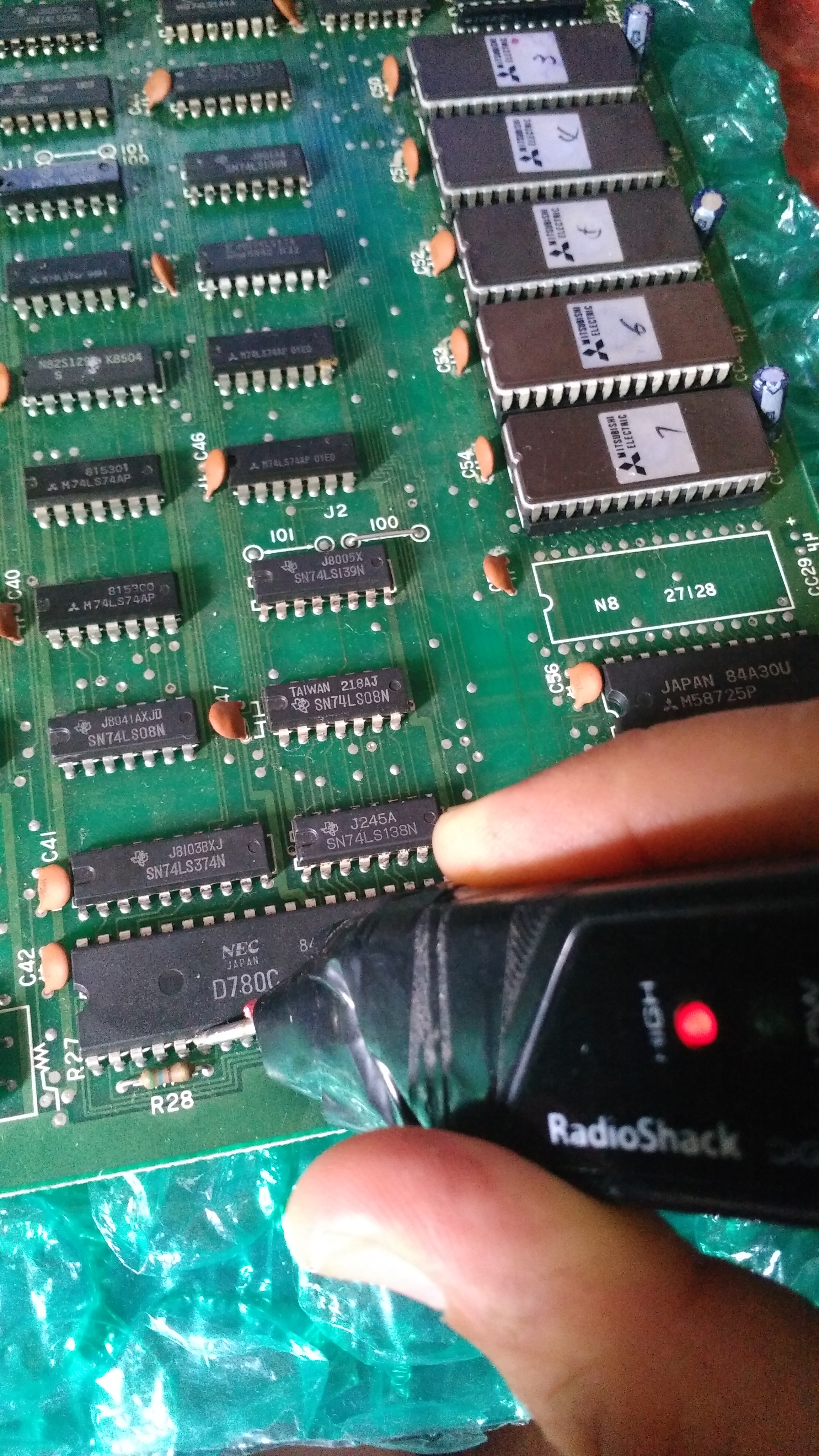
Pin 5 of this 74LS174 was indeed floating, stuck at undefined voltage level of +1.64V :

But the input pin 4 was active :

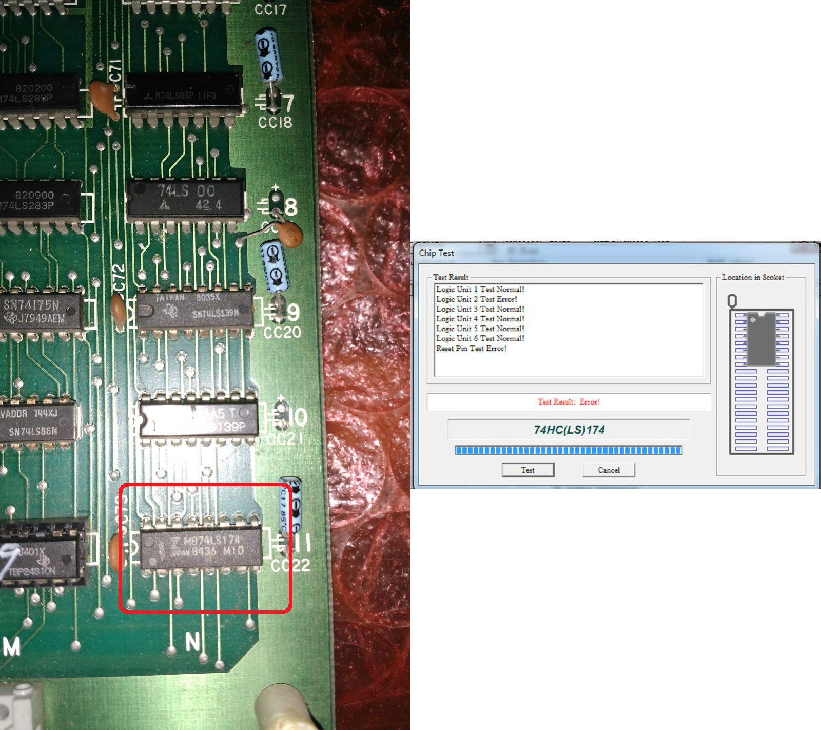
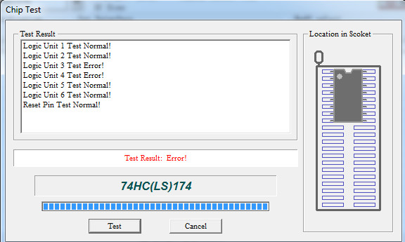
This is a typical way of failure of Fujitsu TTLs and the part was from this manufacturer hence , sure enough, I removed the chip.It miserably failed the out-of-circuit testing:

Replacing it restored the sprites :

First board fixed.


The second set was in good shape too :

But it booted to a static garbage screen :

Probing the Z80 main CPU revealed clock input (pin 6) was stuck high:

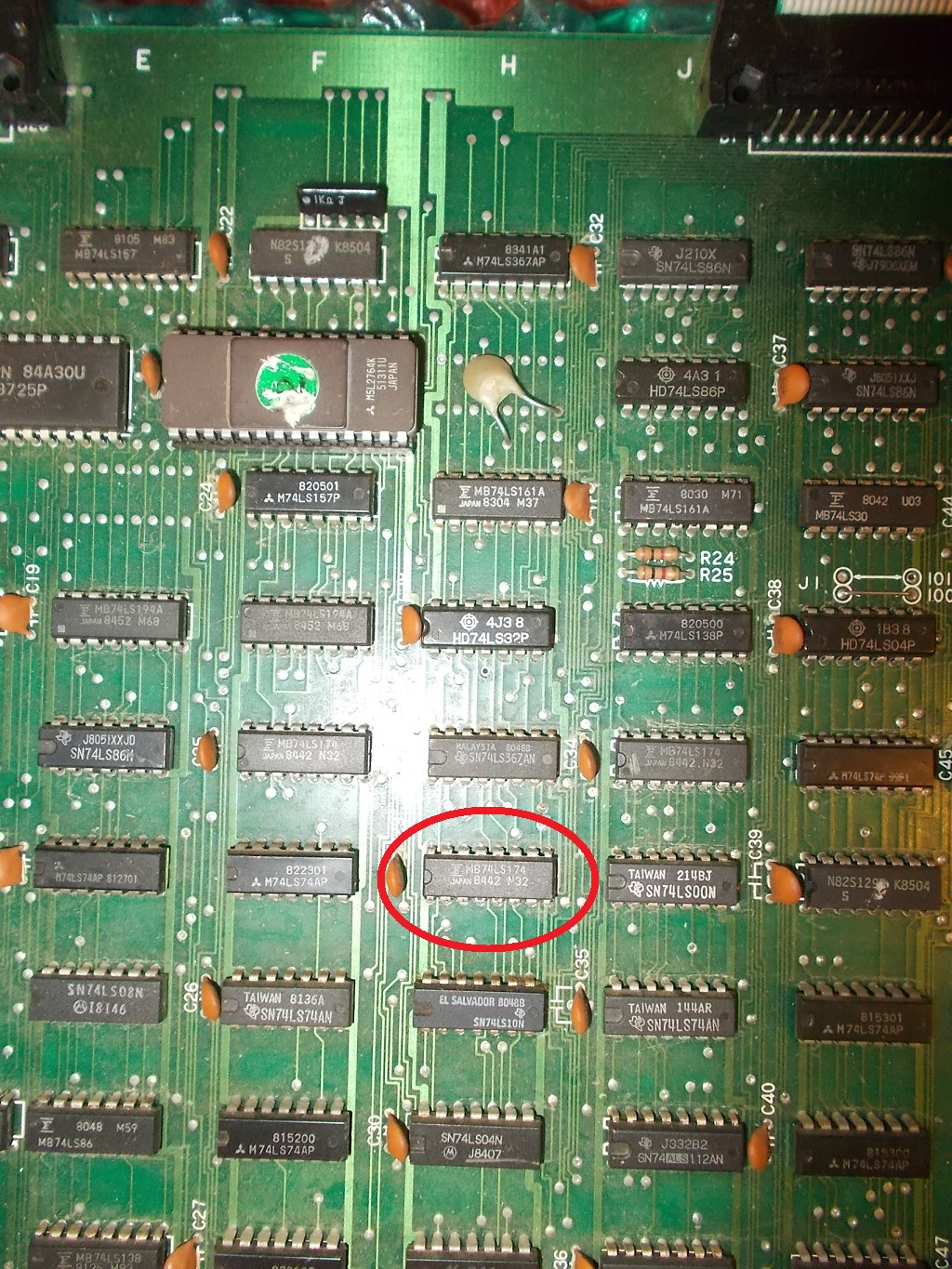
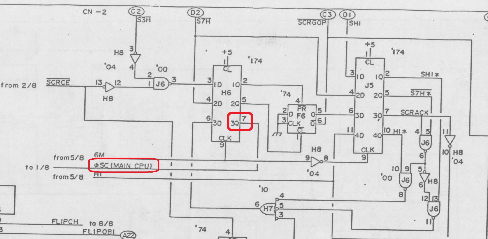
With the help of schematics I traced the clock input back to pin 7 of a 74LS174 @H6 located on CPU board, chip was again from Fujitsu :

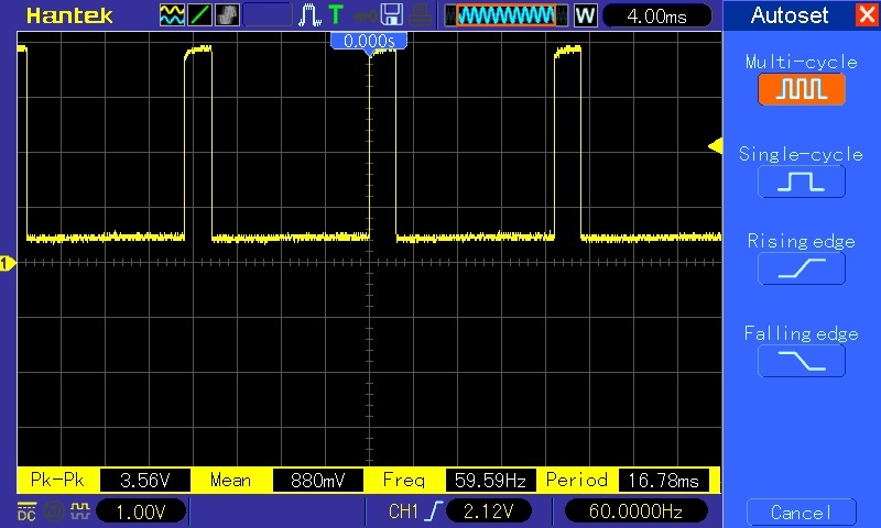
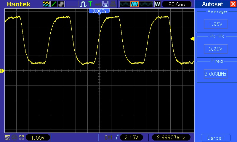
Input pin 6 was correctly receiving a 3 MHz signal:

I made piggybacking with a good known IC and board succesfully booted into game:

Chip obviously failed the out-of-circuit testing:

Replacing it fixed board completely.Double repair job done.

 Posted by at 11:08 pm
Jun 082019
 

I got this Bombjack Bootleg board a while back when I just couldn’t find any original boards for my cab. I since got an original board for it but this bootleg has been left for repair since then.

It was sold as “graphic & sound issues” without more explanations. Lucky though, these bootlegs are identical to the original boards.

A first visual inspection reveals a few loose & broken filter capacitors and a couple of messy traces near the edge connectors. Hard to say without a magnifier if they’re broken. The caps won’t be an issue for now so let’s focus on the traces


I could do a quick continuity test but as it happens, somebody sent me one of those cheap chinese microscope things. They’re essentially a USB webcam , so this is a good opportunity to give it a test.

Indeed two traces were broken, a quick solder bridge will fix that. Handy little toy that thing!

Next, I had to make an adapter since the board didn’t come with one.

On these boards the video signal comes from a separate connector on the far edge of the board. You can already spot there’s an IC missing there too

This might explain the graphic issue.

But first let’s finally power the board and check what we get.

So our colors are off, some graphic information is missing. There’s no sound coming from the board either. The wavy effect on top of the screen is an artifact of my monitor being in need of a re-cap so we can ignore this.
Let’s first take care of that missing IC. Looking at a photo found online, this should be an LS174 flip-flop.

I then checked the schematics and this confirms it as a pair of these is handling the color signals. Our missing IC at 8B handles the blue and part of the green signal.

Let’s drop a fresh one and see if this restores our picture.

Success!!
Now to address the sound issue. Probing my way from the amp back I eventually realized I’was not getting any signal. All outputs on the sound ICs (three AY-3-8910) were dead , I suspected the z80 controlling these.

Swapping it with a new working one restored the sound completely board … here’s a photo for proof :

In addition to this I did make a couple of mistake on my adapter, meaning the controls worked incorrectly. I spent some time trying to troubleshoot this till I double checked my adapter. ah well.  Another case where having another working set would prove useful.
Anyway the board is working fine now, but while I tidied a few loose capacitors around the board I spotted this unpopulated section of the bootleg board:

Silk screen and holes for two leds and resistors. Comparing to an original board and checking the schematics, these should be indicators for the 5v and 12v lines.

While this is not strictly needed it’s an easy thing to just add them . I went for a green 5V and red for 12V

yay . a fully working Bomb Jack bootleg.
And for those preferring the video format:

Namco System 1 ROM boards repair log and ‘CUS95’ reproduction

 PCB Repair Logs, Reproductions  Comments Off on Namco System 1 ROM boards repair log and ‘CUS95’ reproduction
Jun 072019
 

Recently I received a pile of faulty Namco System 1 hardware.I’ve been sent boards grouped by type because, as you may know, it’s a complex system made of a smaller CPU board and a bigger ROM board.I started to troubleshoot the latter.Three of them were tagged as “working but with sound issue” when tested with the same Pac-Mania ROM set :

The issues went from corrupted sound to lack of some music tracks :

Using an audio probe I figured out the sound was properly coming out the YM3012 DAC but then got corrupted before being amplified.In the middle there are two TL084 quad OP-AMPs :

This part is well known to be very prone to failure especially the ones made by Texas Instruments manufacturer like in this case so I removed them all and they failed the out-of-circuit testing :

Replacing them with good ones restored full sound but while I was testing the boards I noticed some inputs were not working on one.A quick visual inspection revealed this :

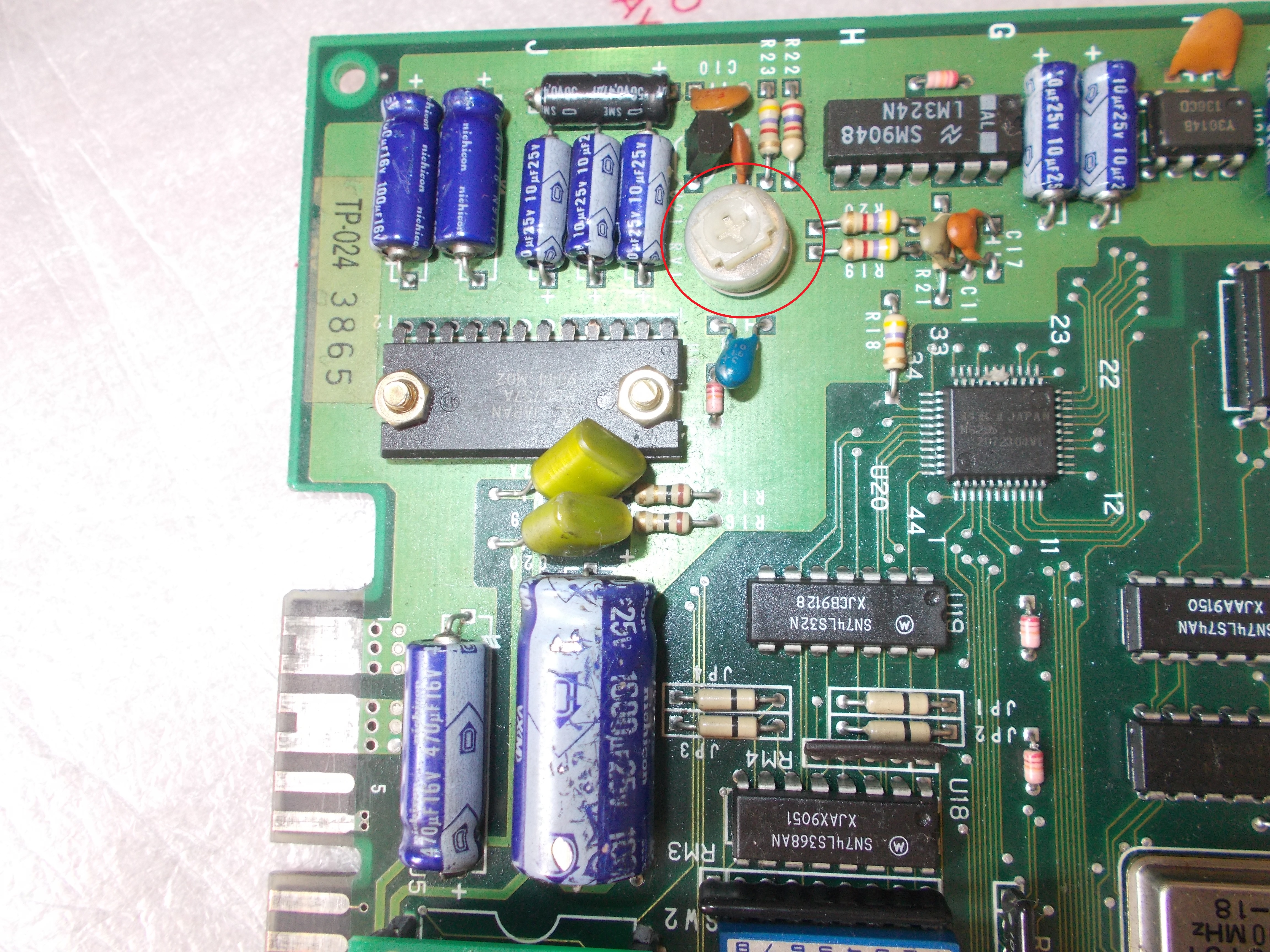
The custom resistors/capacitors array marked ‘CUS95’ was cracked in half.Not having a spare I decided to analyze the part and reproduce it :

Three boards were fully functional now.The last one had also other issues besides sound not properly working as most of graphics were missing replaced by garbage,  sprites were barely visible :

The tilemap generation is handled by the custom ASIC ‘CUS123’ (plus the ‘CUS133’ on CPU board) which generates the addresses to the character ROMs:

It was most likely faulty so I replaced it :

This restored the graphics and left me with the sound issue to fix, music were completely missing on this board:

Replacing the two TL084 OP-AMPs didn’t do the trick this time so I went to probe the rest of circuit.I found that the 78L06 voltage regulator that provides +6 Volt to the YM3012 was outputting only +2.7 Volt :

Replacing it restored full sound.Namco System 1 multiple repair accomplished.


 Posted by at 11:27 pm

Sheriff (conversion) repair log

 PCB Repair Logs  Comments Off on Sheriff (conversion) repair log
Jun 072019
 

Had this guy on the bench for far too long now. The reason? Its a horrible mess of wires used to convert it from something else. Not sure if this was some kind of factory conversion or someone was churning these out at one point in history but its not really something I want to work on again.

So, on power up I get this

When I first saw this on the video I was sent my first thought was one or more 161 counters had gone bad and then I started looking at the schematics (for Bandido) I found what I hoping to find.

There are actually 4 of these (the other one is on the previous page) so I was half prepared for when the PCB arrived.
When I tested the PCB for myself I could make the issue slightly better with more voltage but never managed to get it perfect within the upper voltage limits.

First thing I noticed on arrival was although the schematics were accurate the chip locations were not.
Like I said at the start of this the PCB is a mess of wires which are directly soldered to other parts of the PCB’s which made taking this stack apart a little tricky but needs must so I did.
Finding a bank of four 161 counters was easy enough.

Feeling sure of my diagnosis I removed all four counters and tested them out of circuit but they all passed.
I socketed and replaced them anyway as I know from previous experience these are a fail point.
When I retested the game the graphics issue was now fixed! I could even lower the voltage to 4.8 without problems. I guess these old ones had started to fail and gone out of spec.

Next issue was the sound but before looking into that I was very curious about the intermediate PCB half hidden under the sound board.

This thing is a horrible freak of nature.
I knew it was something to do with the controls but why so much circuitry? What is that EPROM looking chip on there? and why did it look homemade?
Sadly I don’t know the answer to that last question but I have a fair idea of what the other two are.

First up that EPROM looking thing.
I desoldered it and tried to identify what it was. Best picture I could get from the scratched off markings were this

I could see it was likely a Toshiba device and it had “333P” appended so after a fair amount of sleuthing It was deduced that it was TMM333P device.
As I had no way of reading this with any of my programmers I resorted to using the faithful Arduino to dump its contents. After successful extraction it actually identified in MAME as a ROM from Jatre Specter. This made little sense until I traced out the connections and realised it was actually hardwired to address $4E7 so one ever gave out the byte 0x3A. Furthermore only 5 bits of the byte were being used and they are only used to permenantly enable the adjacent logic chips.
My best guess here is the bulk of this PCB is for obfuscation purposes.
On another sidenote, I tried making a small replacement PCB for this using a CPLD and while it worked as expected without the outputs connected it went wrong when they were connected up. Looking on the scope I could see a fair bit of bus contention so I think the CPLD was just too fast for this old hardware.
Anyway, on with the repair.

There was no sound. I started probing around the 8035 and found it was giving out garbage. I pulled the 2708 ROM and found that also full of garbage. I did try erasing it and reprogramming but it wouldn’t program at all. I replaced this with a slightly modified 2732 EPROM.
I ordered a new 8035 and while waiting I decided the best course of action would be to refurb this whole PCB as much as I could. All capacitors were replaced and replaced some of the logic IC’s too just for good measure.
Found a few dodgy looking solder joints like this one along the way

The replacement 8035 came from eBay but it was DOA. The seller send me another no questions asked and this one worked fine.
That’s about it for this one.

Worth noting with this conversion that it was been wired to use the player 2 joystick as the aiming function for player 1.

 Posted by at 7:45 pm

Nemesis (Konami GT conversion) repair log

 PCB Repair Logs  Comments Off on Nemesis (Konami GT conversion) repair log
May 252019
 

Received from Portugal a faulty Nemesis PCB for repair, actually a conversion from Konami GT on GX400 hardware.Set is made of a CPU board :

And a VIDEO board :

The game was full playbale with sound but the graphics were glitched as there were jail bars all over the screen:

The fault was obviously located on the bottom VIDEO board therefore first of all I ruled out all the custom ICs by swapping them in a good board, they were all OK.Then I focused on a couple of rows of 4164 dynamic RAMs (some were already replaced) :

They are 64K x 1-bit devices, here’s pinout :

On this board they are used as sprite line buffer like schematics show :

I went to probe them with my scope and I found one with an unhealthy signal on data output pin (good signal for comparison on left of below picture)  :

It was the chip @5H which I prompty removed and replaced with a good one :

This fixed the issue and board competely.Repair accomplished.

 Posted by at 10:55 pm