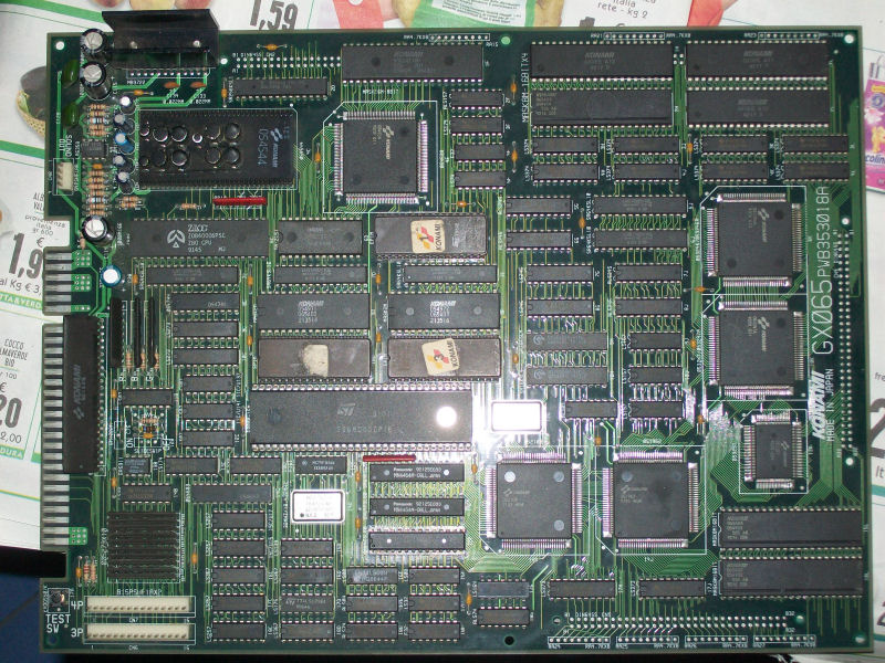
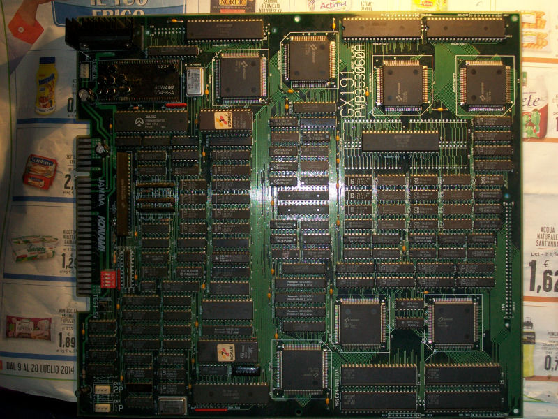
Got today in the mail this mint original Konami X-Men PCB bought as faulty:
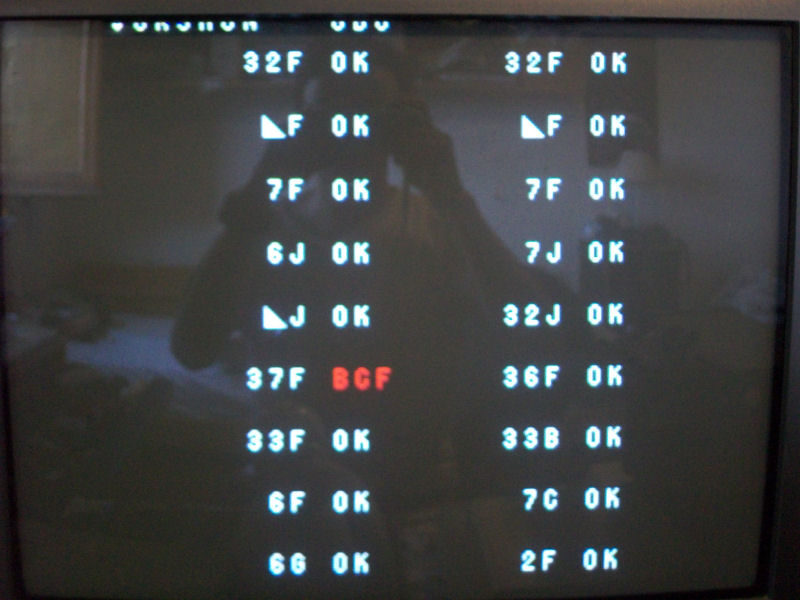
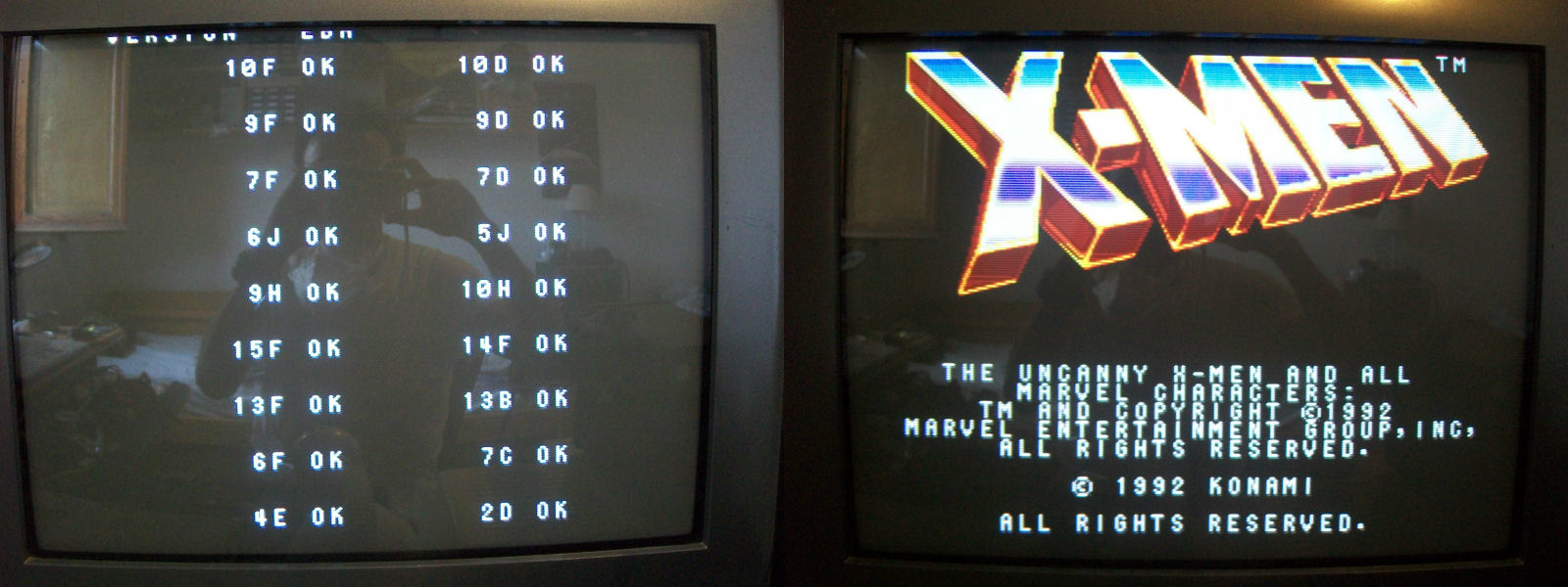
Once fired up I got this:
So, RAM/ROM test reported a bad IC @37F but this was not the real location of the IC since there was no location 37F on PCB.So, clearly there was some trouble in the tilemap generation, this was confirmed by the word “BAD” which became “BCF”.So, I launched MAME:
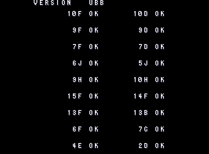
and, comparing the emulator and real PCB test results screens, I could identify that the faulty IC reported by test was the Panasonic MN4464 (6264 compatible) SRAM @ 15F
This confirmed my theory about bad generation of tilemaps since this SRAM is used by the near ‘052109’ ASIC (tilemap generator).
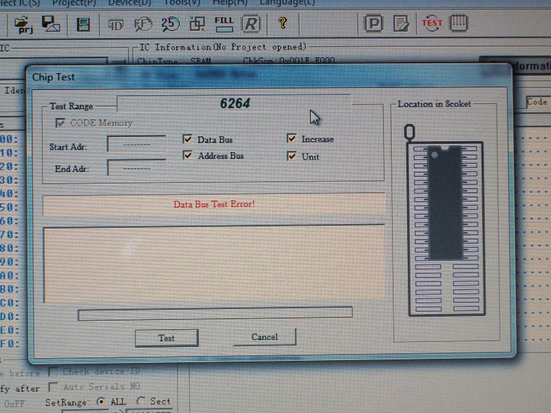
So, time to desolder the IC and test it out of circuit corfirmed the RAM as bad:
Fitted a socket and a spare 6264 SRAM and I could add also this cool game to my growing collection!
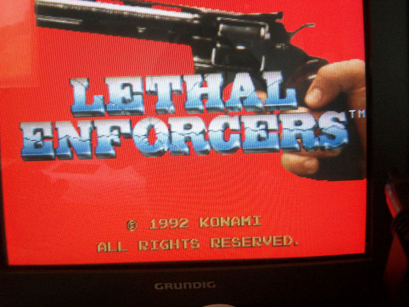
This is the second Lethal Enforcers PCB I fixed and also in this case it has been a pretty easy repair .
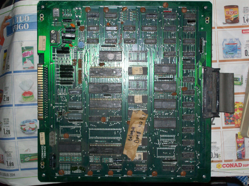
Board was mint and clean:
When powered up it I got this screen:
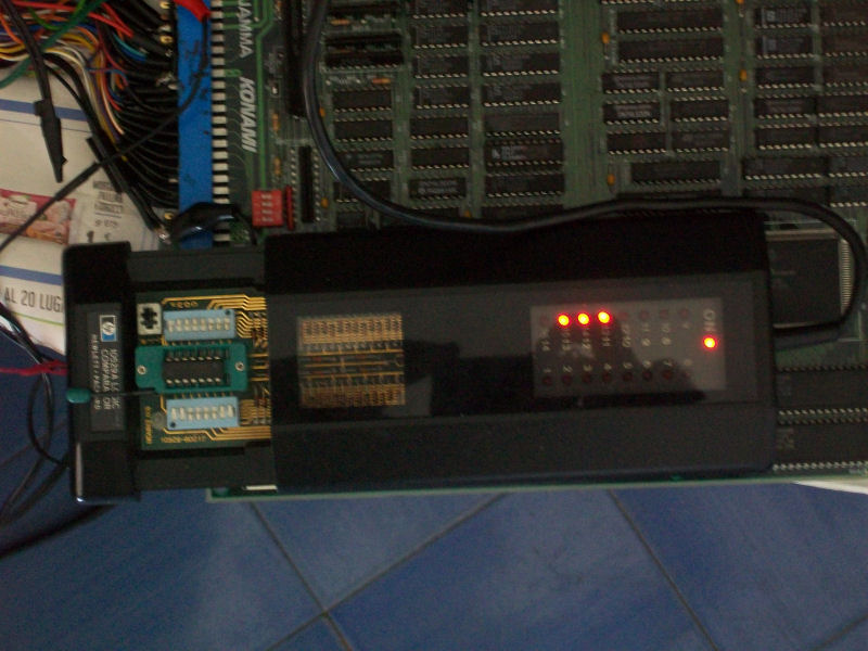
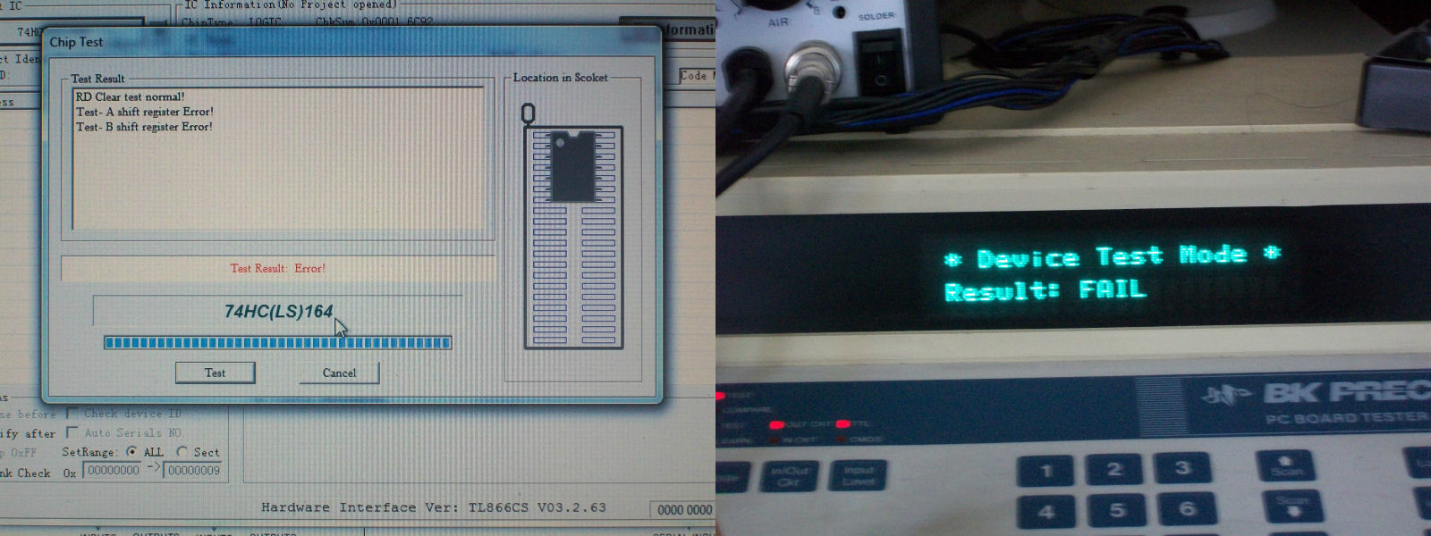
Screen was static but from the clicking sound I understood that watchdog was active so, for first, I disabled it by closing jumper ‘JP’ near JAMMA edge.In this kind of Konami hardware (like in many others) RESET is generated by pin 10 of the SIL custom ‘051550’.Probing this revealed that signal was good (first LOW and then HIGH) while RESET line (pin 37) of the main CPU HD63C09EP was stuck LOW.I traced it back to a 74LS367 @N6 which output was good and input of this to an output (pin 13) of 74LS164 @H3.Tested this with HP10529A logic comparator revelead bad outputs (pin 11, 12, 13).
So I desoldered and tested it in my EPROM programmer and B&K Precision 560A IC tester which confirmed it as bad:
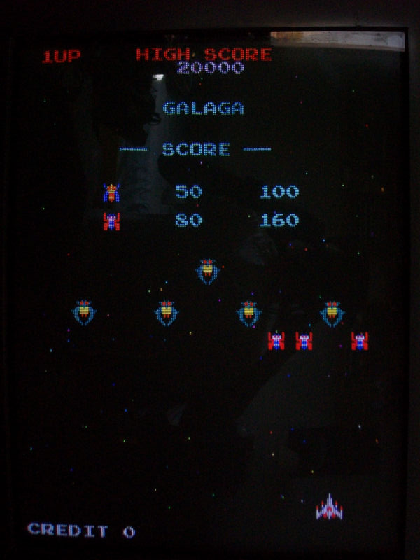
Stored this original Galaga PCB from a while but never looked at it deeply:
It had a piece of tape on it saying “Dead” but at a first visual inspection I noticed it missed the custom marked ‘0020’ (tilemap address generator with scrolling capability) on CPU board @1H.So I thought game is over, I was doomed .The only chance I had was using some modern replacement (based on CPLD or FPGA).But, then, my savior appeared under the name of Silvio, a guy met over over ArcadeItalia forums (thank you again and again..) who very kindly donate me this custom chip.
So, time to build the needed JAMMA adaptor and I fired up the board getting this:
Horizontal white stripes all over the screen, a good point to begin from 🙂
So, I started to touch and press the board in different places and I noticed that if I pressed the custom marked ‘0200’ (GFX data shifter and mixer) @4H on video PCB , issue disappeared.So, it was clearly a matter of bad contact due a corroded socket and this was confirmed by replacing it with a new one:
I was happy since I thought board was 100% fixed but when I started a game I noticed (or better, heard..) something odd : all sound FX (explosions, etc..) were fine but music was muffled, almost distorted.
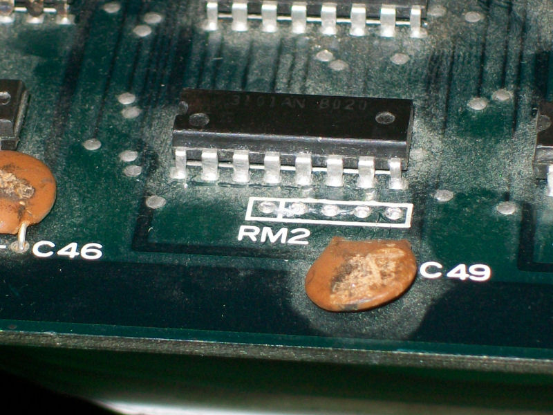
So , schematics in hand, I was starting my troubleshooting on audio section when I noticed that a 1KOhm 5 pin resistor network @RM2 was missing from my board:
Looking at schematics I found that this should have been connected (and acted as pull-up) to outputs of the near N3101AN (7489 equivalent) @2A which is one of the two RAM used in sound circuitry .So, with confidence I installed a new resistor network and…. music really came back crystal clear as it should be.
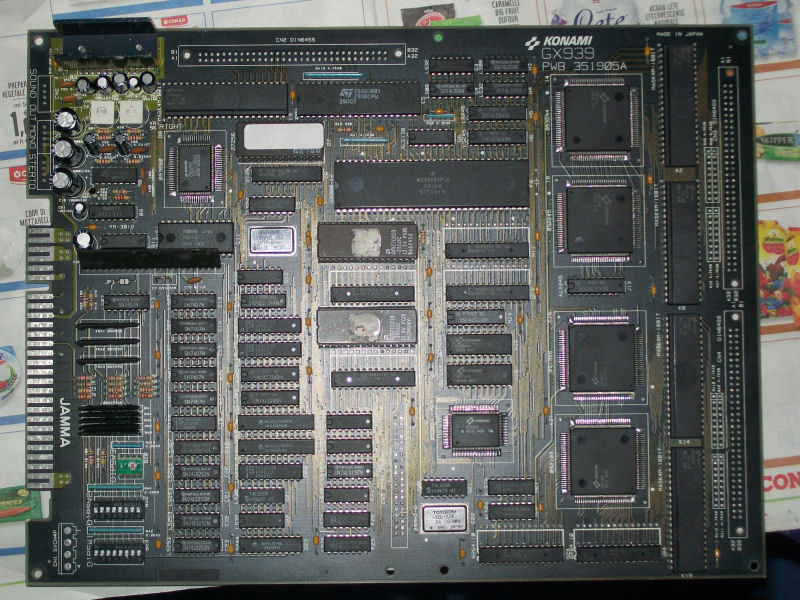
Received today from Spain this Lightning Fighters orginal Konami PCB (bought on Ebay some days ago):
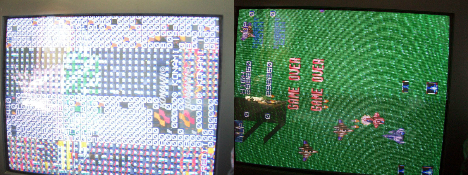
Seller sold this as faulty saying game suffered from graphics glitches.
He was right (positive feedback for his honesty…)
I immediately thought it was something related to tilemap generation since part of screen was doubled and drawn in wrong place while sprites were good.So, I started to check this part of circuit.This hardware, like many other from Konami, use some ASICs in QFP package to generate parts of graphics.This PCB uses two of them to create the tilemaps, they are marked ‘052109’ and ‘051962’ and always used in pair.Checking them I found a couple of lifted pins on the one marked ‘052109’, I reflowed them but issue was still present.
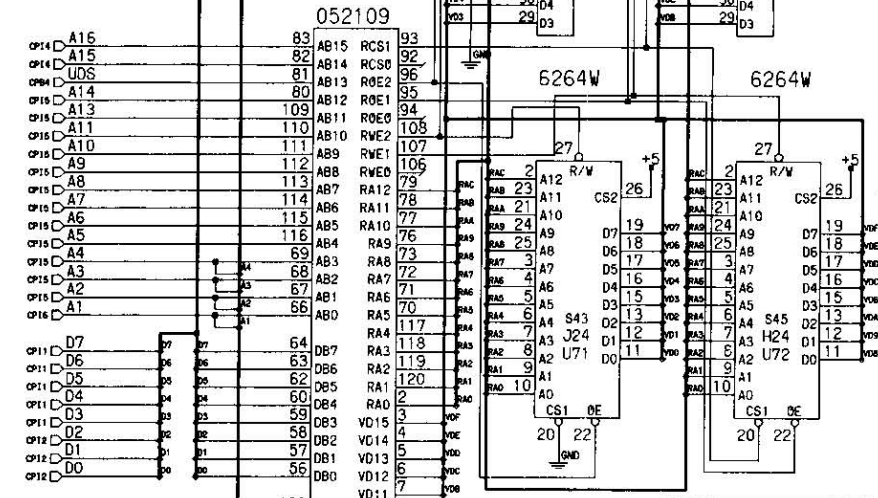
So I started to think about : technically speaking, an ASIC behaviours like a CPU, so in this case it takes datas from graphics ROMs and stores them in RAMs.When it wants to read these stored datas, it addresses the RAMs.
So my issue should have been due a bad RAM adressing since screen fullfilled of zeros, graphics drawn in wrong place are clear symptoms of it.So, I started to check the two 6264 SRAM @H24 and J24.All address lines was shared between except for A2 (pin 8).This abnormality was also confirmed by schematics:
I noticed that someone replaced (or desoldered for testing) these two SRAMs previously so probably he managed to cut the track between the two address lines.So I jumpered them with a bit of AWG30 wire and all graphics came back to normality:
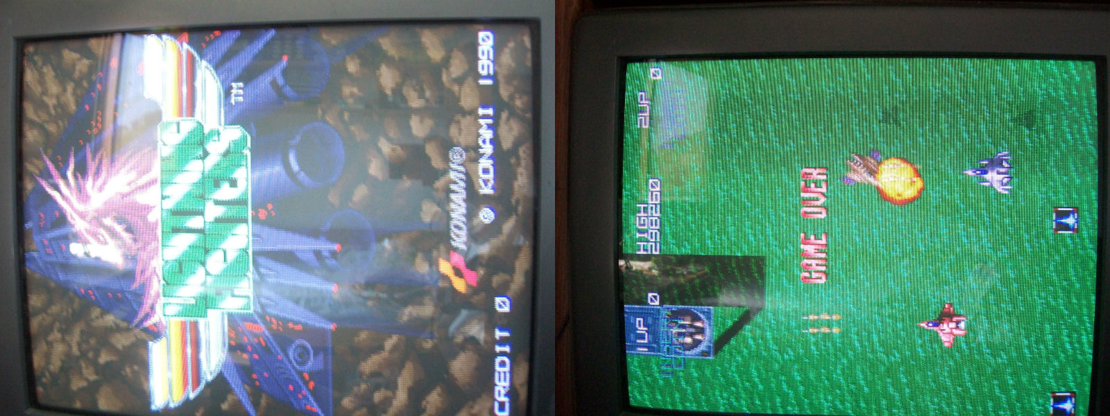
I recently sold this PCB but after a week I was told the board had developed a fault.
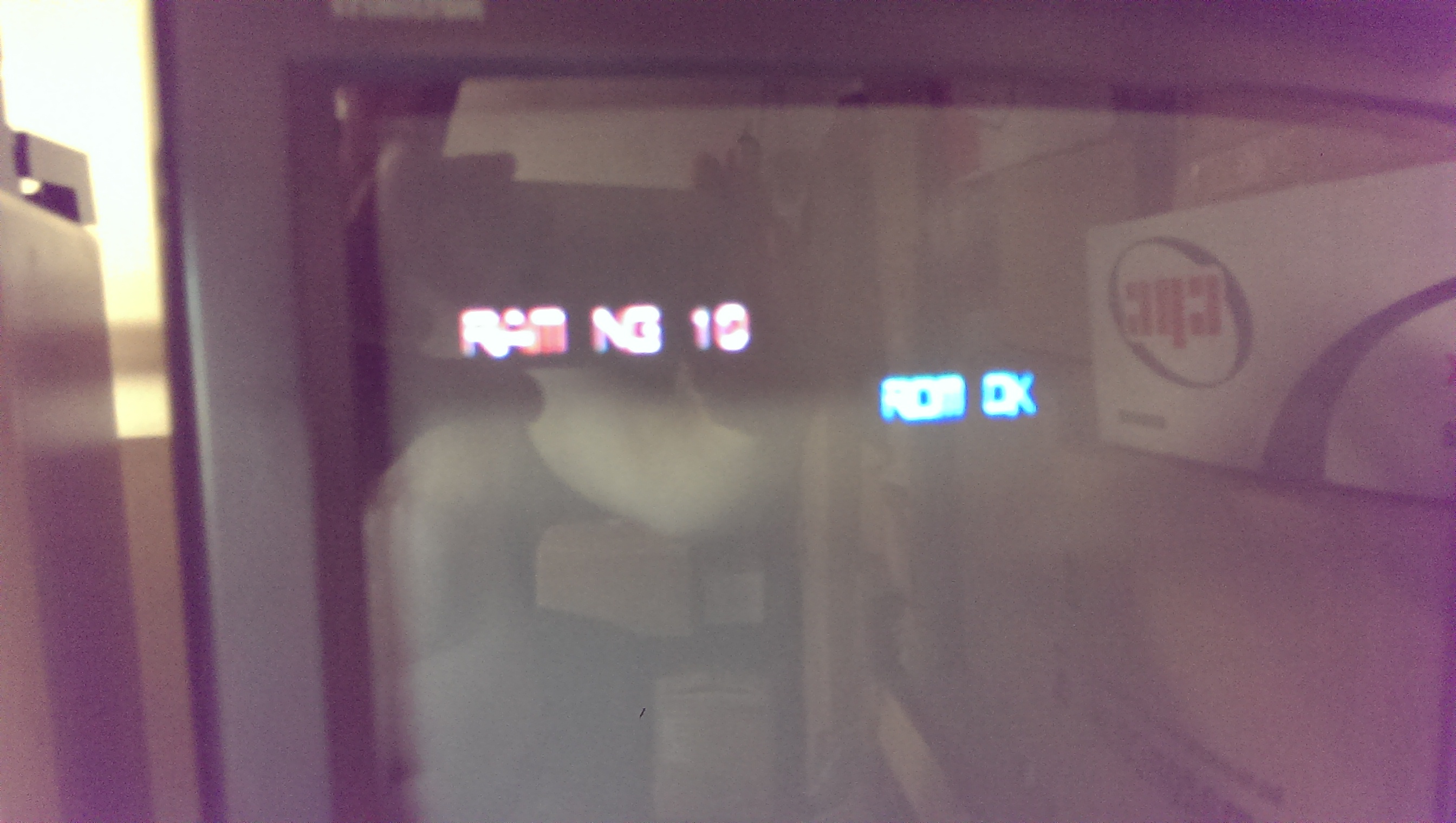
The fault showed up as “RAM NG 10” at boot-up and there was some issues with the sprites.
There is absolutely no logical meaning to the error message so using MAME I started corrupting different RAM values during it POST to see what RAM errors were flagged up during which memory writes.
Originally I couldn’t understand how the awful V30 CPU worked. Without knowing how it worked I was unable to use the MAME debugger effectively. Charles MacDonald came to my rescue and told me how the V30 addresses were set. Thanks very much to Charles.
You can see the outcome of that exercise in THIS previous post.
So now I knew for sure that the fault was with the sprite RAM. Now the next challenge, which RAM chip is the sprite RAM?
I originally tried shorting some address/data lines on RAM chips to see if any other errors were flagged but strangely it didn’t show anything else at all.
With nothing left to try I started making my own schematics up in the hope I could work out which RAM was responsible for the sprites.
Due to the complex nature of this board set, I was stuck for quite some time looking on the lower video PCB assuming (yes I know) that this is where the sprite RAM could be but was unable to find any problems at all.
Taking a step back I reversed the PAL chip XM_A-7D- into equations. Using these equations and the schematics I had drawn up I could take an educated guess as to what RAM chip was the sprite RAM.
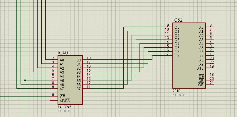
Knowing that the sprite RAM lies at address 0xc0000, this means that address pins A19 & A18 would need to be active. Looking at the equations I could see that output pin 17 of the PAL chip would fit this address so I followed the signal which led to the /CE line of a 74LS245 of IC40 on the top CPU PCB.
The only chip that this chip goes to is a 2018 RAM chip at location IC52.
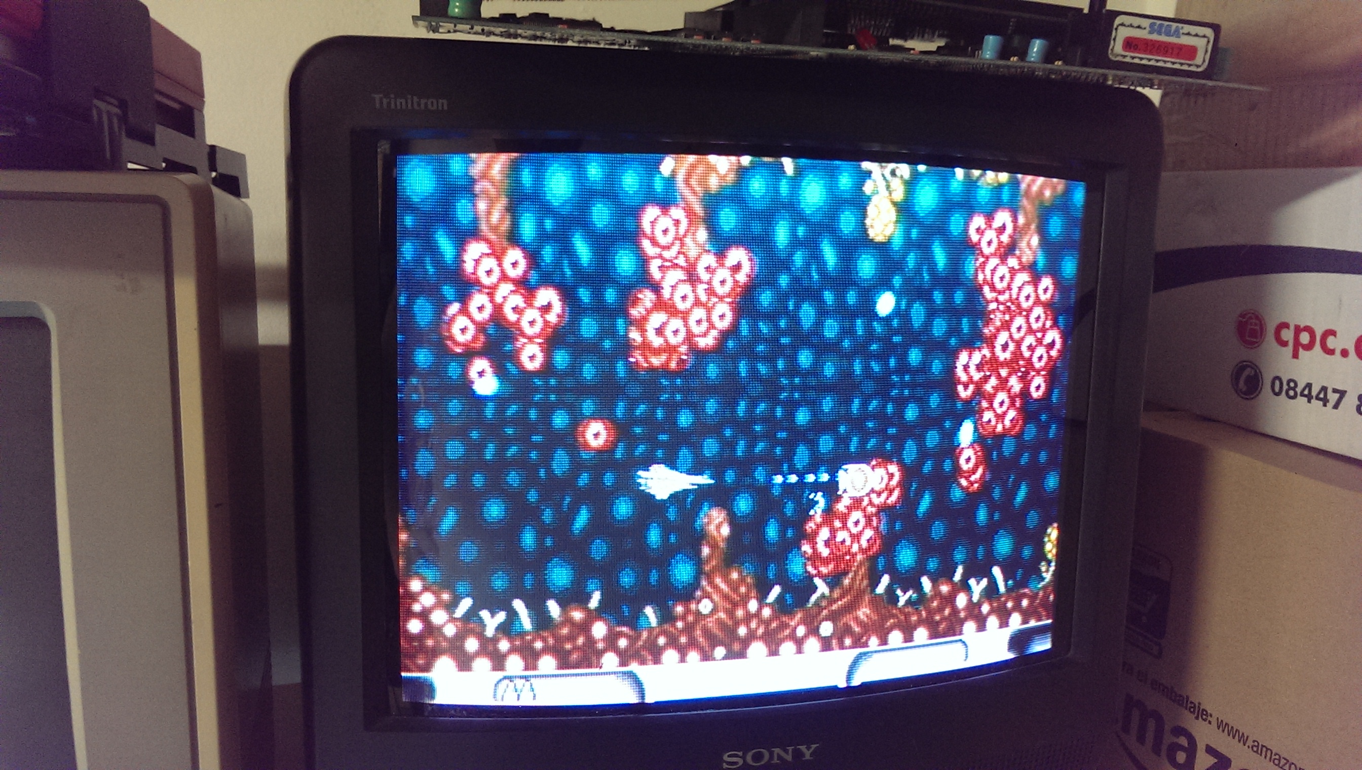
This was pretty good news. I removed the chip and it failed the tests so I replaced it and now all the POST tests pass.
The sprites are all back to how they should be too.
Ill be keeping hold of this board I think. It was one of the first games I ever bought since getting into this hobby so it will stay with me for good now.