Porchy

Jul 222019
 

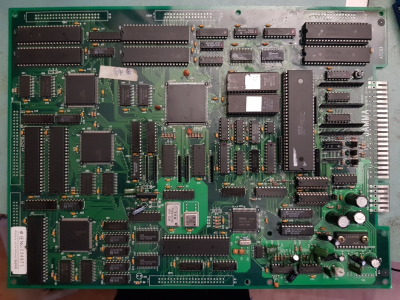
One drunken day at the excellent Revival event I offered to look at a Nintendo Space Firebird PCB.
Initially I was given the eBay link which had a few pictures of the fault.
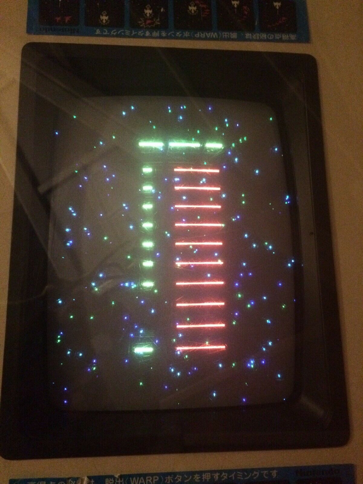
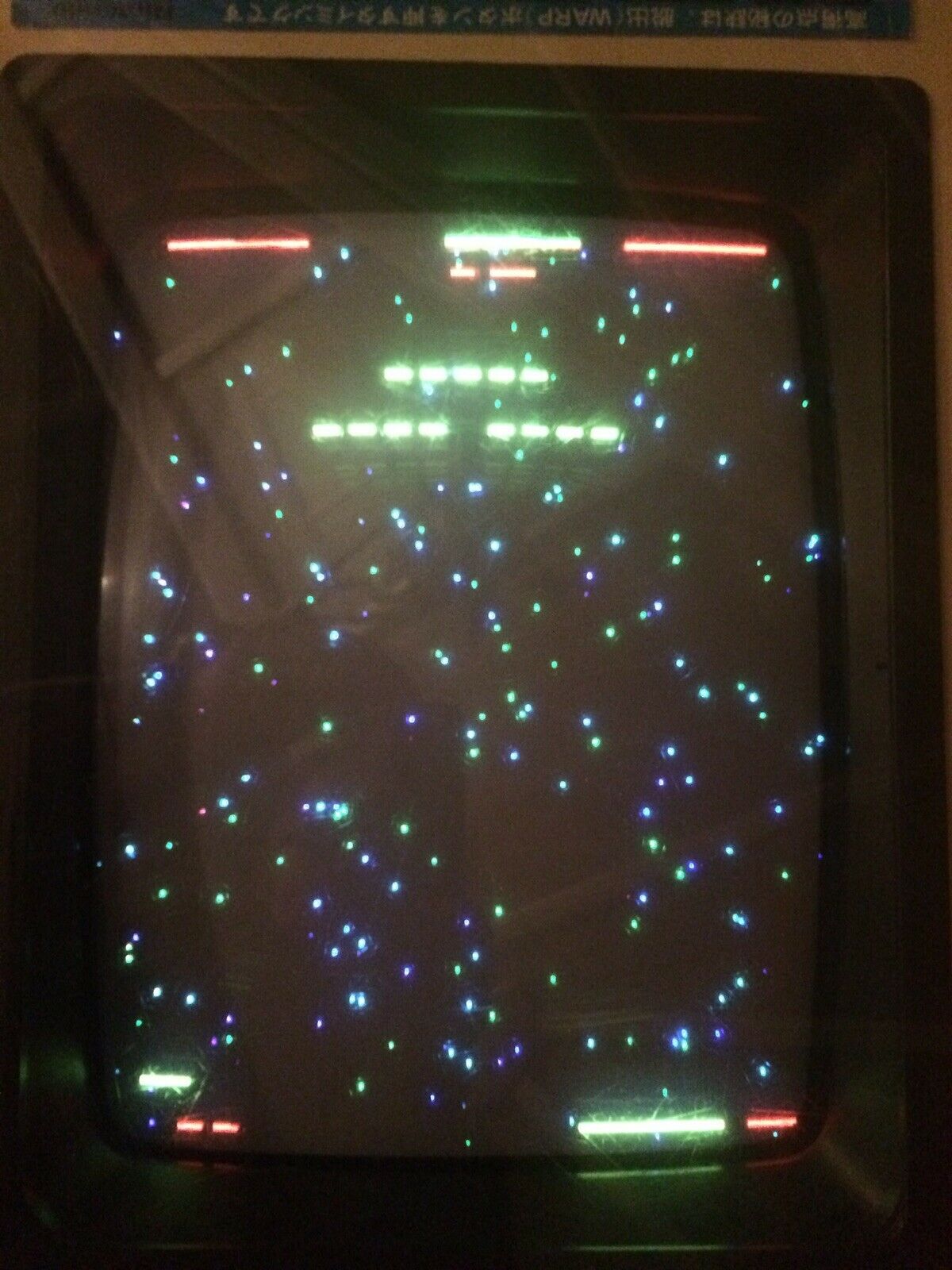
When I got the board I did my usual visual checks and found a few things I didn’t like the look of.
First up both main RAM chips are socketed. I removed these to check out of circuit and found this
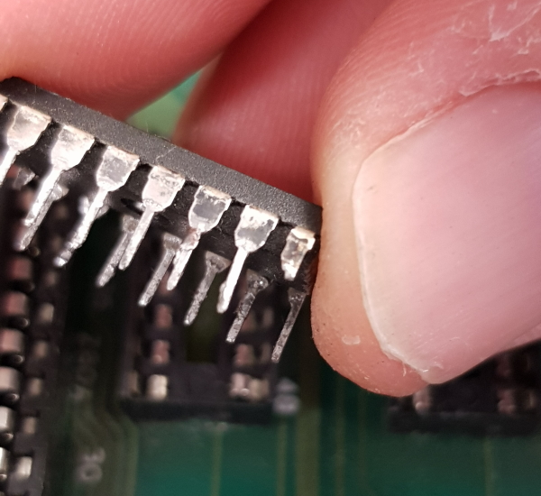
I fixed that up by removing a leg from a donor chip and soldering it on
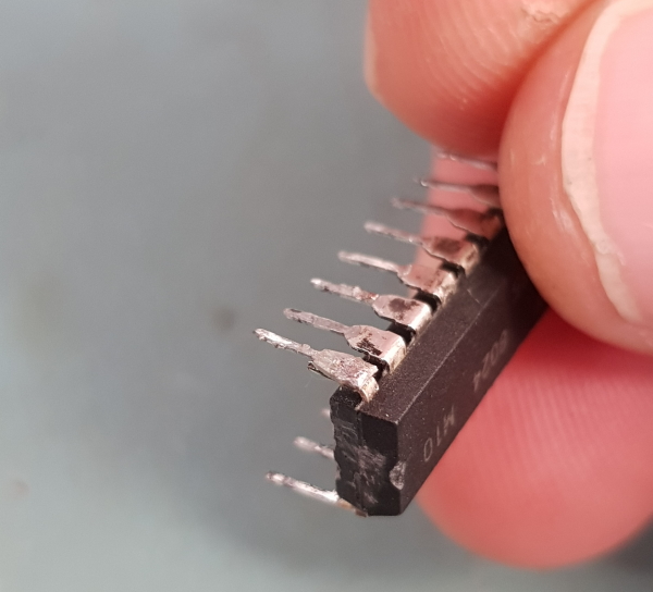
Next up was the 8212 Input/Output port. It too was socketed with a single wipe socket but what really got me suspicious was the state of the soldering
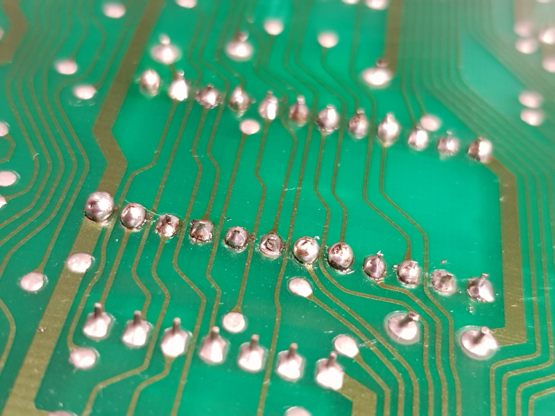
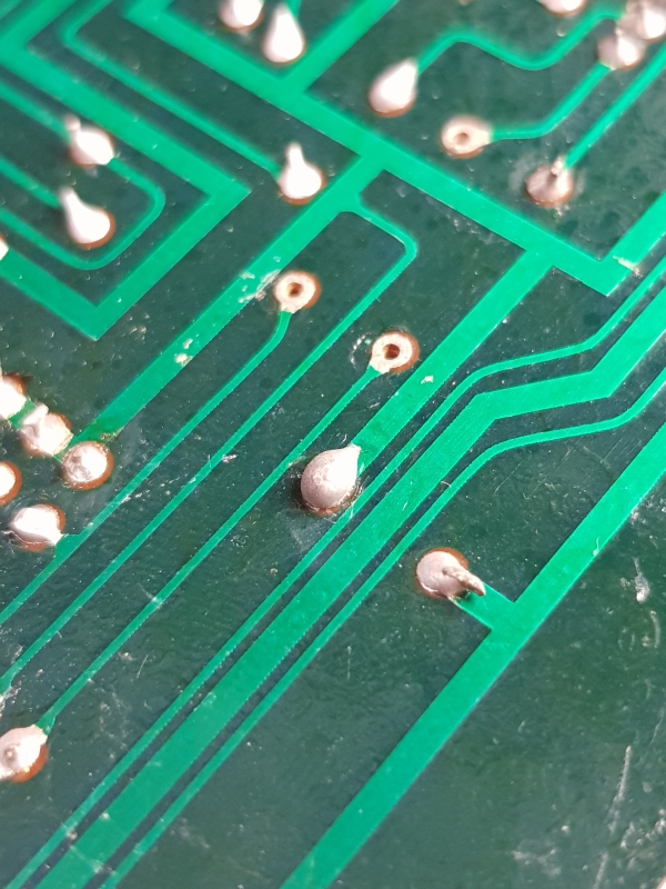
I wasn’t a fan of this so desoldered it. When I desoldered it I found this
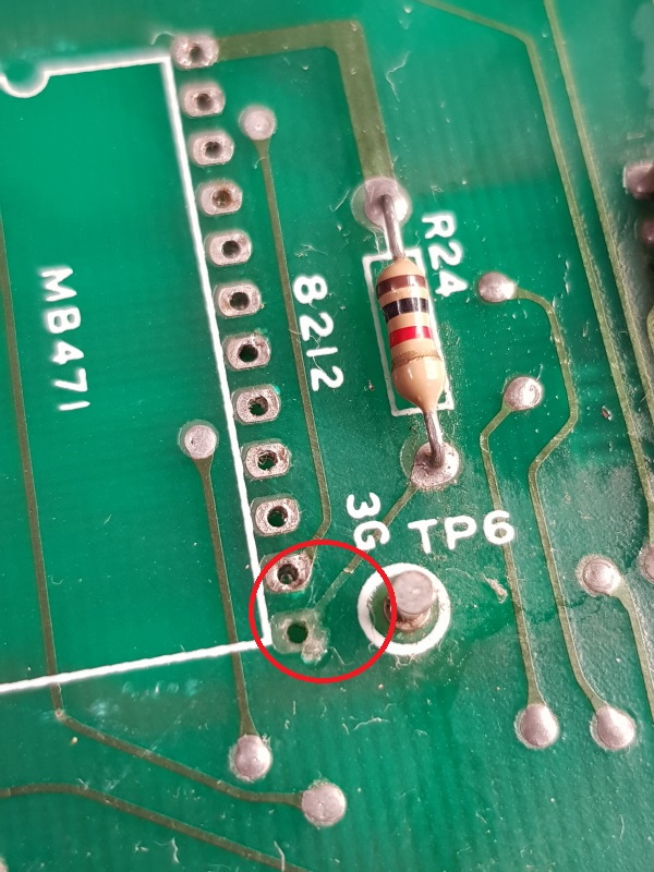
A bit of trace has been lifted there. I can only assume this has been removed before.
I fitted a new socket and moved on.

Found a burnt looking resistor on the sound PCB
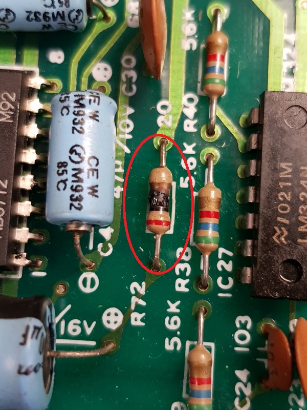
The resistor still reads 20 ohms but i will replace that once my parts order comes in.

Lastly there were a few areas with the solder mask removed and solder on it. Not a huge problem but it needs addressed.
I cleared the excess solder from these places and covered them using a Chemtronics pen.
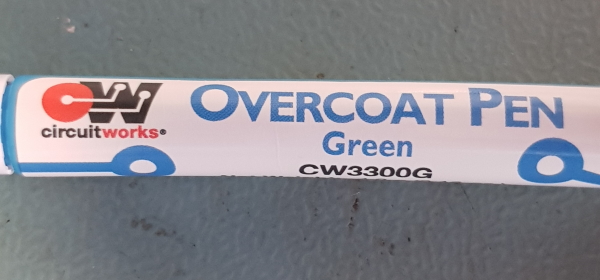
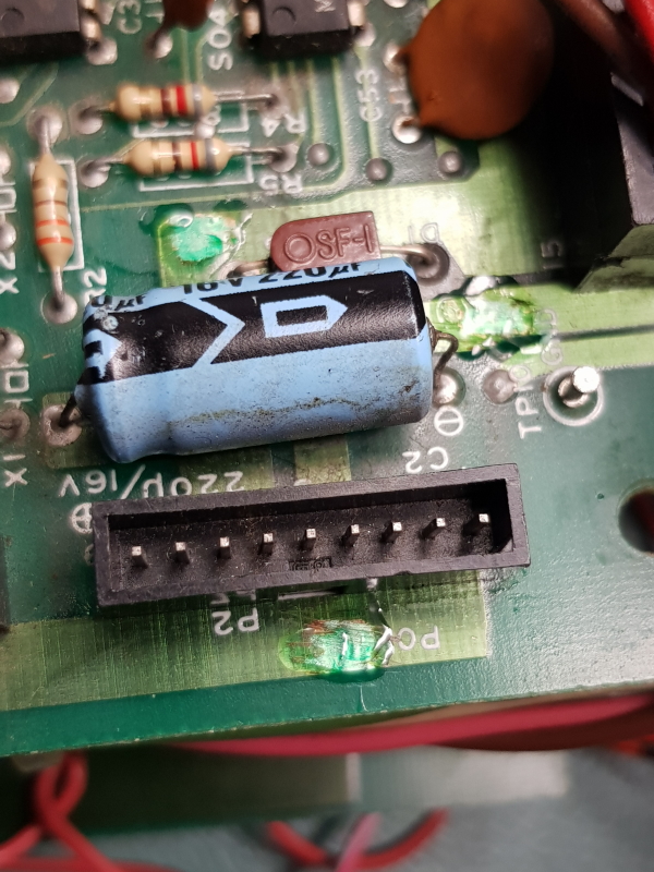
Not pretty but it does the job.

Firing up the PCB for the first time confirmed the original fault was still present.
As the fault was with the video I looked there first.
I started by reseating the two socketed RAM chips
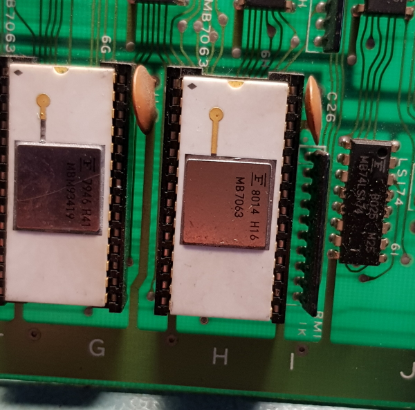
To my surprise this fixed up the graphics. Not sure what effects the previous fixes would have had but Im not removing them to find out.

New problem now. The game hangs at the title screen at the same point every time.
Whenever I get issues like this I always think RAM or ROM issues.
I had already confirmed the RAM so went on to dealing with the ROM’s.
All of them were a match for Space Firebird according to MAME’s ROMident but the ROM at location 5J was for a different version of the game.

It should have been this

I erased and reprogrammed the 2716 EPROM and now the game plays fine.

While comparing gameplay against MAME I realised some colours were missing
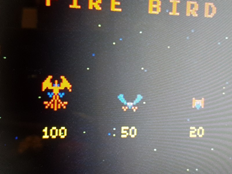
This should look more like this
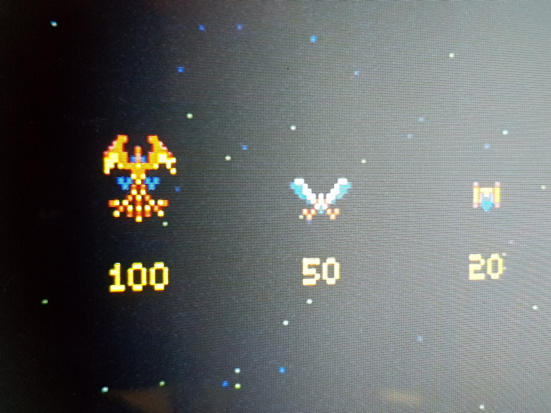
I chased this round for quite a long time only to realise that the 74LS04 inverter I was using (as stated in the manual) to invert the colours was my problem. Switching to the proper Nintendo inverter PCB made everything look right again.

All that’s left now if to replace all those capacitors on the sound PCB and that burnt looking resistor and this board is done

 Posted by at 6:18 pm
Jul 072019
 

Today I’ve uploaded the latest version on my BINman software to v4.5.0
The main addition here is the inclusion of Fluke 9010 signatures to the checksum area.
Not only does it have support for the 8 bit signatures it also supports the 16 bit signatures.
For 16 bit signatures, it will only support single files so if your hardware has the files across 2 EPROM’s then these will need interleaved or whatever is required to merge them.

Enjoy

 Posted by at 8:04 am

ESP Ra.De. repair log #2

 PCB Repair Logs  Comments Off on ESP Ra.De. repair log #2
Jul 052019
 

Received an ESP Ra.De. board for repair for my friend Vic.

This was the video I was sent originally

This PCB had apparently had work done before but all we knew was the big 240 pin custom chip had been reflowed. This always makes me nervous because if it was destroyed somehow then all further attempts of repair would be for nothing unless I had a donor.
Visual check carried out of the board in general revealed nothing bad so hooked it up to the test. As expected we have no sync and the game does not appear to be running either. I confirmed this as the watchdog was kicking in.
Using the scope I probed the sync pin at the JAMMA connector and found a low sync signal of 13khz.
I started tracing the signal back but it went to the big custom chip that I already knew had been worked on, I also confirmed the main clocks and signal to the custom chip.
With no other ideas at this point I decided to tackle the game booting issue. The 68000 CPU was already in a socket so using the Fluke 9010 with a 68000 POD (Thanks Caius for the extended loan of his POD) I could start troubleshooting.
First off a BUS check revealed data bit 2 was tied low. In actual fact data bits 2 and 3 were shorted together.

I started tracing all the point where these data lines go and one by one started isolating them from the circuit. Once again my search led back to this big custom chip.
Reflowing these two pins on the custom cleared the fault.

At this point I took a closer look at this custom and found if I got the light in at the right angle I could see a lot of dried flux underneath.
Over time flux residue will dry out if not properly cleaned and it can go conductive.
I cleaned this and the bus test now passes. The ROM check between 0x0 – 0x7FFFF should be 1BBA which also passed.

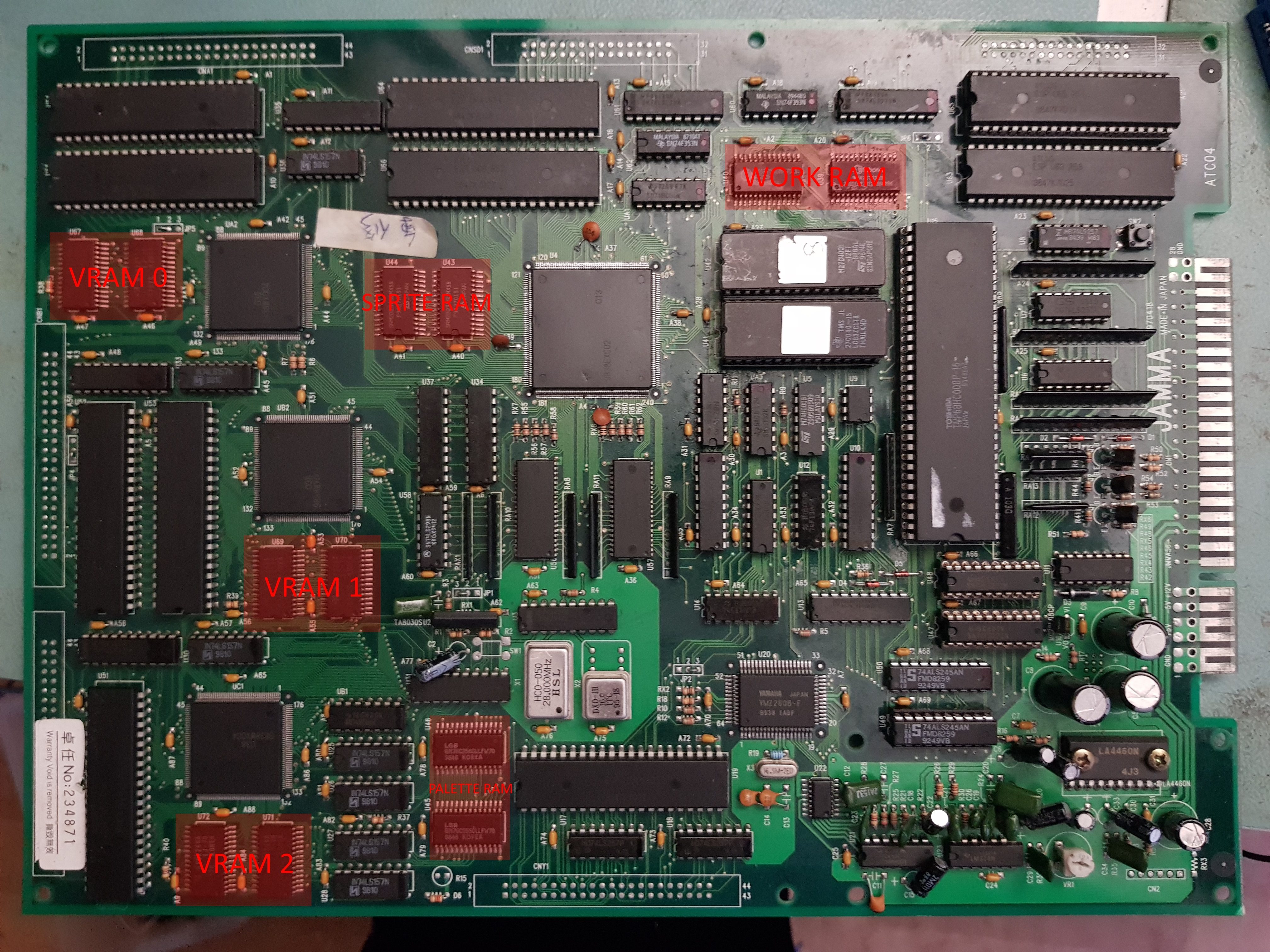
The main RAM lies at location U39 & U40, 0x100000, 0x10FFFF. The Fluke reported a decode error on bit 1 which basically means there is a problem with the address lines.
Doing some manual reads and writes I could see that bit 1 of RAM U39 did not work. I replaced this and retested which then went OK.

I started my way through the rest of the RAM location as per the MAME driver.
The sprite RAM lies at U43 & U44, 0x400000, 0x40FFFF. Once again the fluke reported bits 5 & 6 tied together and once again I was led back to the same custom chip.
From here I just opted to reflow the whole chip. This cleared the issue with the sprite RAM. All other VRAM passed tests.
Retesting the PCB now resulted in a nice looking game for the most part but there was a strange strobing around test and lines that were white. Going into the test mode made this very obvious.
I couldn’t get a good video of this as it all looked fine on a camera.

To began with I thought this was all to do with my test monitor and the sync being a tiny bit high for it but I tested it on all my monitors and cabs and they all gave strange results.
I eventually went back to that custom chip and inspected all the pins again.
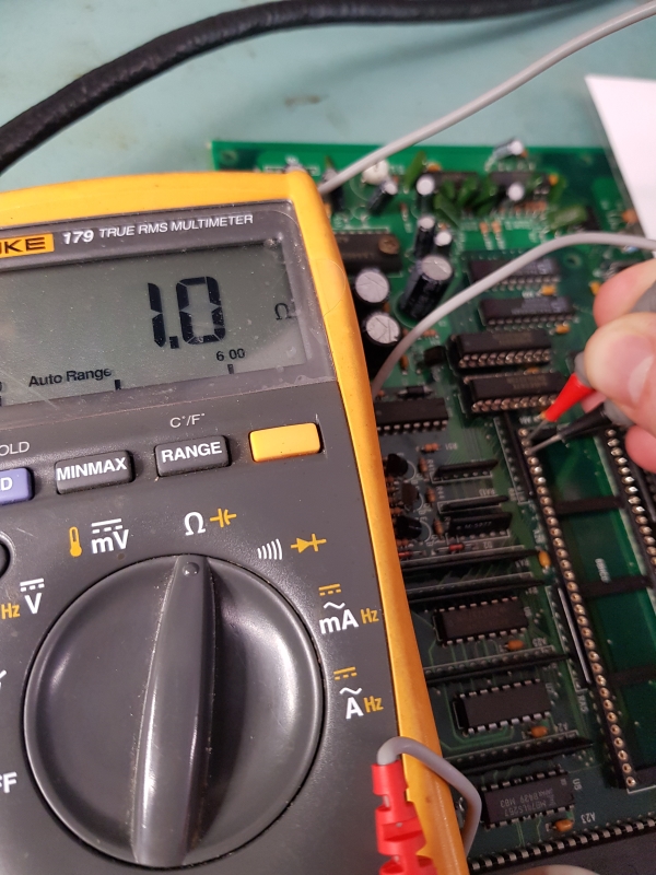
I couldn’t visually see anything but checking continuity on all pins against the adjacent pins revealed a short somewhere around pin 190. A further reflow of these pins resulted in a completed repair

One strange thing about this board is that on boot up it stays in a reset state for around 2 seconds which is the point where the sync reads 13khz. After that the sync steps up to 15.23khz and all OK.

Here is a layout of all the RAM locations on the PCB

 Posted by at 4:38 pm

Sheriff (conversion) repair log

 PCB Repair Logs  Comments Off on Sheriff (conversion) repair log
Jun 072019
 

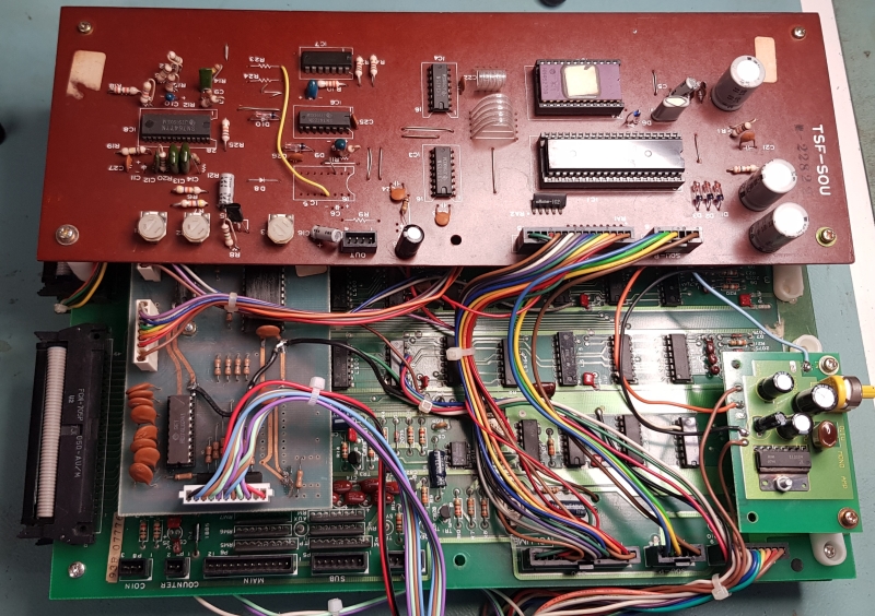
Had this guy on the bench for far too long now. The reason? Its a horrible mess of wires used to convert it from something else. Not sure if this was some kind of factory conversion or someone was churning these out at one point in history but its not really something I want to work on again.

So, on power up I get this

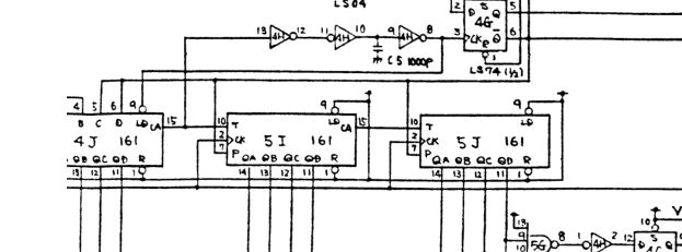
When I first saw this on the video I was sent my first thought was one or more 161 counters had gone bad and then I started looking at the schematics (for Bandido) I found what I hoping to find.

There are actually 4 of these (the other one is on the previous page) so I was half prepared for when the PCB arrived.
When I tested the PCB for myself I could make the issue slightly better with more voltage but never managed to get it perfect within the upper voltage limits.

First thing I noticed on arrival was although the schematics were accurate the chip locations were not.
Like I said at the start of this the PCB is a mess of wires which are directly soldered to other parts of the PCB’s which made taking this stack apart a little tricky but needs must so I did.
Finding a bank of four 161 counters was easy enough.

Feeling sure of my diagnosis I removed all four counters and tested them out of circuit but they all passed.
I socketed and replaced them anyway as I know from previous experience these are a fail point.
When I retested the game the graphics issue was now fixed! I could even lower the voltage to 4.8 without problems. I guess these old ones had started to fail and gone out of spec.

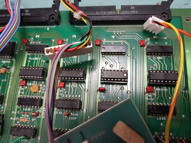
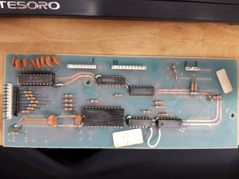
Next issue was the sound but before looking into that I was very curious about the intermediate PCB half hidden under the sound board.

This thing is a horrible freak of nature.
I knew it was something to do with the controls but why so much circuitry? What is that EPROM looking chip on there? and why did it look homemade?
Sadly I don’t know the answer to that last question but I have a fair idea of what the other two are.

First up that EPROM looking thing.
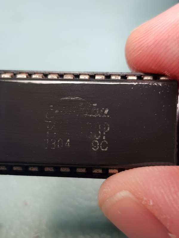
I desoldered it and tried to identify what it was. Best picture I could get from the scratched off markings were this

I could see it was likely a Toshiba device and it had “333P” appended so after a fair amount of sleuthing It was deduced that it was TMM333P device.
As I had no way of reading this with any of my programmers I resorted to using the faithful Arduino to dump its contents. After successful extraction it actually identified in MAME as a ROM from Jatre Specter. This made little sense until I traced out the connections and realised it was actually hardwired to address $4E7 so one ever gave out the byte 0x3A. Furthermore only 5 bits of the byte were being used and they are only used to permenantly enable the adjacent logic chips.
My best guess here is the bulk of this PCB is for obfuscation purposes.
On another sidenote, I tried making a small replacement PCB for this using a CPLD and while it worked as expected without the outputs connected it went wrong when they were connected up. Looking on the scope I could see a fair bit of bus contention so I think the CPLD was just too fast for this old hardware.
Anyway, on with the repair.

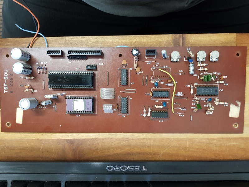
There was no sound. I started probing around the 8035 and found it was giving out garbage. I pulled the 2708 ROM and found that also full of garbage. I did try erasing it and reprogramming but it wouldn’t program at all. I replaced this with a slightly modified 2732 EPROM.
I ordered a new 8035 and while waiting I decided the best course of action would be to refurb this whole PCB as much as I could. All capacitors were replaced and replaced some of the logic IC’s too just for good measure.
Found a few dodgy looking solder joints like this one along the way

The replacement 8035 came from eBay but it was DOA. The seller send me another no questions asked and this one worked fine.
That’s about it for this one.

Worth noting with this conversion that it was been wired to use the player 2 joystick as the aiming function for player 1.

 Posted by at 7:45 pm

Site Donations

 General  Comments Off on Site Donations
May 312019
 

Well,
Just a few hours after getting the site back up and making a post on here and twitter about the possibility of donations I can safely say that all costs have been met for the full year.

I am stunned at the level of support received on this.
Asking for donations is something I never wanted to publicly ask for but its gone so much better than I expected.

Once again massive thanks to:
Banjo Guy Ollie
Caius
IronGiant/VectorGlow
Derick2k

 Posted by at 7:27 pm