Scramble (bootleg) repair log

 PCB Repair Logs  Comments Off on Scramble (bootleg) repair log
Apr 092019
 

Hammy sent me a couple of boxes of PCB’s recently. Among them was this Scramble bootleg PCB.

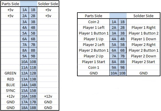
I’m still not sure if this pinout is unique but I had to figure this one out for myself.
Finding the VCC and GND pins is easy enough and just a matter of checking continuity from a know IC.
Once I had the power pins hooked up I fired it up and used the scope to probe for video signals. As long as the board boots the RGB should be easy to identify and as long as sync is being generated we should be able to find a 15khz signal somewhere.
Fortunately for me that is exactly what I found so I hooked them up and got this

I already knew this game didn’t match anything in MAME but I pulled all the ROM’s anyway and dumped them.
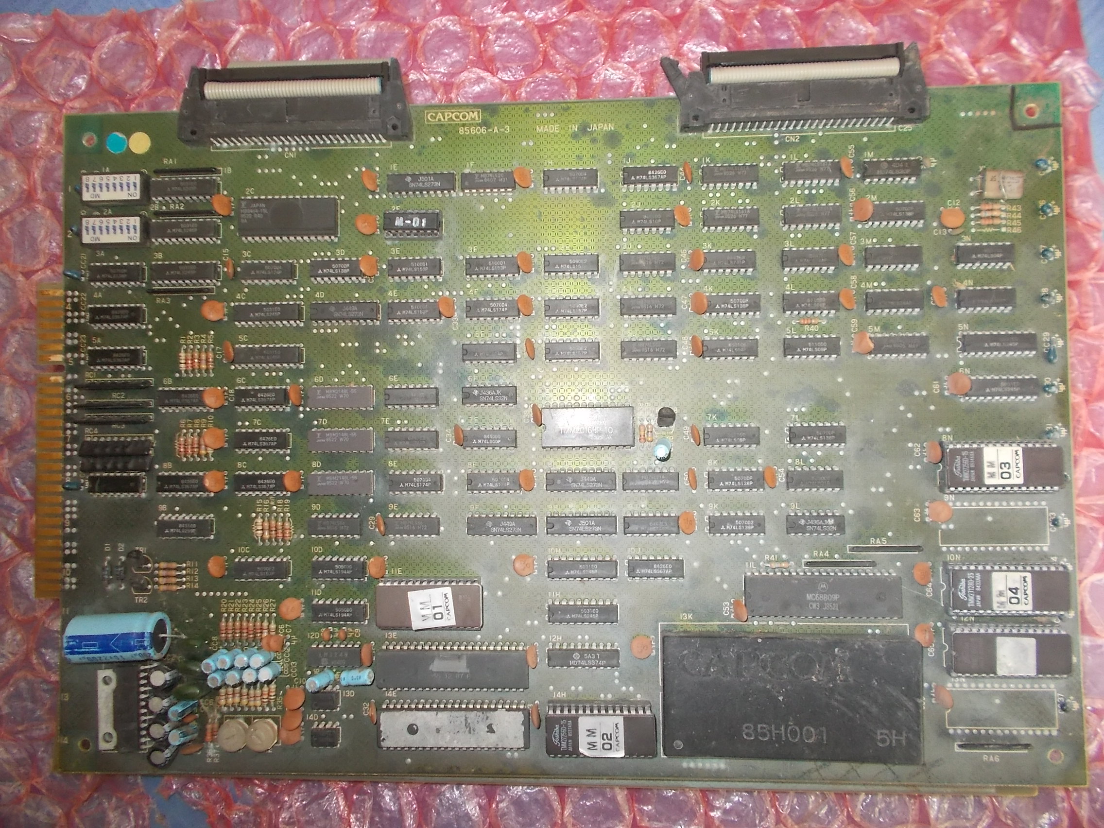
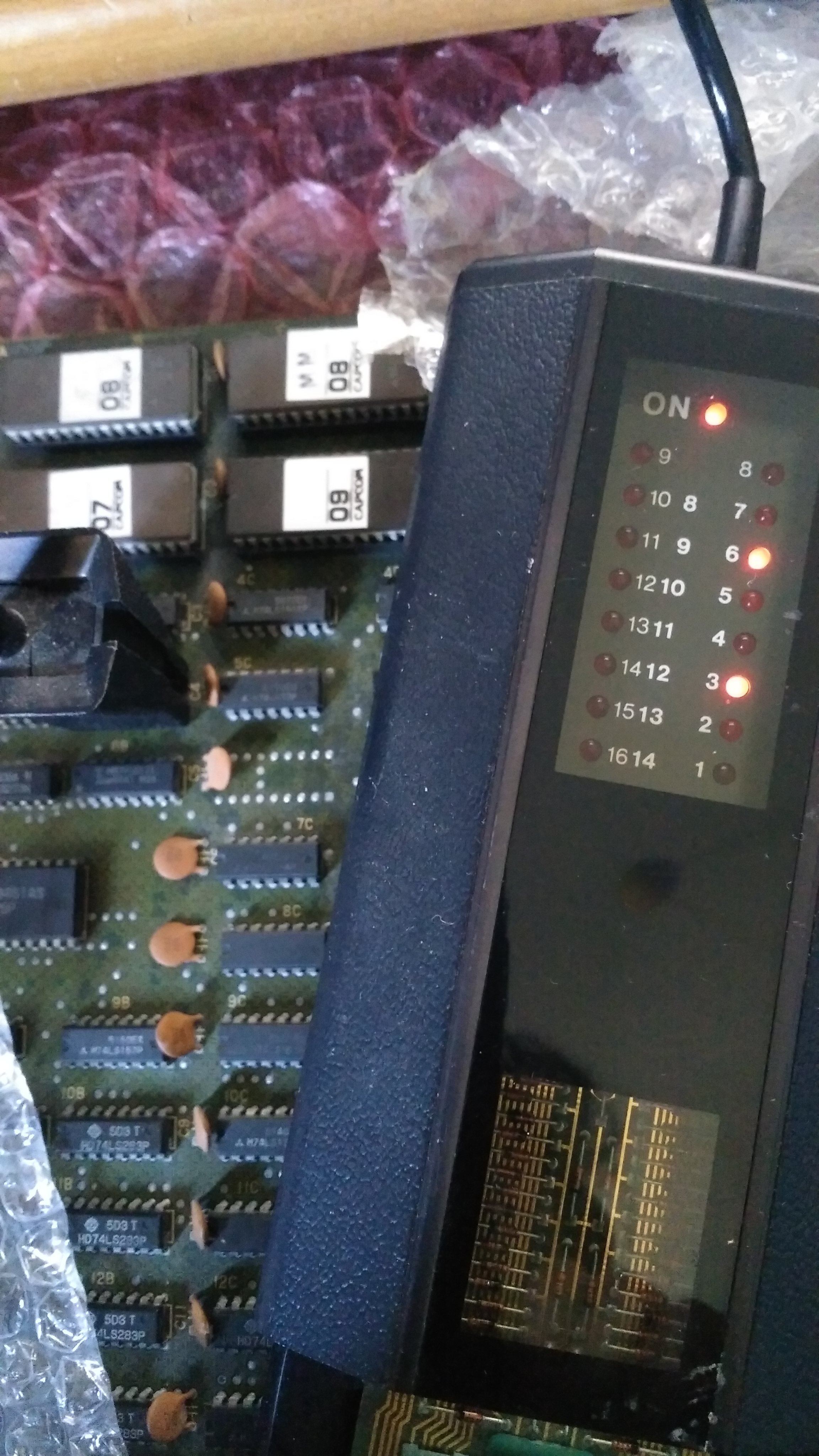
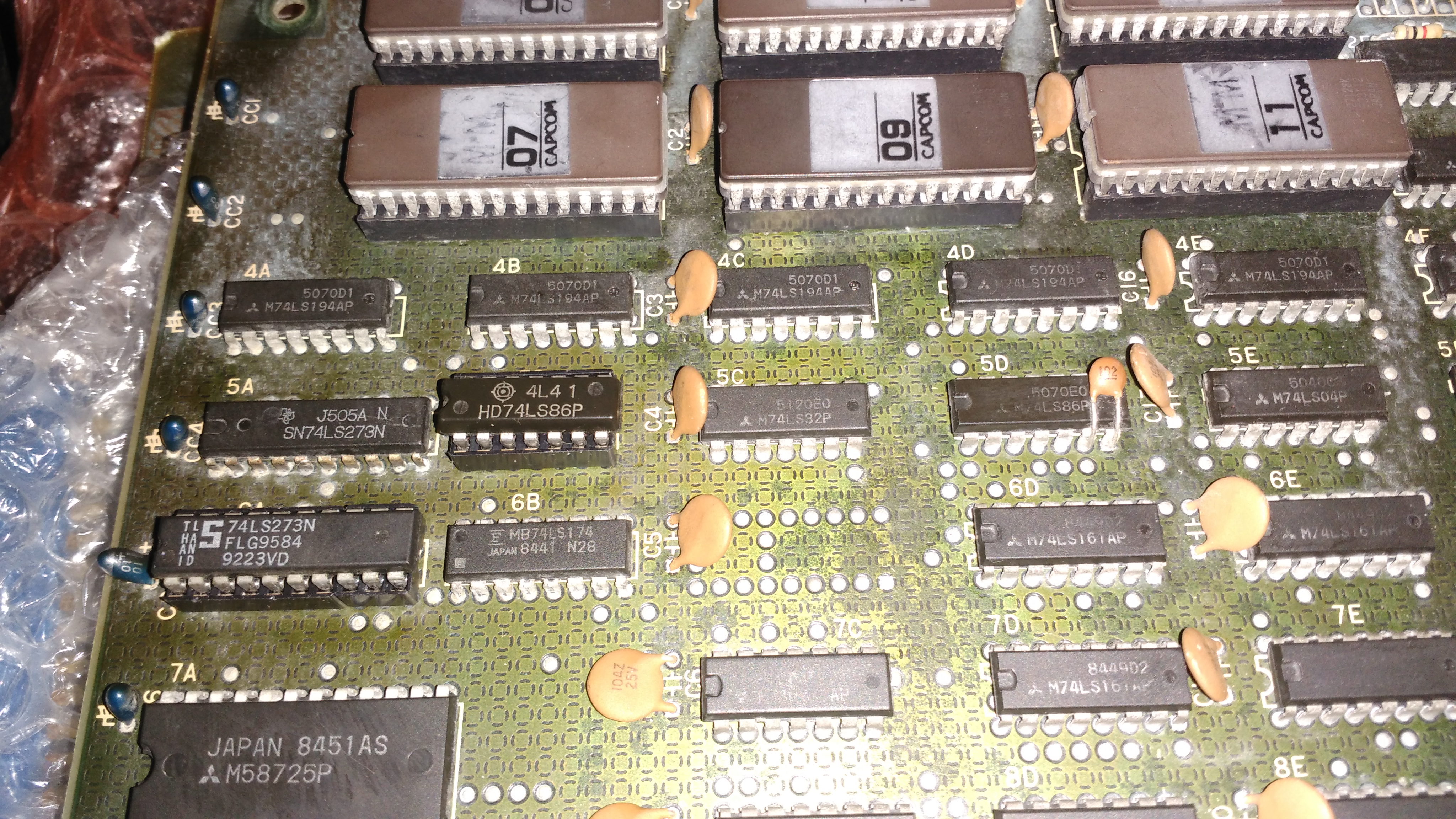
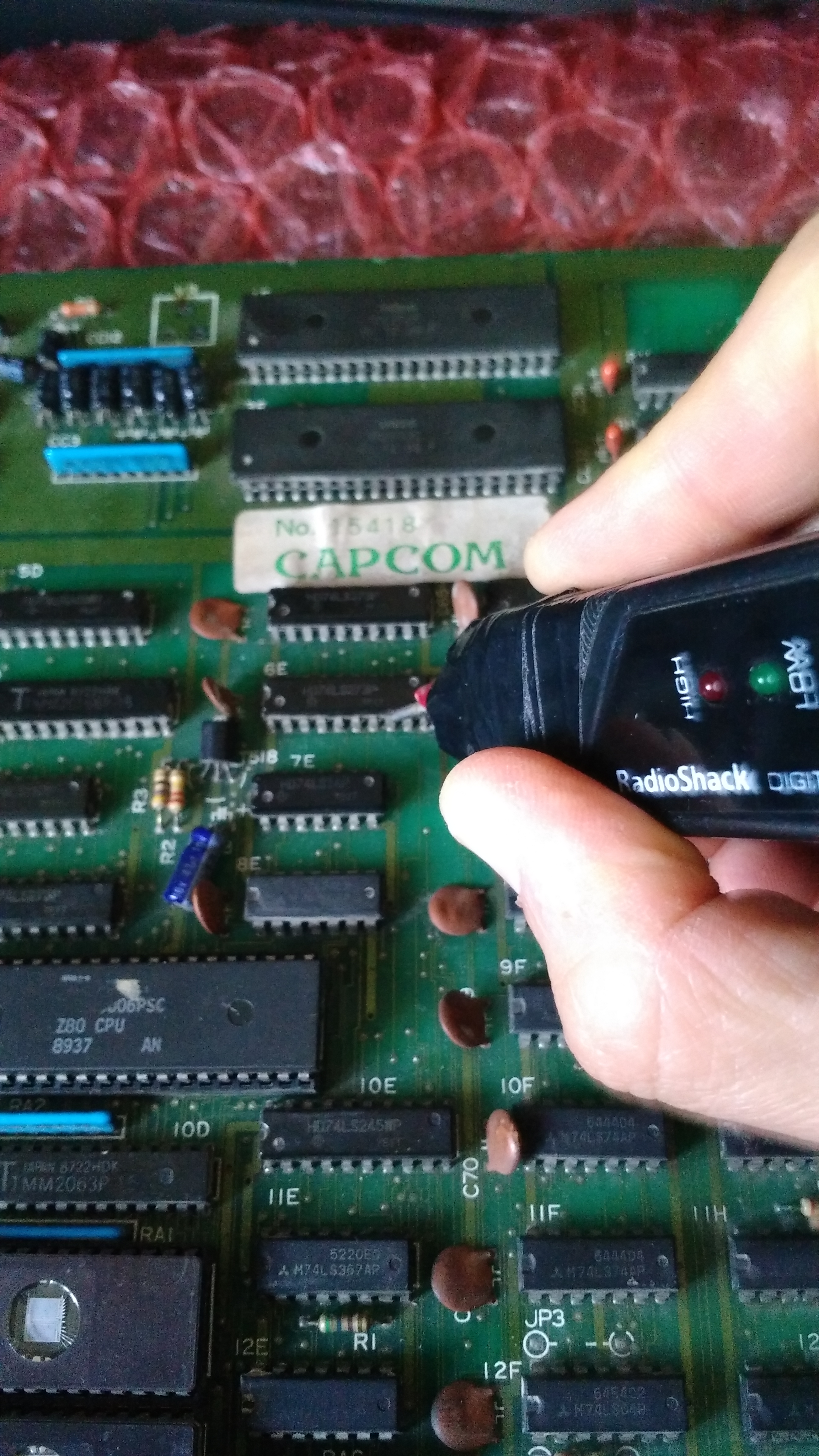
The Z80 is socketed on this PCB so I plugged the Fluke 9010 in and carried out the ROM tests. All the ROM’s could be read without a problem.
Next on to the RAM.

I originally looked at the wrong MAME source for this board. I looked at galaxian.cpp but I should have been referring to galaxold.cpp. Because of this error I ended up wasting a bit of time looking for a fault that didnt exist.
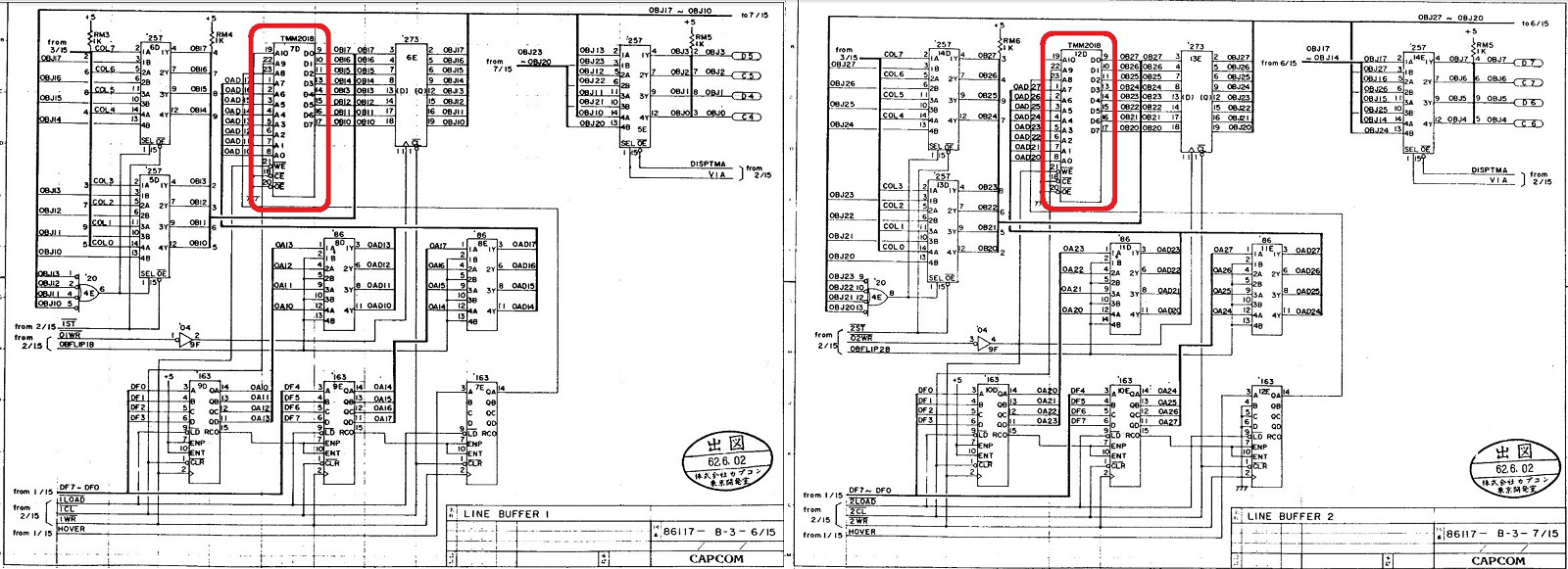
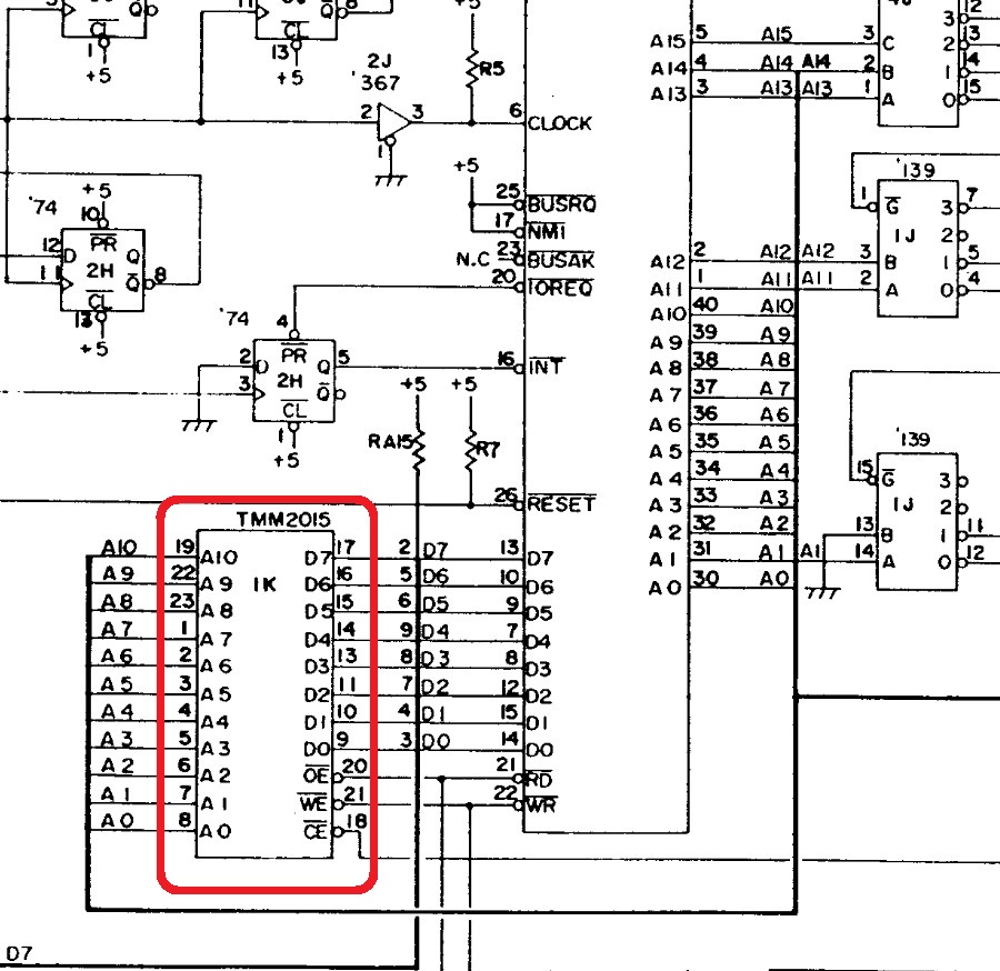
One this PCB the work RAM is between addresses $4000 – $47ff.
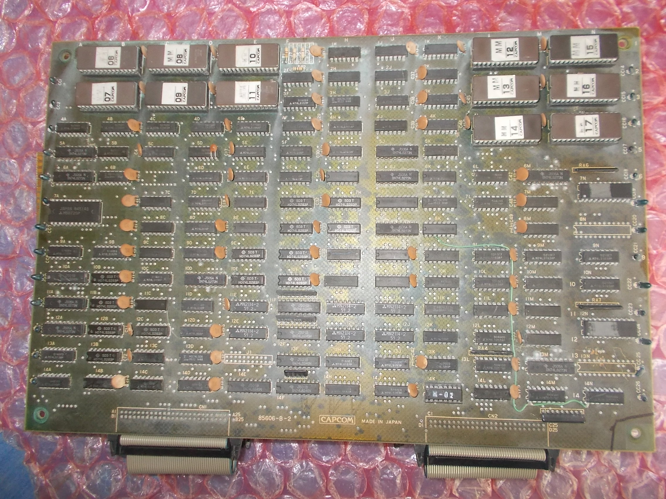
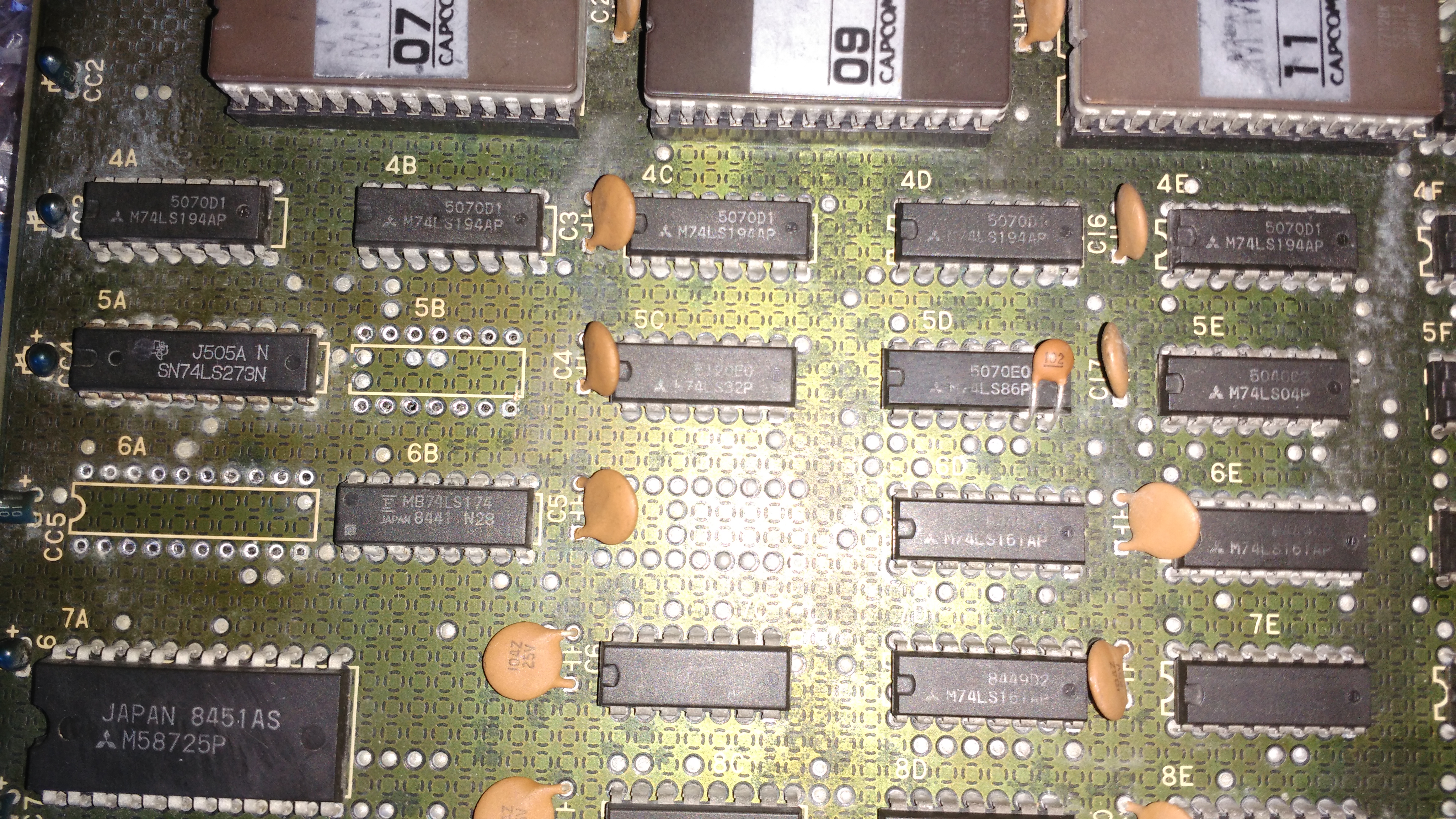
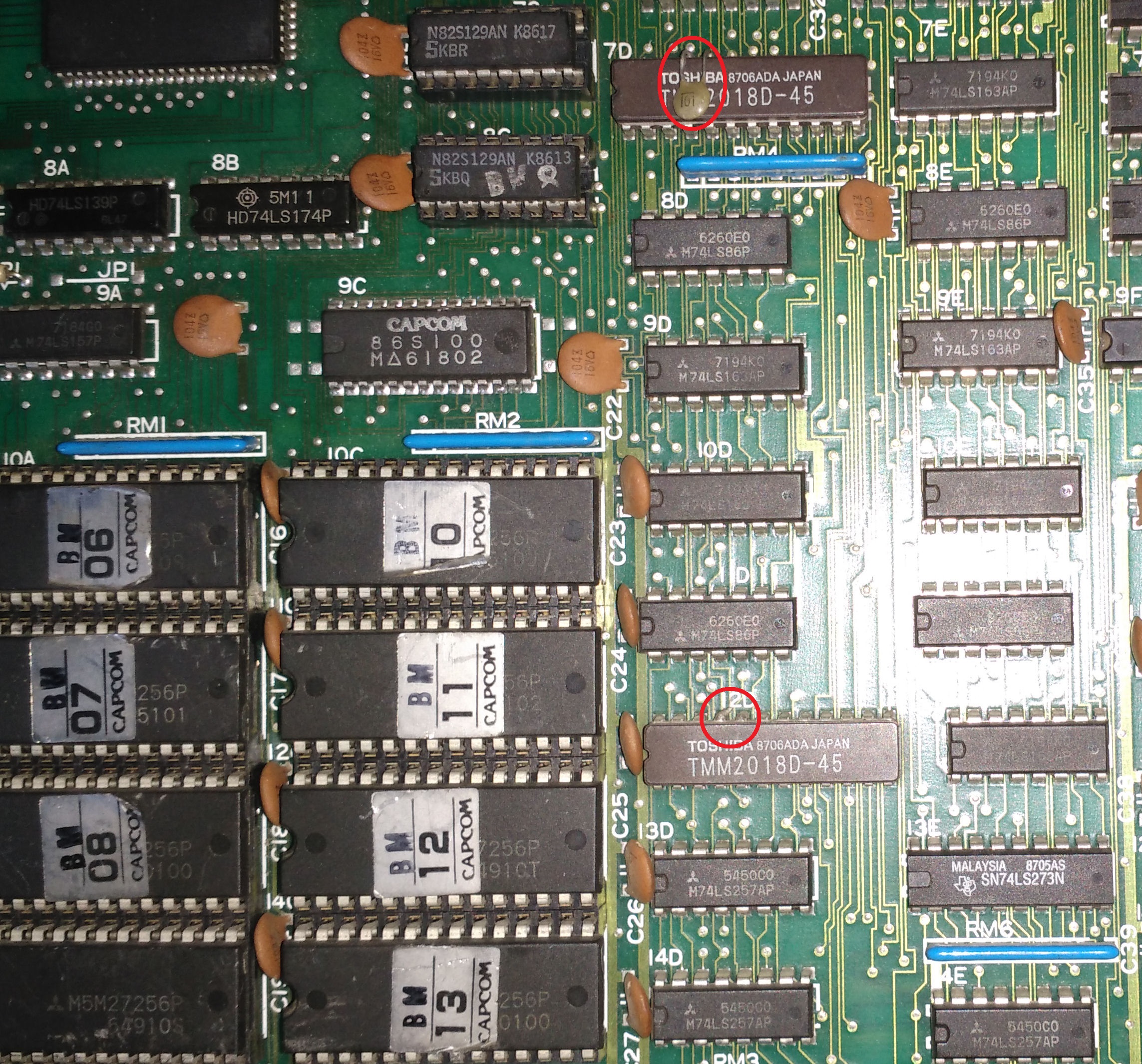
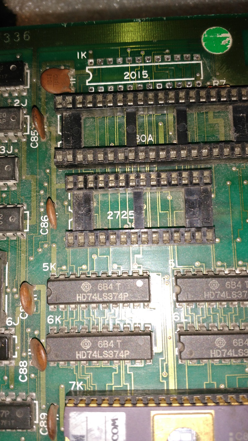
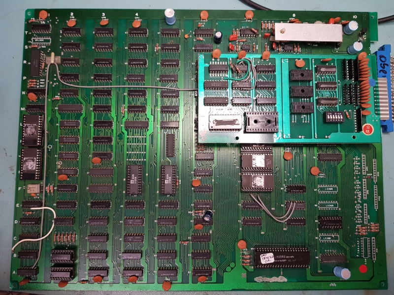
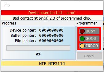
On the riser PCB I could see 2 x 2114 RAM’s which are a 4 bit memory but this would only give me 1024 (0x3ff)bytes on RAM and I was expecting double that. Removing the riser board revealed the second set of 2114 chips.
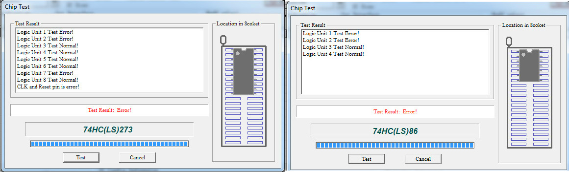
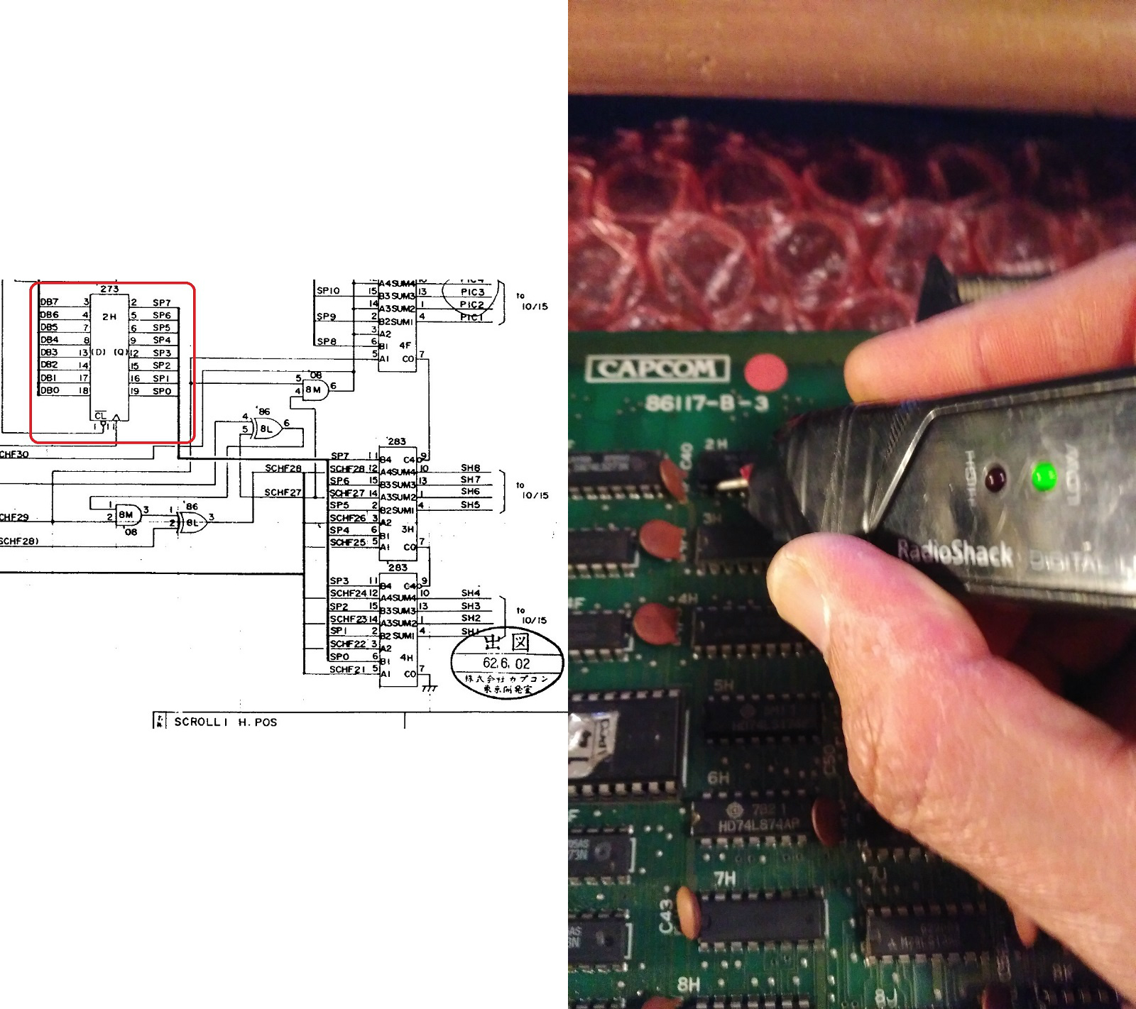
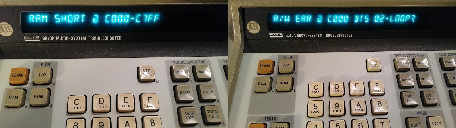
Running the RAM check on the Fluke gave me RAM errors in the upper half of the range which I determined was on the riser PCB. I removed both of them to be sure and found one was giving errors on 2 address pins

Replacing this gave me this

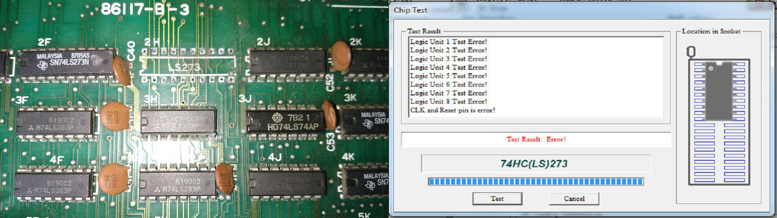
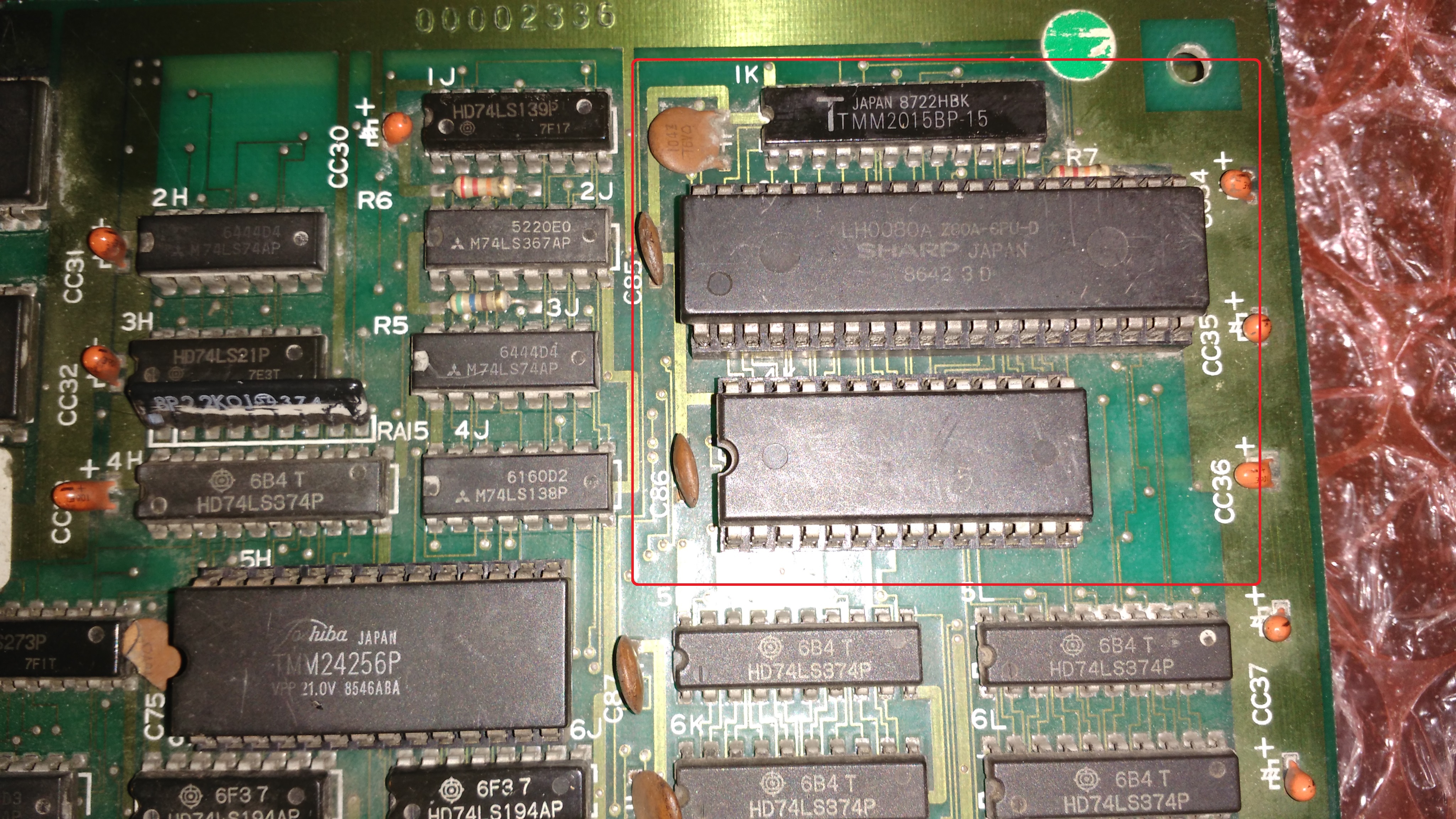
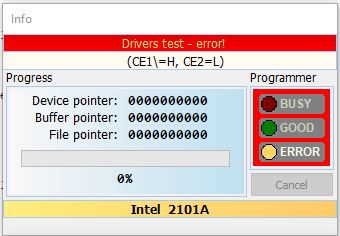
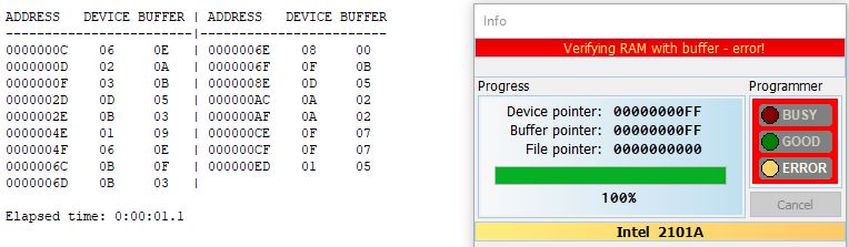
Error 3 doesn’t exactly give me much to work with so I just went round the other RAM ranges. There is some screen RAM at address range $5000 – $50ff. This failed.
This RAM in 2 x 2101 and as luck would have it it is already socketed.
I removed both and tested them and both failed

I have plenty of these spare due to my dealings with early Nintendo boards so swapped them right out.
We have success and with the audio hooked up we get this.

The riser board on this thing seems to be for the control inputs
Here is the pinouts I got for the PCB. There is likely a few things missing like coin counter but I’m not bothered about that.

 Posted by at 1:46 pm

Ghosts’n Goblins repair log #2

 PCB Repair Logs  Comments Off on Ghosts’n Goblins repair log #2
Apr 062019
 

Got for repair from USA this faulty original Ghosts’n Goblins PCB, a two stack made of a CPU board :

And a VIDEO board:

Both boards were very dirty especially on solder side:

Some areas were corroded too:

Before applying power I washed both boards and neutralized the corrosion with some vinegar.On smoke test the game booted up, it was playable with sound too but with noticeable graphical issues :

I polished the contacts inside the connectors of the ribbon cables and the big vertical bars disappeared but backgrounds were kinda pixelated :

The circuit which generates the tiles lies on VIDEO board and it’s labeled as “SCROLL” in schematics (last three pages of PDF).Checking it with a logic probe I quickly found a 74LS273 @6A with a dead output:

The scope confirmed the output (pin 15) was floating while input (pin 14) was toggling:

The signal from this dead output is called ‘SVFLIP’ in snippets of above schematics and it’s routed to the inputs of a 74LS86 @5B which outputs some address lines for the backgounds ROMs:

Probing the 74LS86 @5B with my HP10529A logic comparator revealed troubles on output pin 3 and 6:

I removed it along with the 74LS273 @6A :

Both chips failed the out-of-circuit testing :

I installed sockets with good chips :

Backgounds were so restored and board 100% fixed.End of job.


 Posted by at 10:36 pm

1943 : Midway Kaisen repair log

 PCB Repair Logs  Comments Off on 1943 : Midway Kaisen repair log
Apr 042019
 

Received for repair from Germany a ‘1943 : Midway Kaisen’ PCB (same hardware of export version ‘1943 : The Battle of Midway’ but with japanese ROM set).

Set is made of a CPU board :

And a VIDEO board:

The board was faulty, it showed graphic errors and had no sound :

Specifically the graphic faults concerned the text (also called “characters”), the scrolling and the sprites.Let’s go in order.


  • The text/characters issue.

The text had wrong colors, here is how it looked like:


Whereas it should have been (snapshot from MAME)

Schematics in hand I started to check the revelant circuit with my logic probe and found a stuck signal on an address line of the BPROM @7F on CPU board:

This signal is labeled ‘CC3’ on schematics :

I traced it back to the input (pin 8) of two 74LS273 :


Signal was toggling on the one @5E but absent on 6E:

There was clearly a broken trace somewhere between pin 8 of the two 74LS273 so I ran a jumper wire on solder side, this restored the correct text :


  • The scrolling issue.

The problem showed itself like some of the backgrounds (like clouds) were fixed  :

Looking at schematics there are on VIDEO board two separate circuits for horizontal and vertical scrolling.Checking them I found a 74LS273 @2H with stuck ouptuts :

I removed the chip and tested it out-of-circuit, it failed as expected:

I installed a good IC and scrolling came back to normal.


  • The sprite issue.

Most of objects were fine but some of them (like bullets) sometimes turned into squared blocks:

Sprites data are stored in eight 27256 OTP ROMs:

I read them and dumps turned out to be good but as further proof I swapped the devices one by one with a good set from another same board.When I swapped the one @10A labeled ‘BM06’ the issue disappeared so I programmed a blank 27256 EPROM.Sprites were fine now but there were still some little glitches affecting them :

The sprites line buffer is made of two identical circuits called “LINE BUFFER 1” and “LINE BUFFER 2” in the schematics.Two 2K  x8-bit static RAMs (TMM2018) are the main part of this circuit :

Probing around I found nothing of abnormal but I noticed that a 100pF ceramic capacitor was installed between pin 20 (/OE tied to GROUND) and pin 21 (/WE)  of one RAM whereas the other chip lacked of it (but I could see some solder residuals so perhaps the capacitor was present but then came off)

I installed the missing capacitor and this cleared the glitches,  sprites were perfectly displayed now.

Last issue to troubleshoot was the lack of audio.The 1K potentiometer was missing :

Fitting it did not restore the sound, the fault was in the digital part of the circuit made of a Z80 CPU, a 27256 ROM and a 2k x 8-bit SRAM (Toshiba TMM2015)

The ROM was dumped as good so I fired up my Fluke 9010A troubleshooter and launched a RAM test which reported an ‘R/W ERR @ C000 BTS 02’ of the TMM2015 @1K  :

This means the Fluke encountered an error at address 0xC000 (the start of the Z80 address space where the RAM lies) where it was unable to read/write ‘bit 02’ which turned from hex number to binary is ‘00000010’.Translated into hardware this means that data line ‘D1’ of the TMM2015 SRAM was not working hence chip was likely faulty:

I pulled the RAM:

Chip failed the out-of-circuit test :

Fitting a good RAM chip restored the sound and fixed the board completely.Job done.


 Posted by at 12:10 pm