Been doing a few bits with muddymusic’s Jumping PCB.
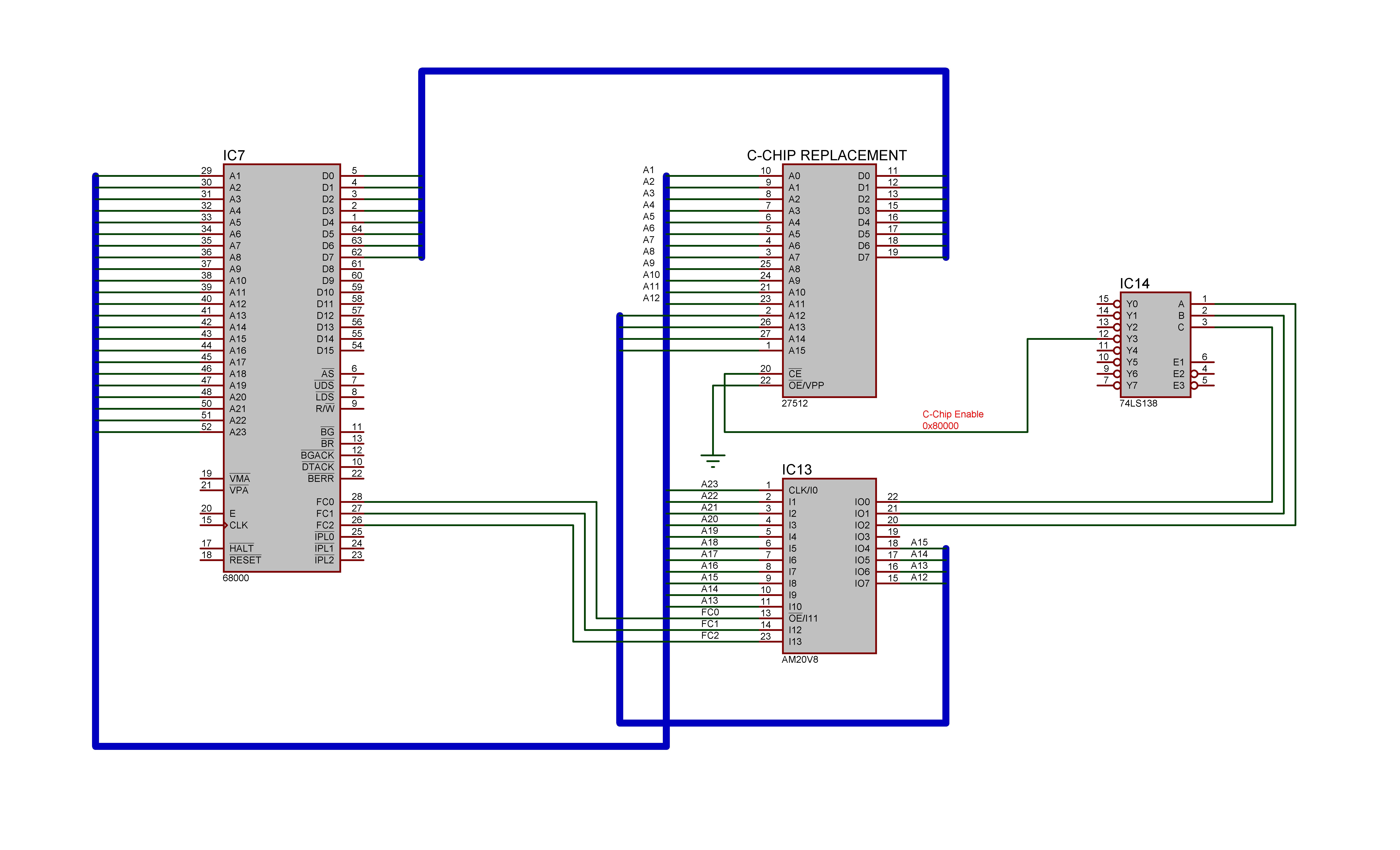
I wanted to see how the C-Chip substitute ROM was wired into the circuit so ive made a small schematic and reversed the address decoder PAL.
Here are the equations for the address decoder too. Ive renamed to the pins to something more suitable for human consumption.
/* Inputs */
Pin 1 = A23;
Pin 2 = A22;
Pin 3 = A21;
Pin 4 = A20;
Pin 5 = A19;
Pin 6 = A18;
Pin 7 = A17;
Pin 8 = A16;
Pin 9 = A15;
Pin 10 = A14;
Pin 11 = A13;
Pin 13 = FC0;
Pin 14 = FC1;
Pin 23 = FC2;
/* Outputs */
Pin 15 = CA12; /* A12 of C-Chip replacement ROM */
Pin 16 = CA13; /* A13 of C-Chip replacement ROM */
Pin 17 = CA14; /* A14 of C-Chip replacement ROM */
Pin 18 = CA15; /* A15 of C-Chip replacement ROM */
Pin 19 = LROM; /* Chip enable for other ROM’s */
Pin 20 = A; /* Pin 1 of 74LS138. Input A */
Pin 21 = B; /* Pin 2 of 74LS138. Input B */
Pin 22 = C; /* Pin 3 of 74LS138. Input C */
/* Equations */
!CA12 = !A23 & !A22 & !A21 & !A20 & !A19 & !A13 #
!A23 & !A22 & !A21 & A20 & !A19 & !A18 & !A17 & !A16 & A15 & A14 & !A13 #
!A23 & A22 & !A21 & !A20 & !A19 & !A18 & !A17 #
!A23 & A22 & !A21 & !A20 & !A19 & !A18 & A17 & A16 #
A23 & A22 & !A21 & !A20 & !A19 & !A18 & !A17 & !A16 & !A13 #
!A23 & !A22 & !A21 & !A20 & A19 & !A18 & !A17 & !A13 #
A23 & A22 & !A21 & A20 & !A19 & !A18 & !A17 & !A16 & !A15 & !A14 & !A13;
!CA13 = !A23 & !A22 & !A21 & !A20 & !A19 & !A14 #
!A23 & A22 & !A21 & !A20 & !A19 & !A18 & A17 #
A23 & A22 & !A21 & !A20 & !A19 & !A18 & !A17 & !A16 & !A14 #
!A23 & !A22 & !A21 & !A20 & A19 & !A18 & !A17 & !A14;
!CA14 = !A23 & !A22 & !A21 & !A20 & !A19 & !A15 #
A23 & A22 & !A21 & !A20 & !A19 & !A18 & !A17 & !A16 & !A15 #
!A23 & !A22 & !A21 & !A20 & A19 & !A18 & !A17 & !A15;
!CA15 = !A23 & !A22 & !A21 & !A20 & !A16;
!LROM = !A23 & !A22 & !A21 & !A20 & !A17;
!A = !A23 & !A22 & !A21 & !A20 & !A19 & !A18 #
!A23 & !A22 & !A21 & A20 & !A19 & !A18 & !A17 & !A16 & A15 & A14 #
!A23 & !A22 & A21 & !A20 & !A19 & !A18 & !A17 & !A16 & !A15 & !A14 & !A13 #
A23 & A22 & !A21 & !A20 & !A19 & !A18 & !A17 & !A16 #
A23 & A22 & !A21 & A20 & !A19 & !A18 & !A17 & !A16 & !A15 & !A14 & !A13;
!B = !A23 & !A22 & !A21 & !A20 & !A19 #
A23 & A22 & !A21 & !A20 & !A19 & !A18 & !A17 & !A16 #
!A23 & A22 & !A21 & !A20 & !A19 & A18 & !A17 & !A16 #
A23 & A22 & !A21 & A20 & !A19 & !A18 & !A17 & !A16 & !A15 & !A14 & !A13;
!C = !A23 & !A22 & !A21 & !A20 & !A19 #
!A23 & !A22 & !A21 & A20 & !A19 & !A18 & !A17 & !A16 & A15 & A14 #
!A23 & !A22 & !A21 & !A20 & A19 & !A18 & !A17;
The A, B and C outputs from the PAL feed into a 74LS138. In order to select the C-Chip substitute A and B must be HIGH and C must be LOW. From the equations (or just looking at the MAME source code) we can work out that the C-Chip ROM lies at address 0x80000.
So, not a great deal of info but its pretty interesting all the same.

