PAL UpdatesComments Off on Kaneko Super Nova ROM board PAL dumps added
Oct232016
Found two ATF16V8 PLD’s in a Super Nova ROM cartridge. Both were unlocked but have not been verified as my PCB has a fault. The equations look good.
The ROM board is marked ROM-2.
PCB Repair LogsComments Off on Alpha Denshi Co. (Equites and Splendor Blast) double repair log
Oct182016
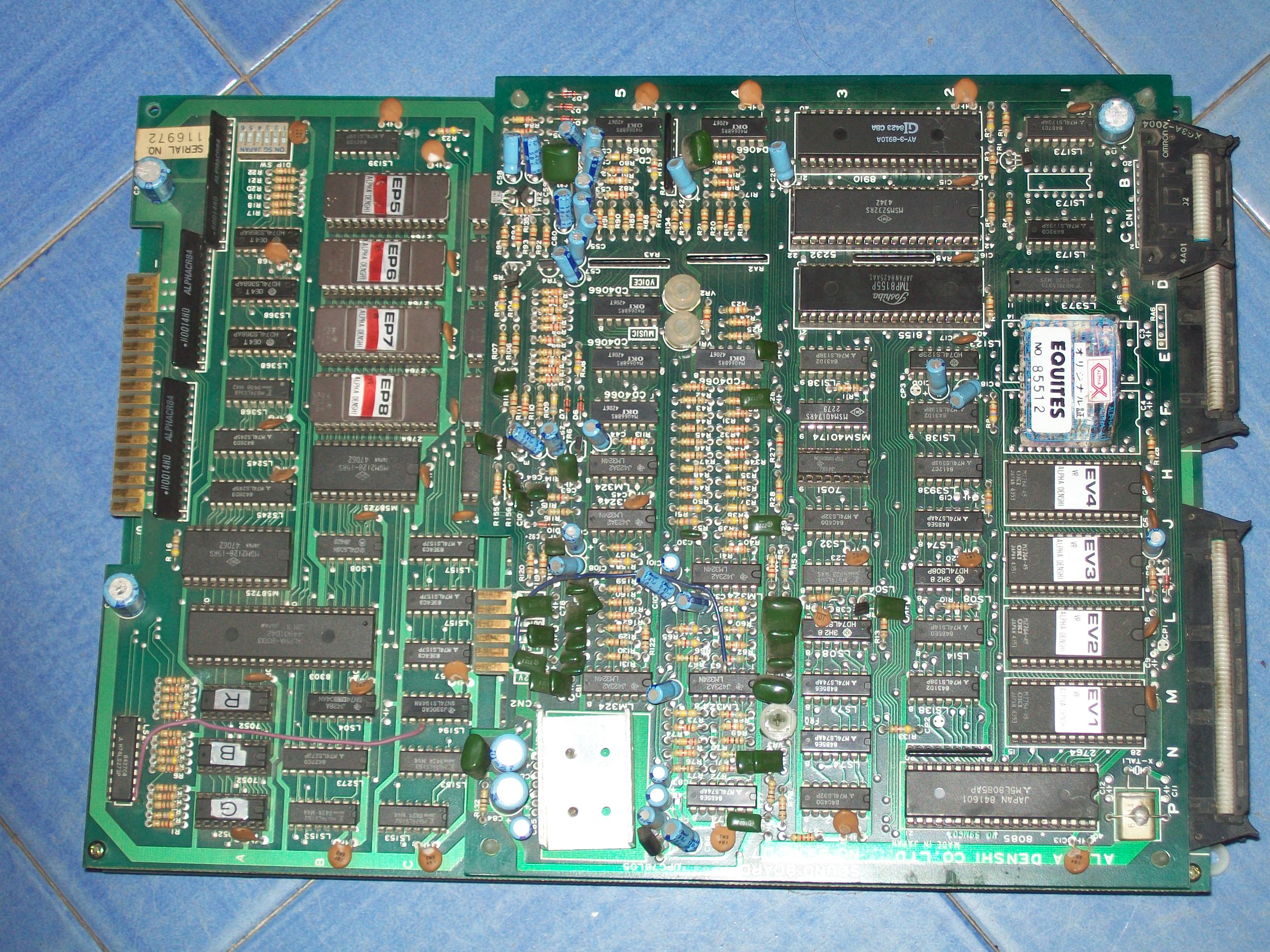
I got two rare boards manufactured by Alpha Denshi for repair : Equites and Splendor Blast
Here’s Equites :
Board played fine except for jailbars on some sprites (look at explosions and first enemies on the ground in the below video):
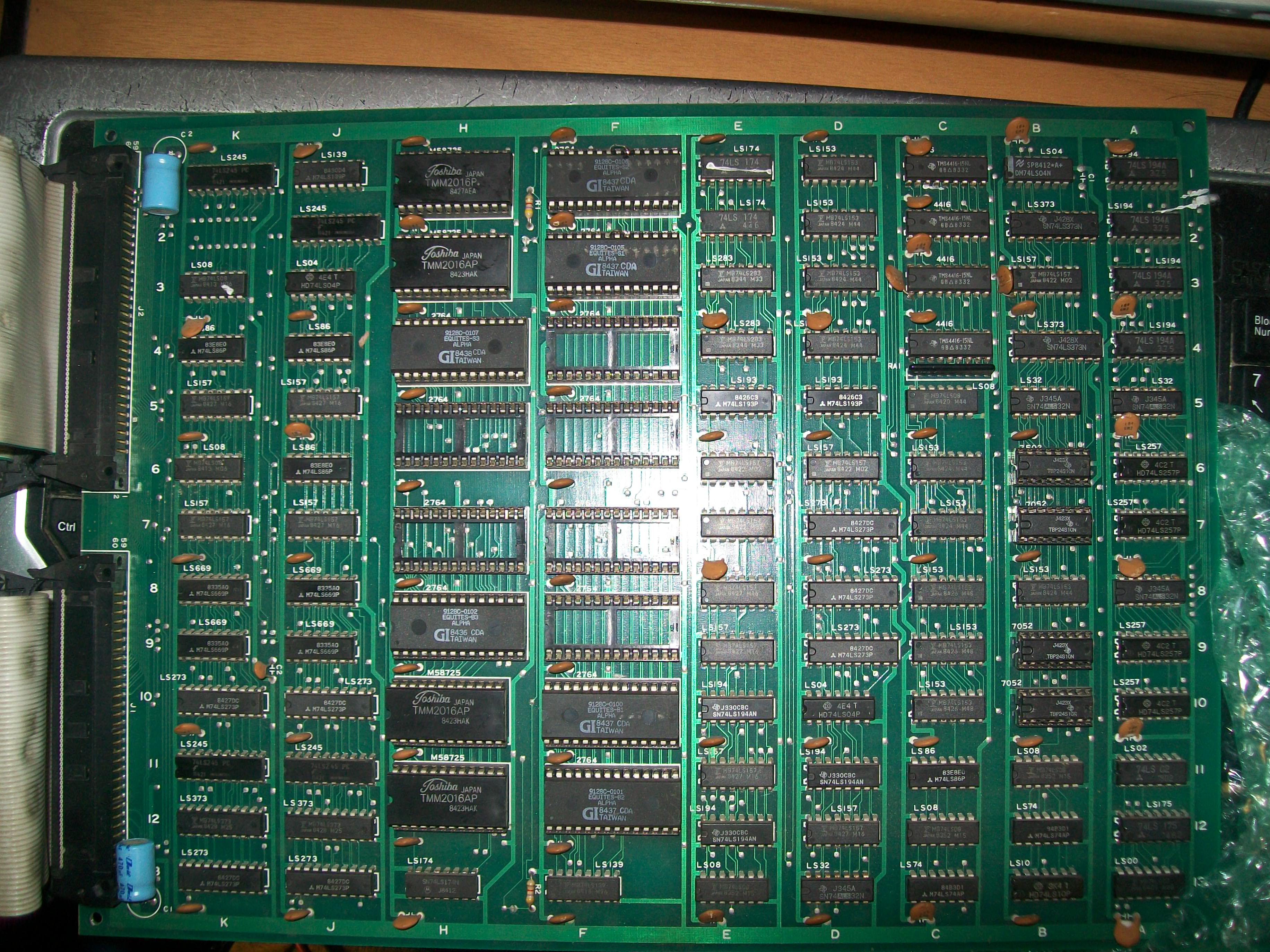
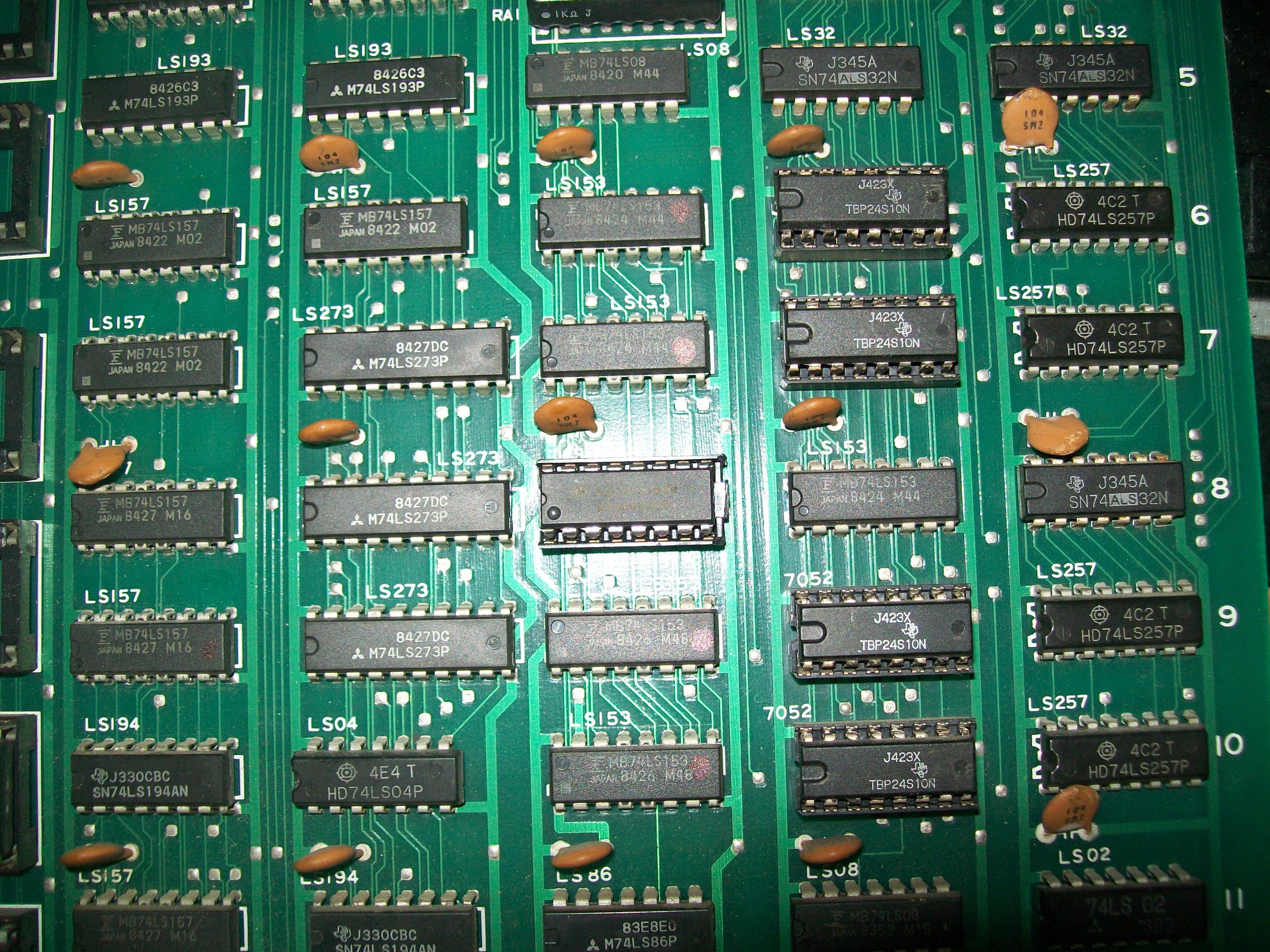
All the GFX generation circuitry lies on bottom board:
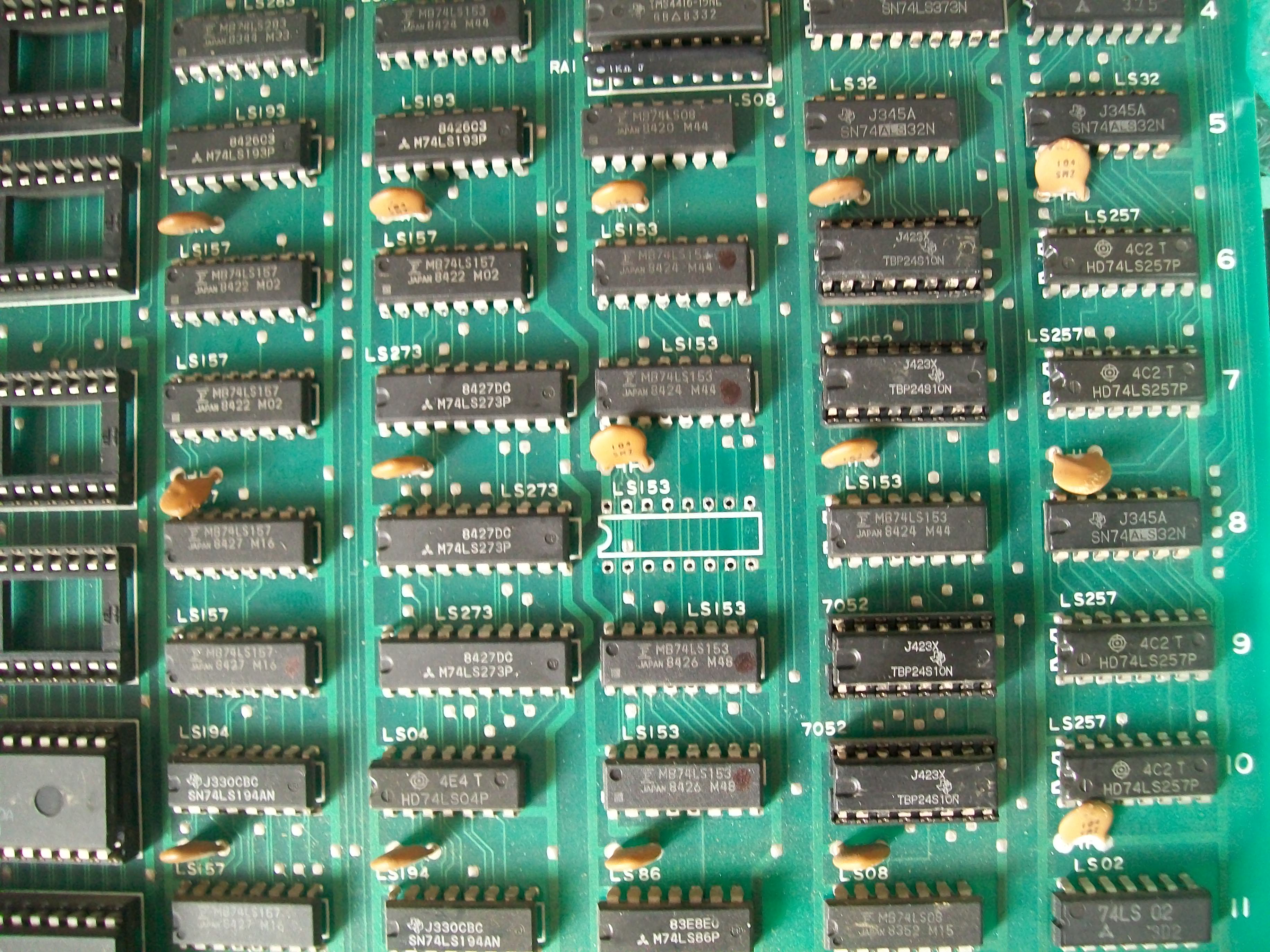
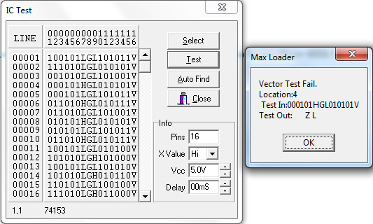
A lor of TTLs were from Fujitsu (especially multiplexers 74LS157 and 74LS153) so I went to check them with my logic comparator.All passed the test except for the 74LS153 @8C:
I desoldered it:
The chip failed when tested out-of-circuit:
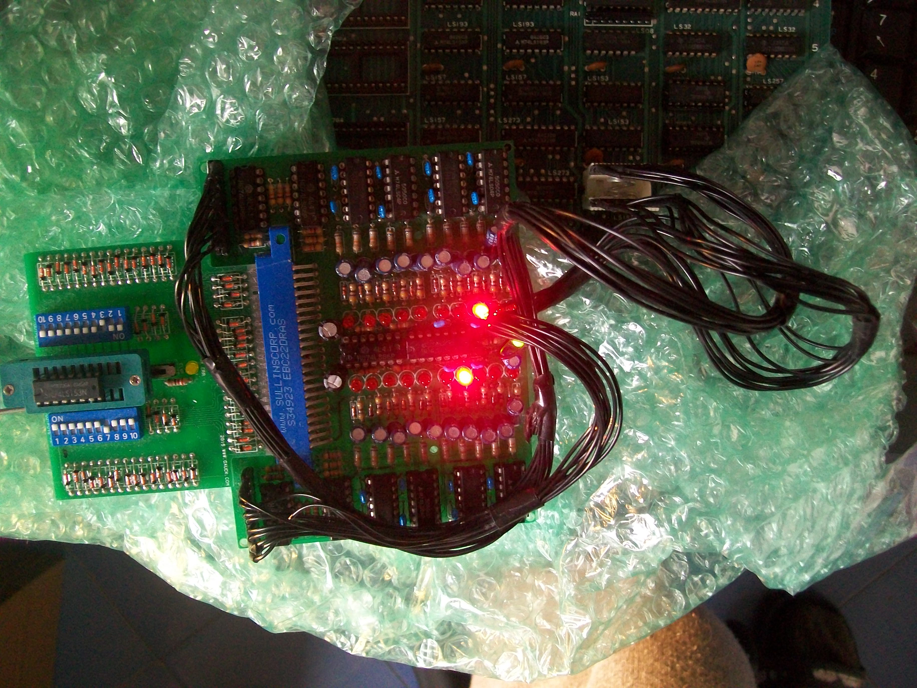
I added a socket and a good chip:
No more glitched sprites and board 100% fixed:
Here’s Splendor Blast:
This was a little tricky.When I first powered the board up, watchdog was active, the self-test was failing in all program ROMs and in the ‘ALPHA-8303’ MCU RAM:
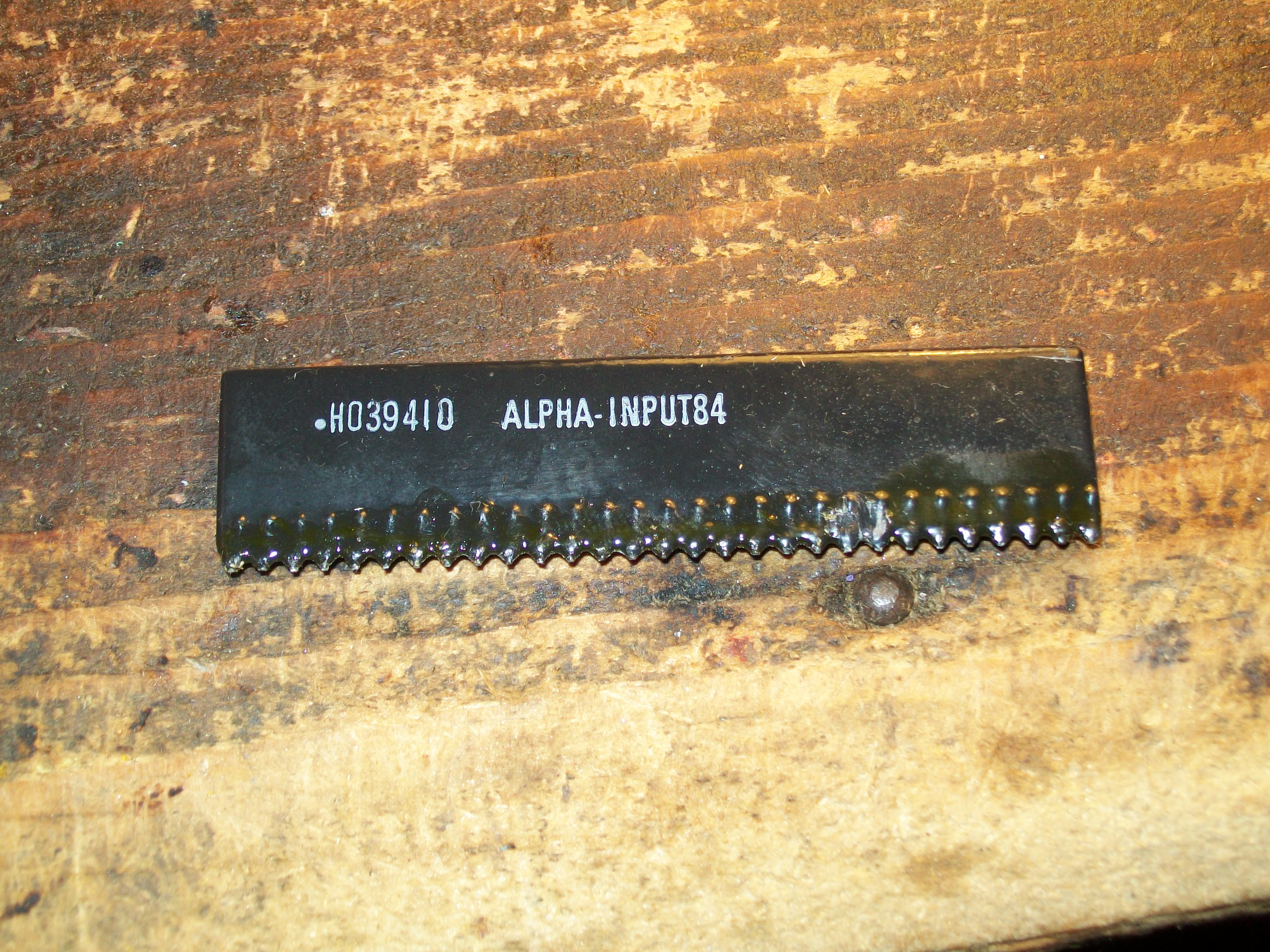
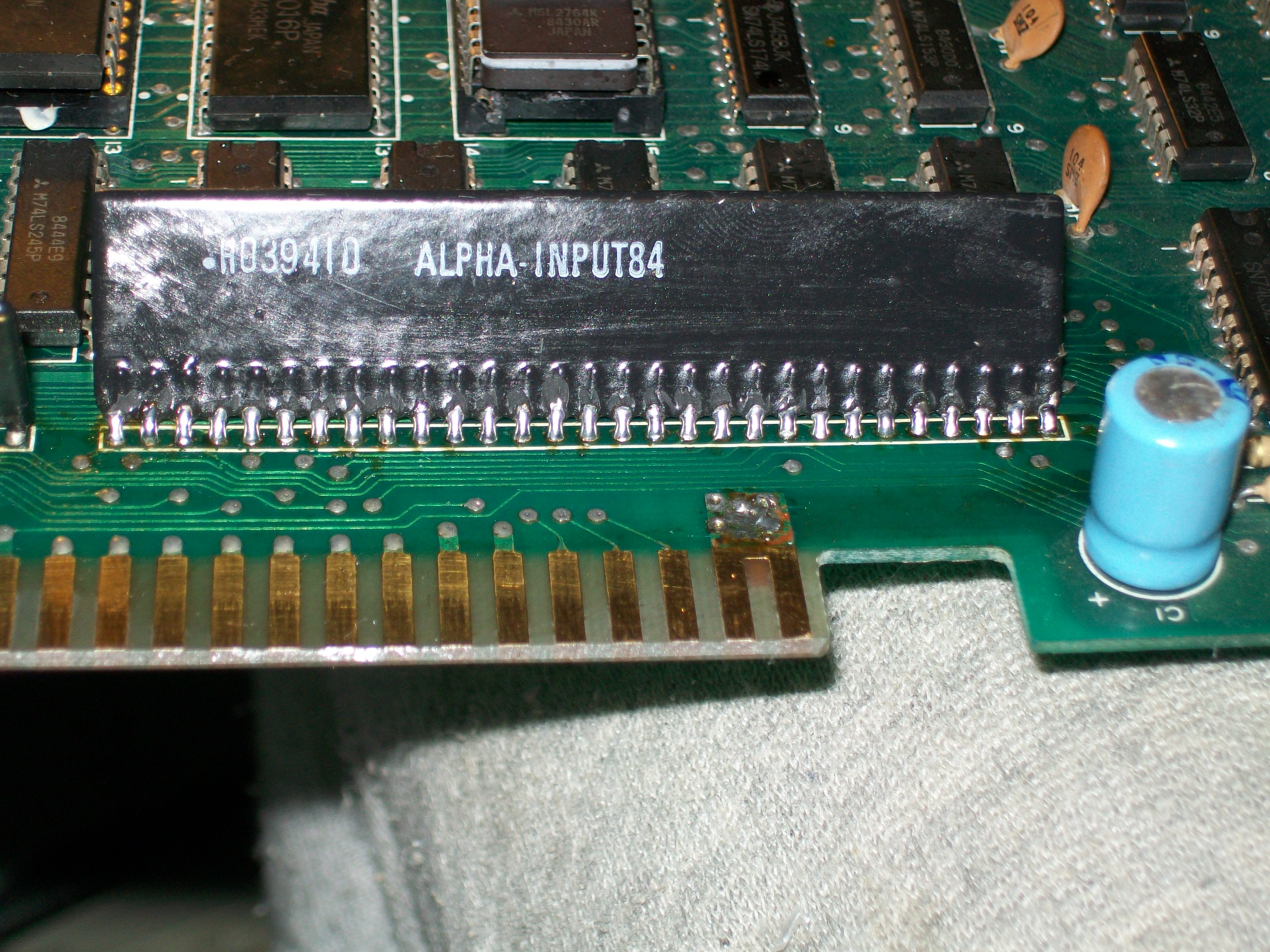
Doing a visual inspection of PCB I noticed that one of the two custom SIL marked ‘ALPHA-INPUT84’ was wonky :
It came off in my hands when I touched it:
I powered the board without this component and board successfully passed the self-test so I resoldered it (most likely it was corrupting the main 68000 CPU data bus since some lines are shared with it) :
As I said, the board entered in game but some sprites showed jailbars:
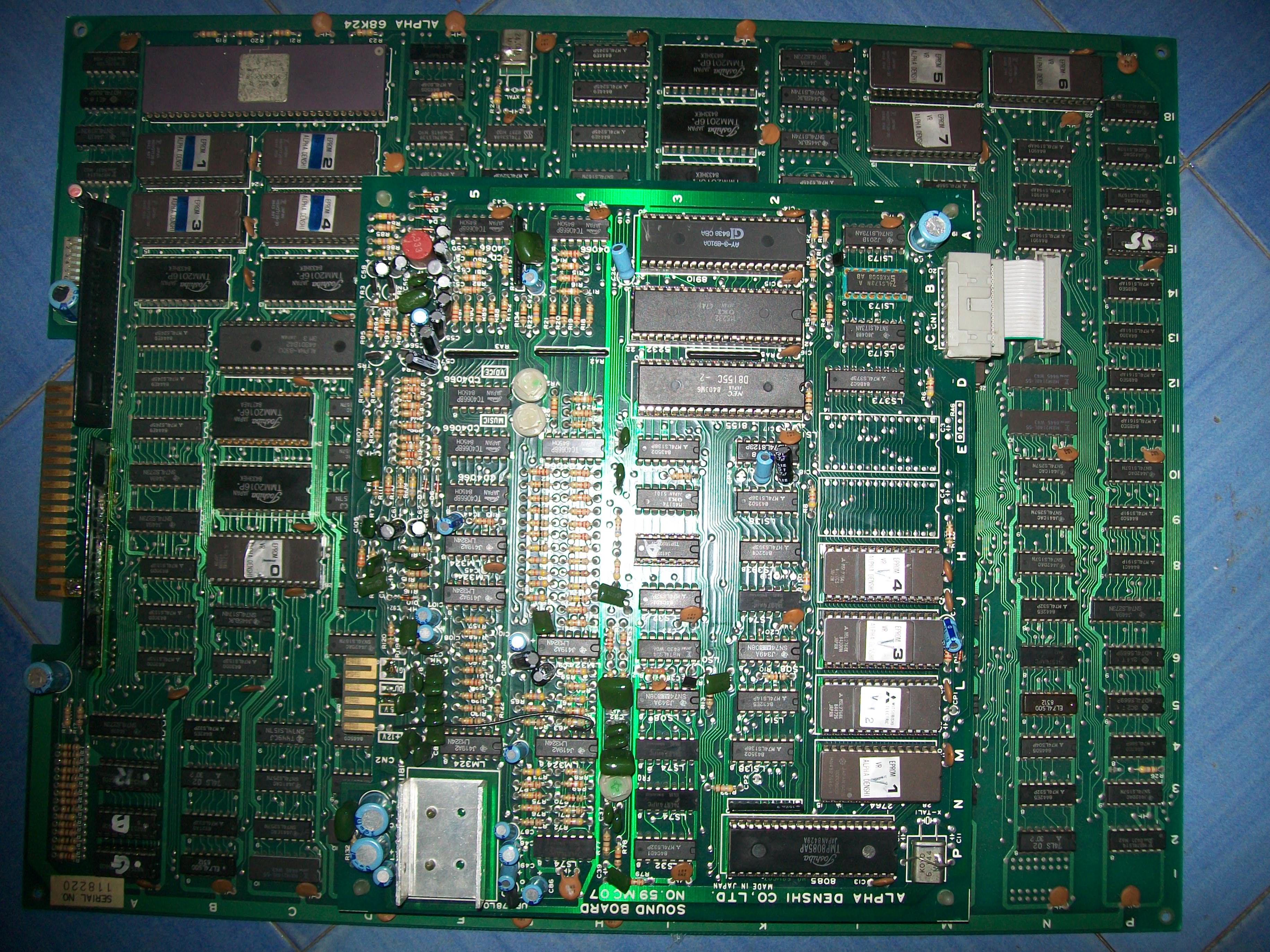
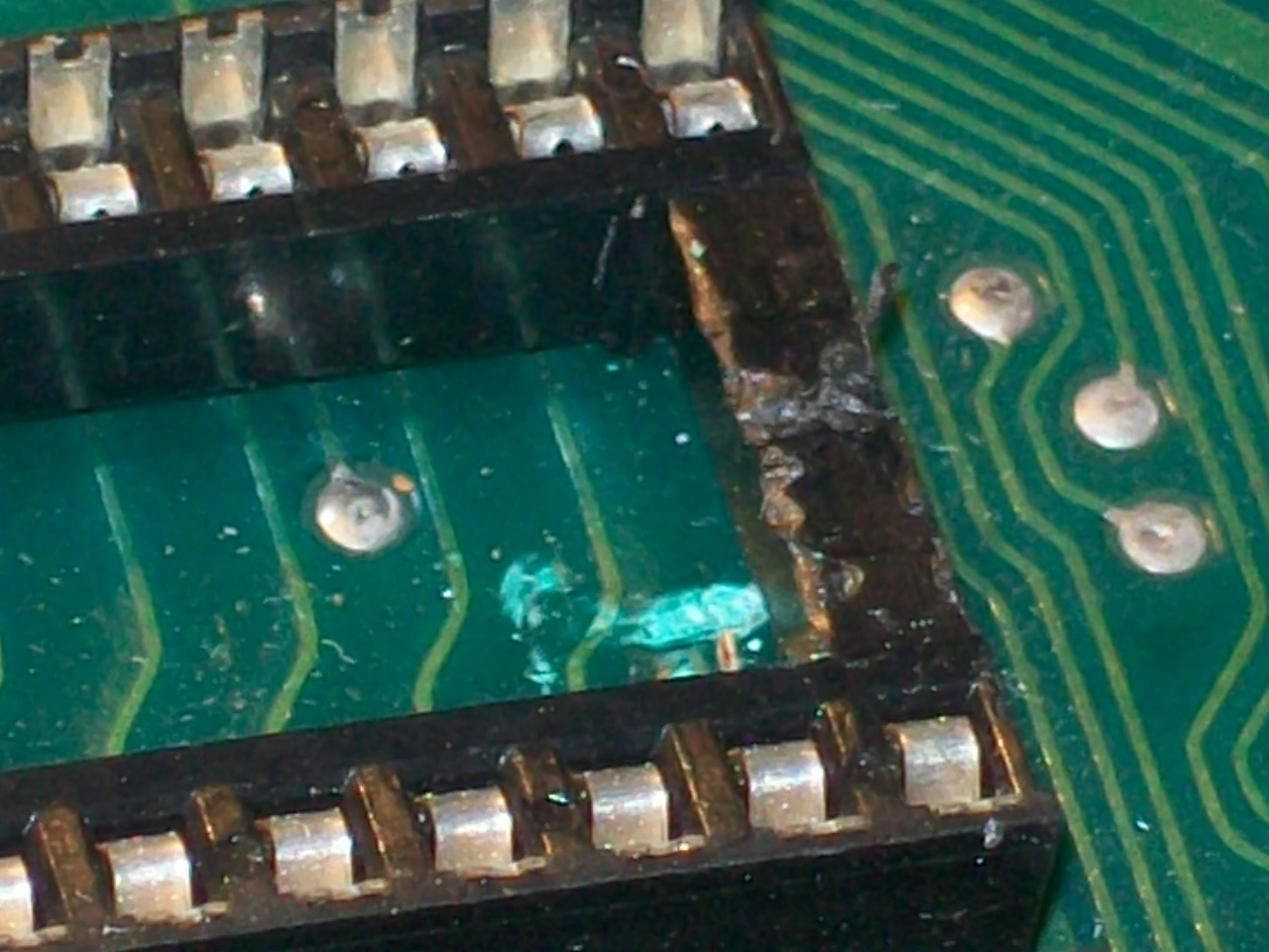
The three sprites ROMs are in bottom board:
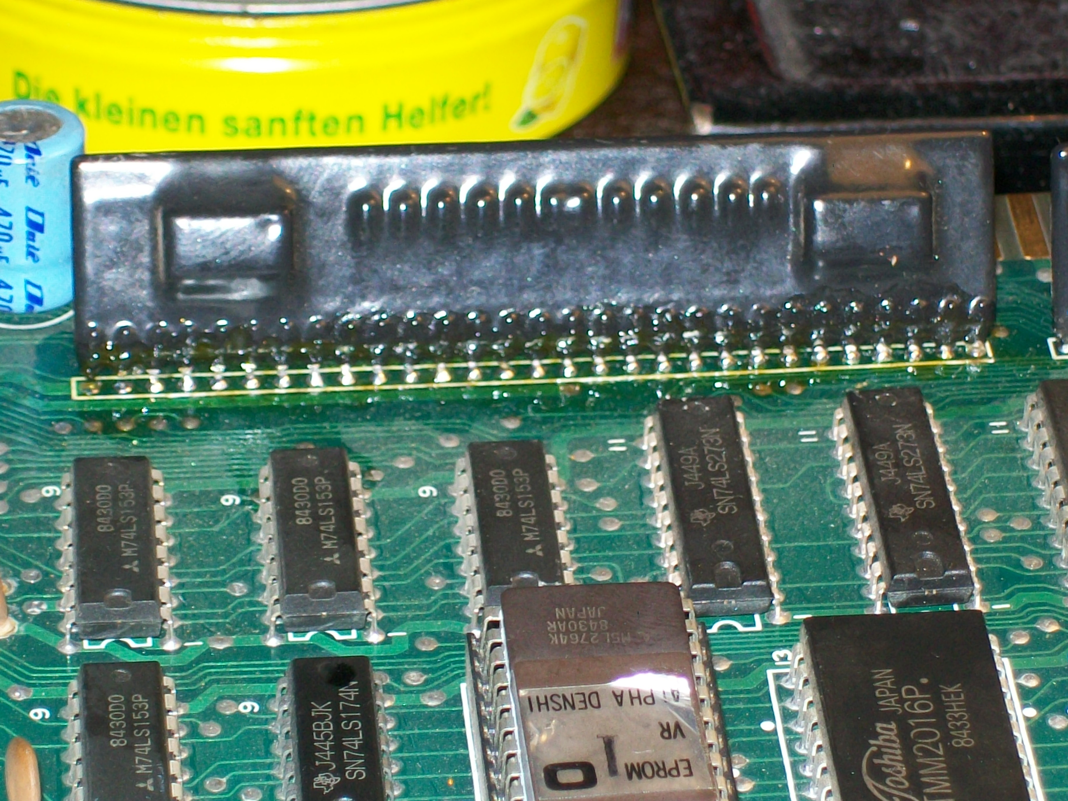
I dumped them and they were good.With my multimeter I figured out that address bus was shared among the three EPROMs while data bus was in common only among ROM 5 and 7.But I could not measure continuity between pin 15 (D3) of these two.I removed the devices from sockets and found a severed trace underneath:
PAL UpdatesComments Off on EspGaluda and Dream Soccer ’94 PAL dumps added
Oct172016
Today we have some new PLD dumps.
‘robotype’ dumped the third PLD on an EspGaluda PCB, it’s marked ‘0315’ at location U33.He also confirmed that the EspGaluda dumps of the devices @U31 and U32 work also on DoDonPachi Dai Ou Jou (both ‘vanilla’ and ‘black’ version) providing the correct labelling too.
‘frsj8112 sent in dumps from a Dream Soccer ’94 PCB (on Irem M107 hardware).
All dumps have been tested as working in a GAL16V8 targeting device.Thanks to them for the contribution.
Lastly, we found that Street Smart and Prisoners of War (P.O.W.) share the same PLDs, they are in same location since hardware is identical.
This Thunder Cross II board was stuck in a watchdog cycle.
A quick visual inspection showed this
It was easy enough to bend this back a little without causing any damage.
Powering up the game, it would sometimes show the RAM/ROM test screen from the POST with failures reported and sometimes it would just reset straight away showing nothing.
Using a logic probe I quickly found the RAM at 1H and 16E were bad both of which had completely dead output pins.
I piggy backed a known good working 6116 RAM chip on top of both of these and while it didn’t cure all my problems, on the time it booted to the test screen these RAM’s now showed clear.
I replaced them and moved onto the resetting issue.
The reset on this board is handled by a custom SIP package. I was fairly sure this wasn’t to blame as on the occasions it booted up, if I held the TEST button down to reinitialise the EEPROM the game did not reset throughout the initialisation.
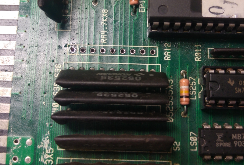
I did notice a 4.7k resistor array was missing.
I replaced this but it made no difference.
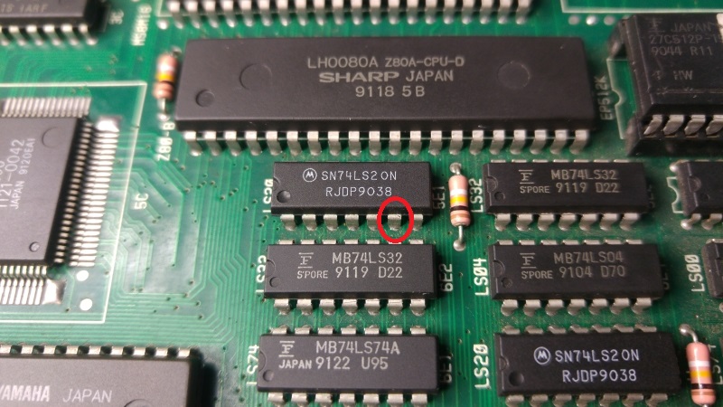
Next I noticed the game booted up more regular if my hand was on the 68000 CPU. Things like this are a good indication that there is a floating pin somewhere. Probing the CPU pins revealed that pin 21 of the 68000 (/VPA).
Chasing this proved difficult as there was a broken trace somewhere but these Konami boards have really small thin traces and vias. I eventually traced it back to pin 6 of a 74LS20 at 5E1.
Jumpering this gave me a booting game.
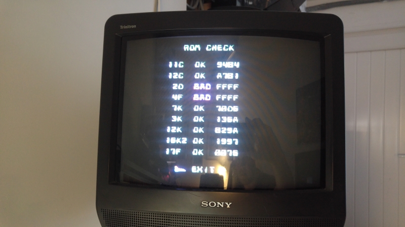
Everything initially looked good, the attract mode played and the sound effects were present. The problem came when some music played. To start with it sounded terrible but once the music stopped all the sound effects were either messed up too or were missing altogether.
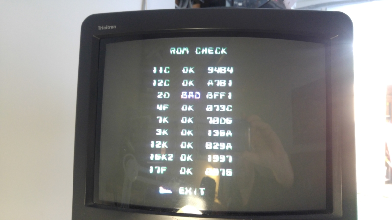
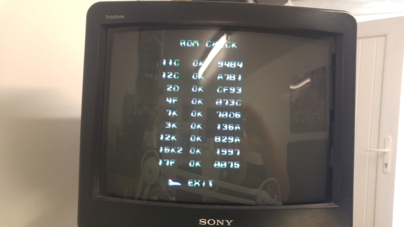
I fired up the test mode and did a ROM check which game me this
or sometimes this
I had verified the ROM which checked out OK and sound effects were present. The music also attempted to play so I was fairly sure the CPU and ROM were good.
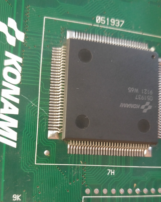
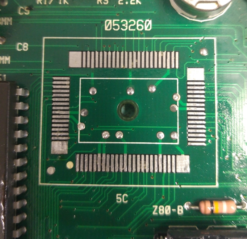
I started looking at how the MASKROM was addressed and how the PASS/FAIL data was send back to the main CPU. This all led me to the 053260 custom chip at location 5E
I mapped out all the address and data line to the MASKROM and noticed that anything after address line A10 was dead. Looks like we have a dead custom.
As it happens I found a scrap Konami PCB in the loft from which I could harvest this chip from.
Replacing this gave me my sound back and the ROM tests now all pass.