The board was faulty, most of sprites had jailbars:
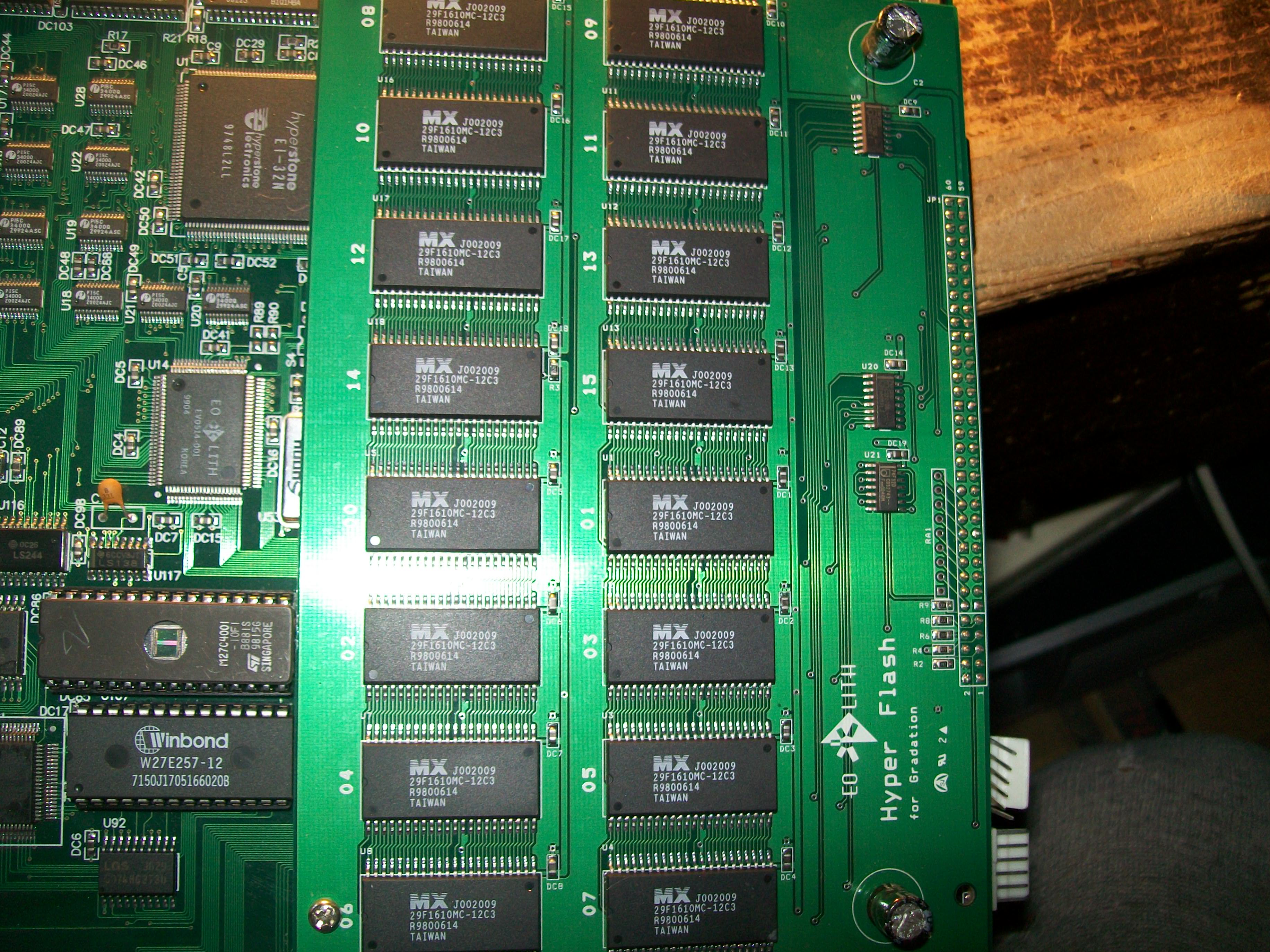
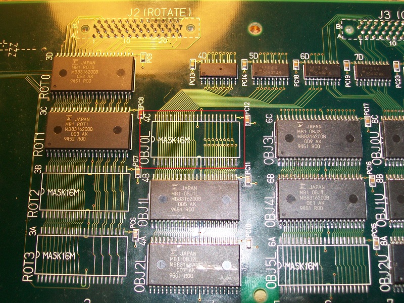
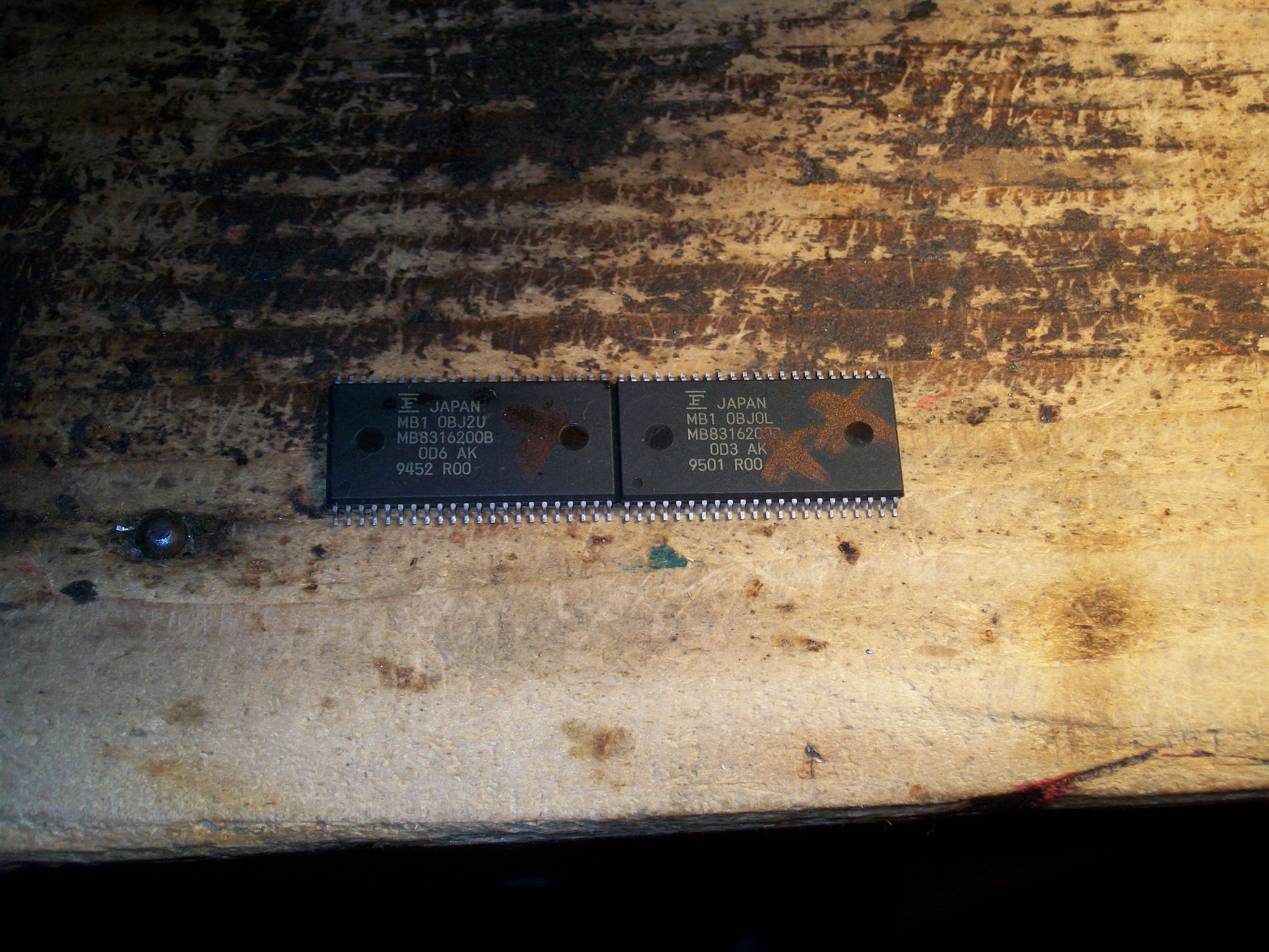
Sprites data are stored in ten 16Mbit MASK ROMs (Fujitsu MB8316200B in SOP44 package) located on the MASK ROM daughterboard:
Probing them with a scope didn’t help much since each column of devices has shared address and data busses.So I proceeded in this way.I created some empty binary files (2MByte each one) and loaded them one at a time in MAME in order to reproduce the issue and pinpoint which devices were bad.When I did it for the ones @8A-8B-8C I got pretty same artifacts under emulation:
So I went to remove these MASK ROMs starting from the one @8A of the column :
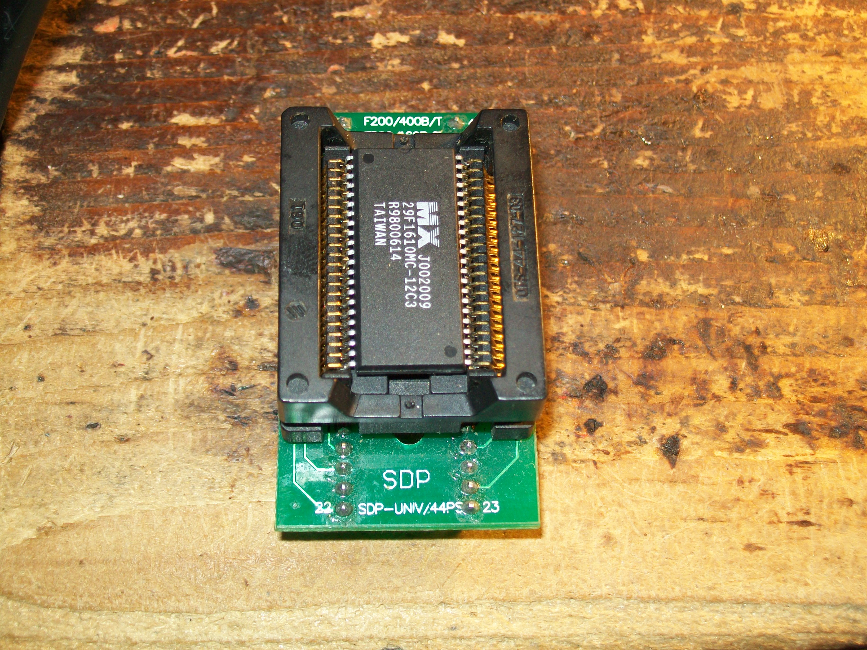
And I hit it since I was not able to get always same CRC when dumping it so device was really bad.Replacement for the MB8316200 is a Macronix MX29F1610 Flash EEPROM which has same pinout (except for pin 1 and 44 which are used for programming)
Luckily I was able to find among my spares a donor board where to take the devices from :
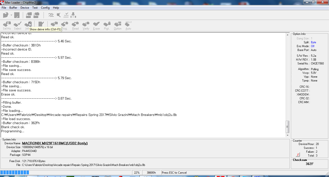
Time to program it using a SOP44 to DIP adapter:
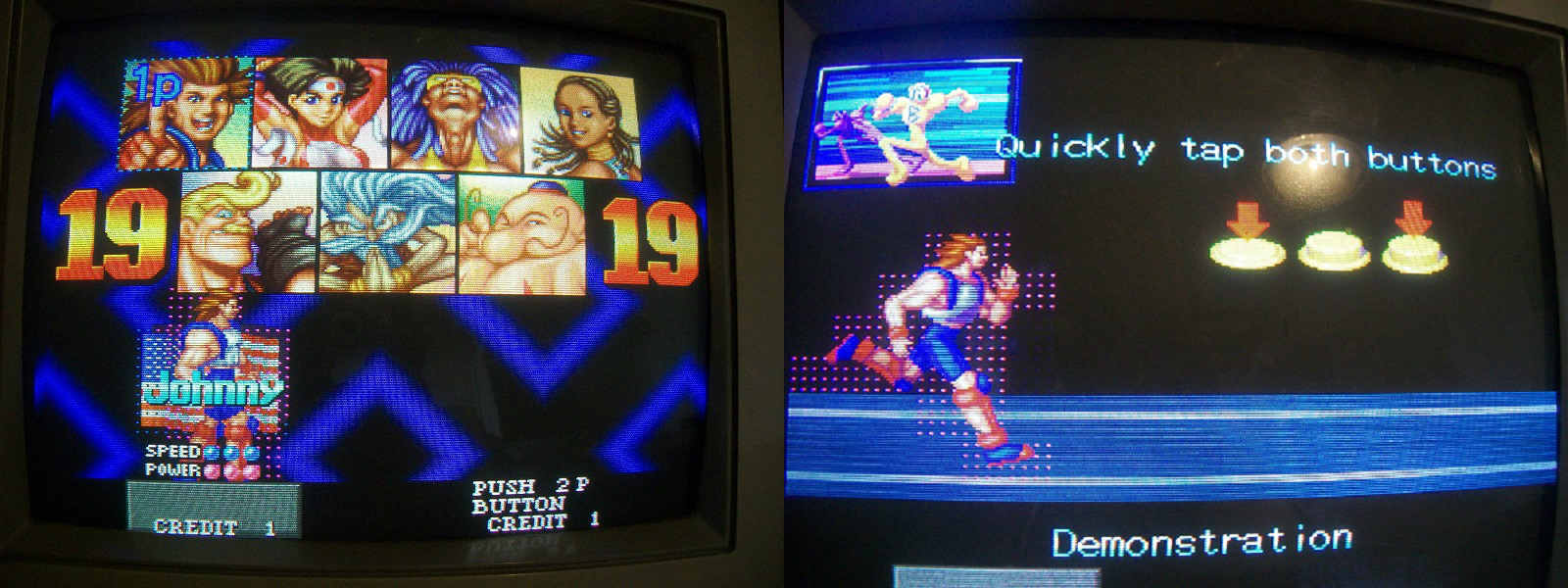
After soldered it on board I got a big improvement, jailbars were gone away but there were still dots on sprites:
Again I went to corrupt the MAME ROM files and I could pinpoint which was the involved device: the one @4C.I removed it :
I dumped it several times and obtained different CRCs at each reading, it was really bad.As further proof I loaded one of these bad dumps in MAME and I was able to reproduce exactly the issue:
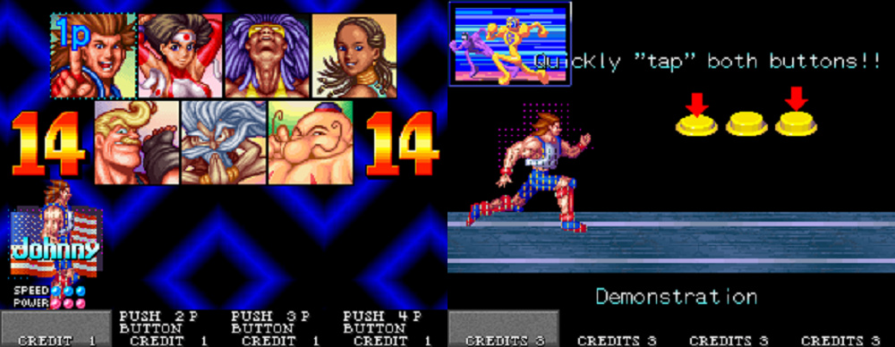
I programmed a new MX29F1610 EEPROM as replacement, this fixed completely the board:
PCB Repair LogsComments Off on Zupapa! (Neo-Geo MVS conversion) repair log
Apr202017
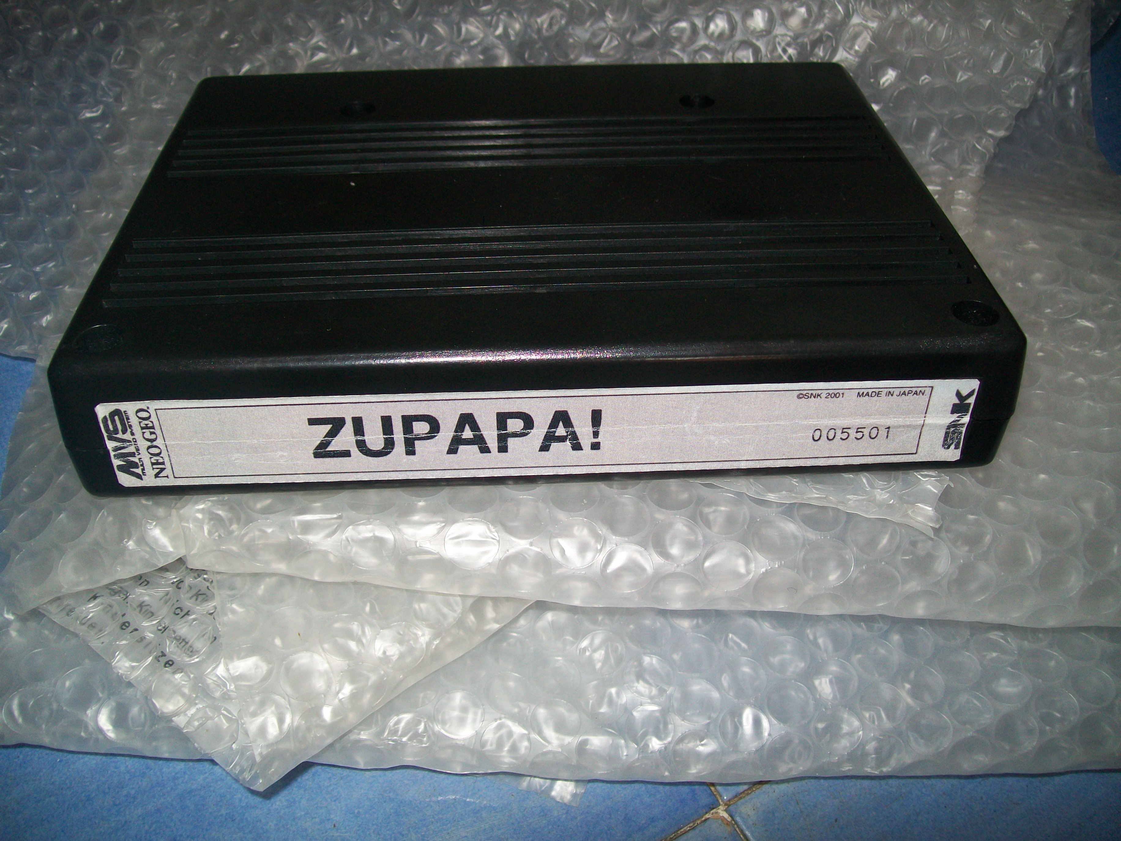
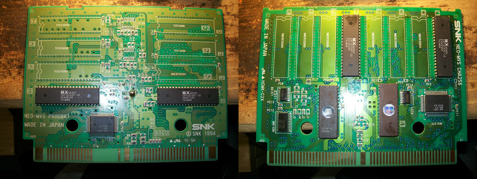
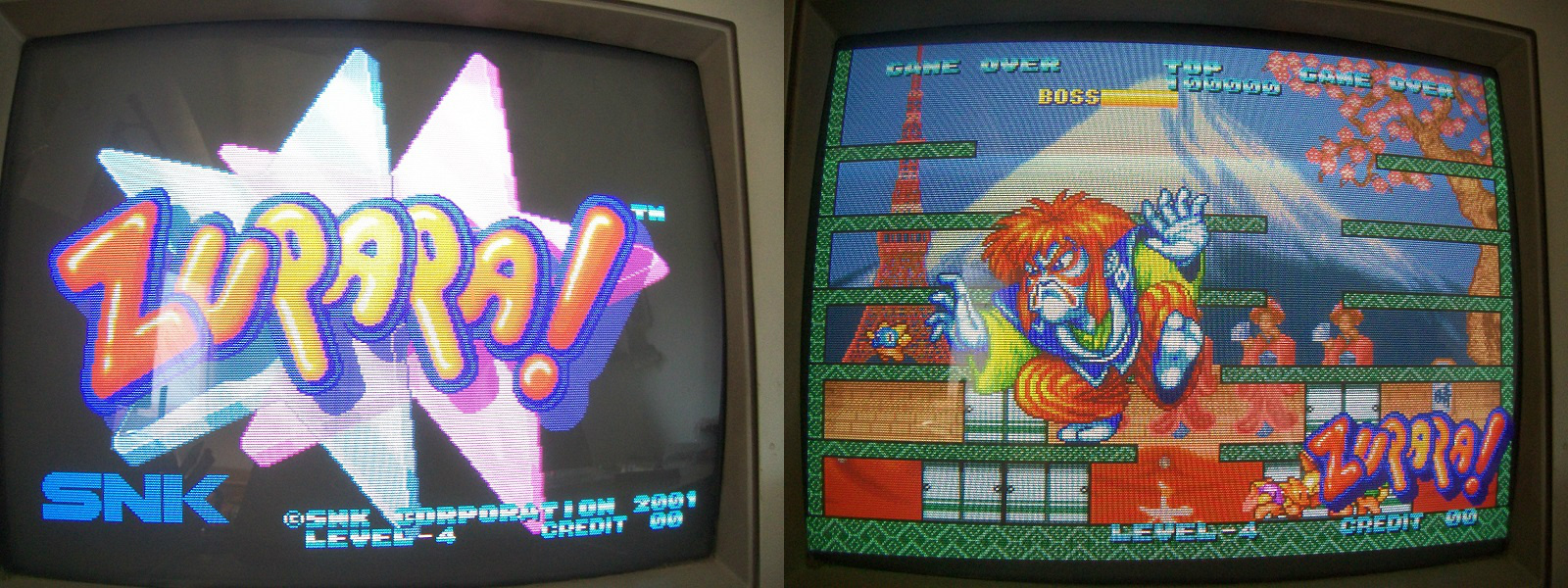
Got for repair this Neo-Geo conversion cart of Zupapa! a platform released in 1994 only for MVS system and not on the Neo-Geo AES home console :
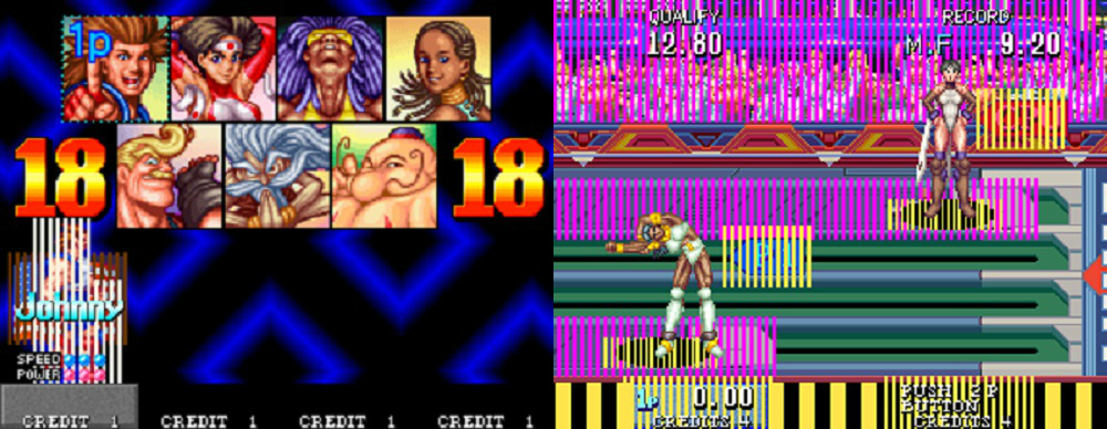
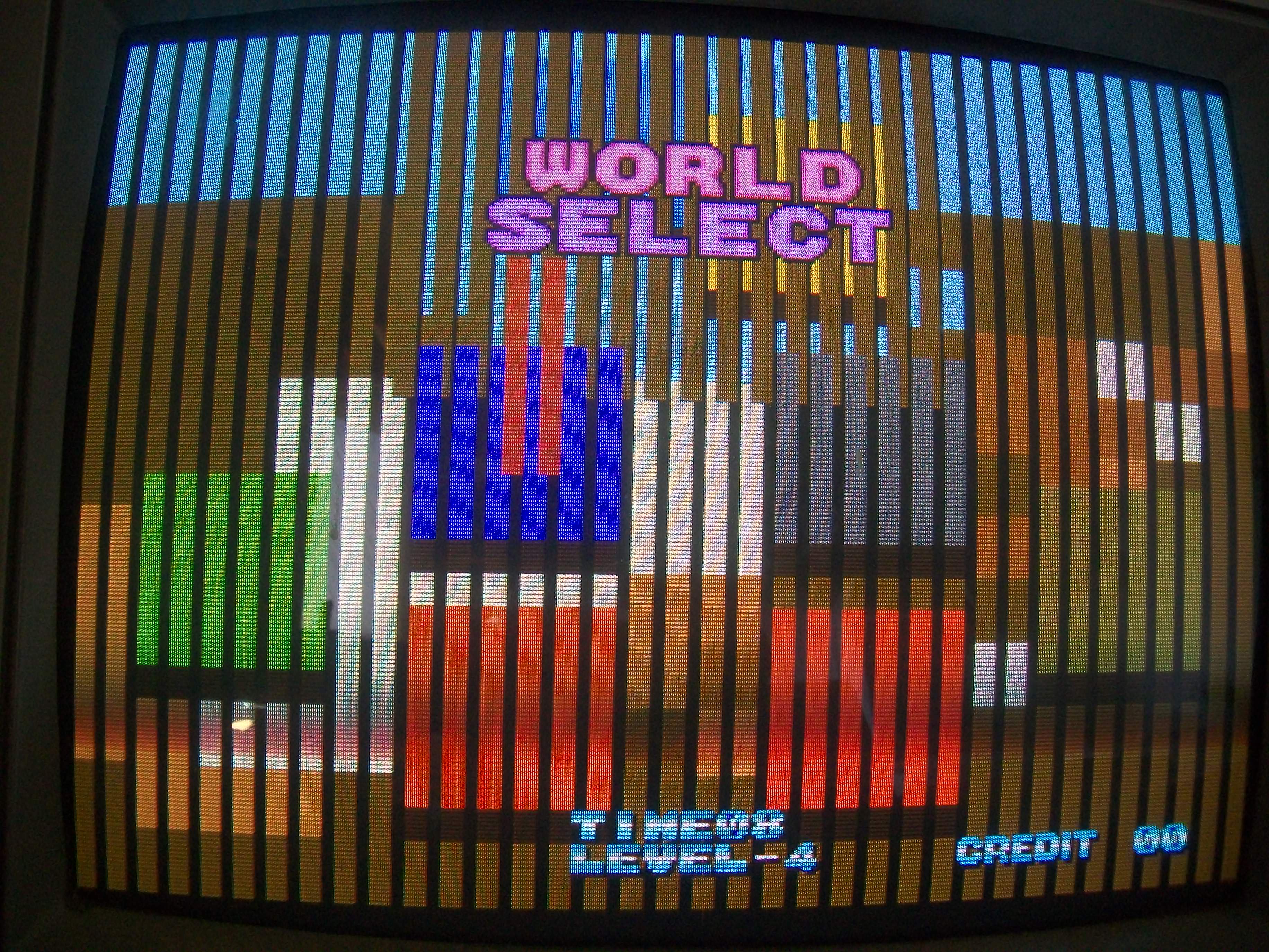
Most of graphics were blocky:
I opened the cart:
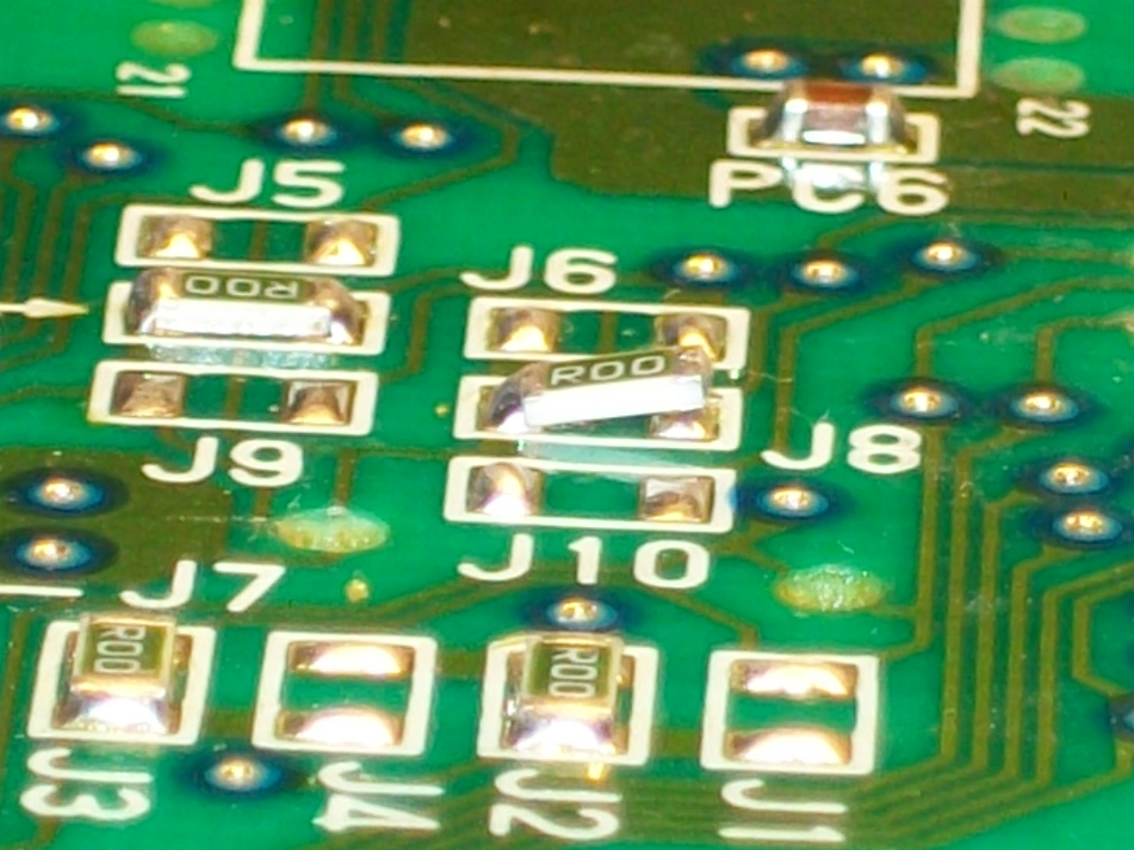
As I said, the cart was a conversion from a donor hardware, this requires the ROMs to be replaced with game code and data plus some other modifications like adding some ICs and jumpers.Doing a visual inspection on work done I found nothing of abnormal until I came across this:
One of the zero Ohm resistors used as jumper required by the conversion was badly soldered.I put it in place and magically all the graphics came back:
PCB Repair LogsComments Off on Wild West C.O.W. Boys of Moo Mesa repair log #2
Apr162017
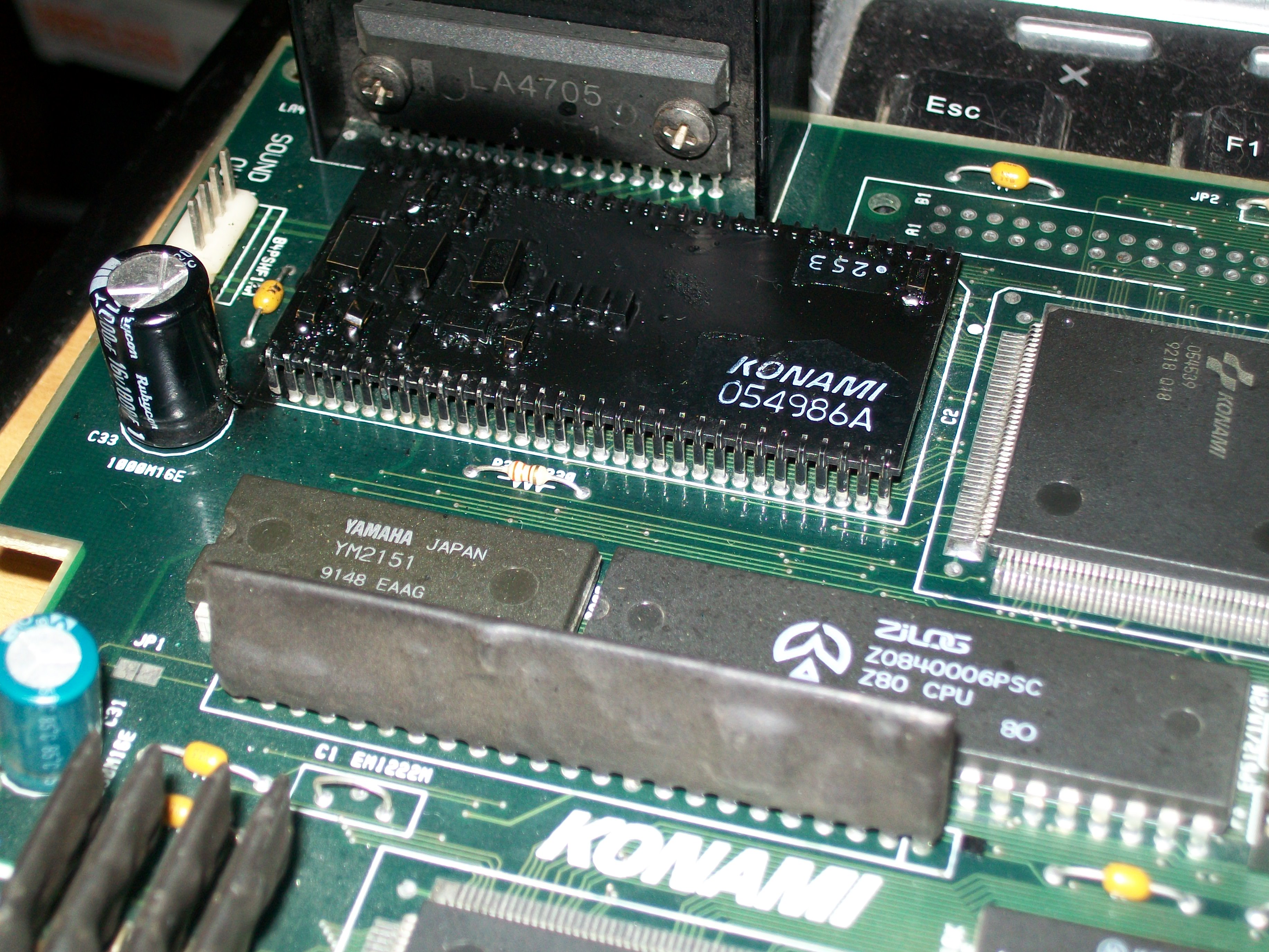
Received this Wild West C.O.W. Boys of Moo Mesa PCB for replacing electrolytic capacitors on the infamous ‘054986A’ audio module although sound was still perfectly working :
As usually I opted for tantalum capacitors, this was the final result:
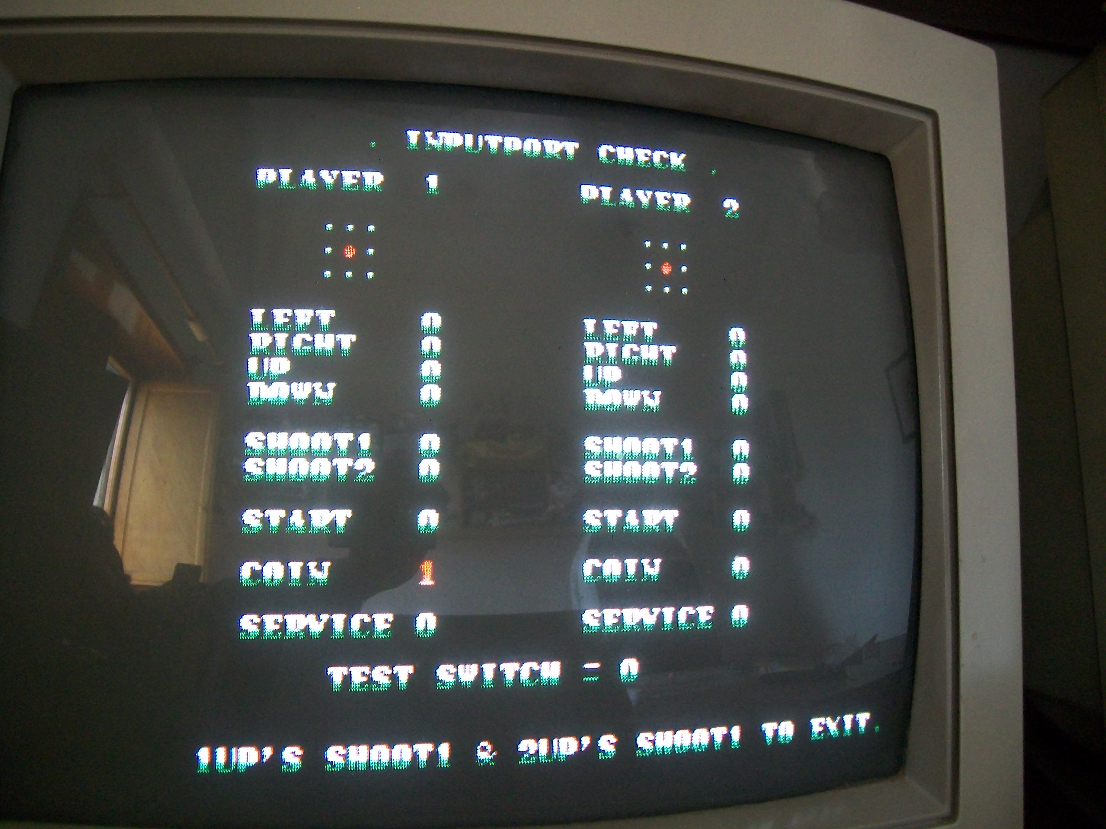
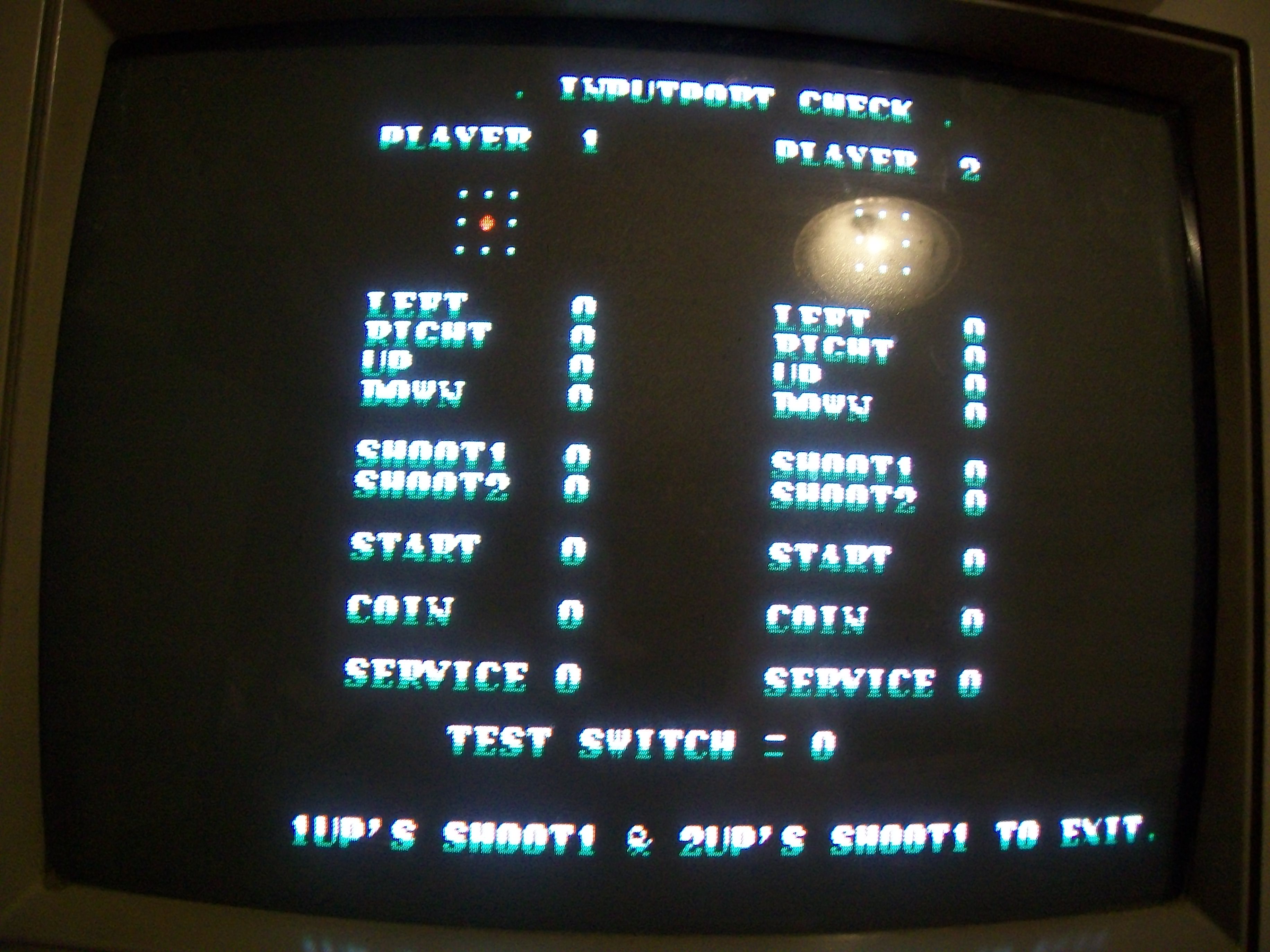
But when testing the PCB I noticed coin input of player 1 was not working, this was confirmed by I/O check which showed this input as stuck:
As workaround somebody put the game into free play:
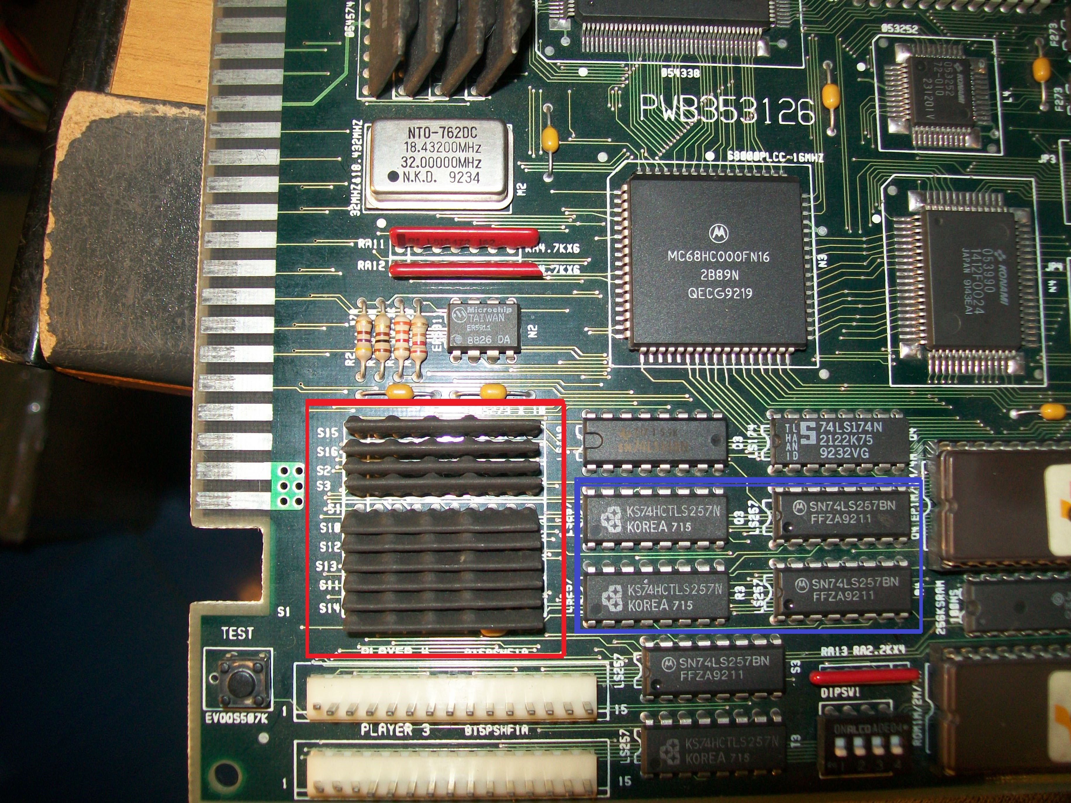
This is a common issue on the all Konami boards that share the same hardware design.The input signals from JAMMA edge are first routed to some some custom resistor arrays marked ‘005373A’ then to four 74LS257 which multiplex them :
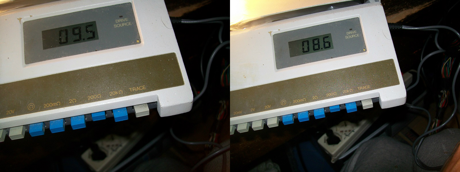
Checking the involved part revealed that input of the 74LS257 @Q3 was almost shorted to ground as well as obviously the output of the resistor array @S15 connected to it:
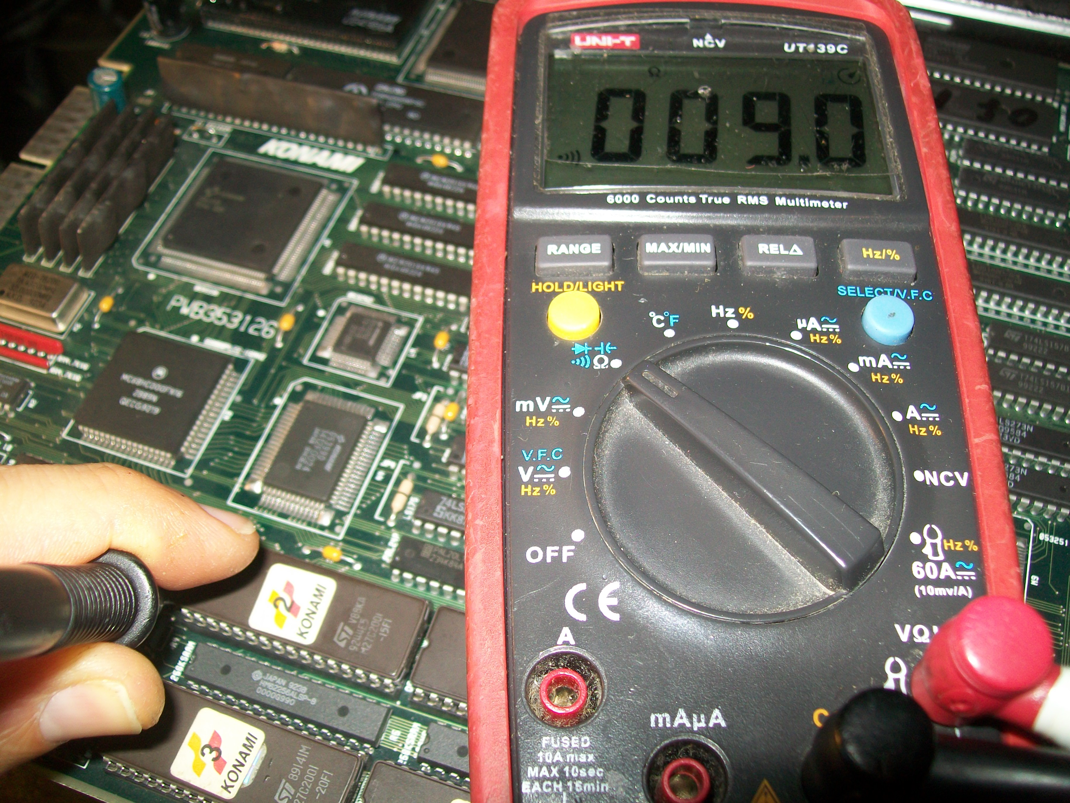
So the problem was in either of them.Using an audible milliohm meter I was able to locate the point of less resistance with ground in the 74LS257:
So confident I removed the IC:
It failed when tested out-of-circuit:
Replacing it cleared the issue, input was no more stuck.End of job.
I’ve decided to do this in two parts, the reason for this is that the faults to this board are so extensive. I am convinced that this board was hit by a bolt of lightning.
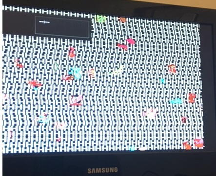
Symptoms – game booting to a screen full of zeros and watchdog barking. Z80s reset pin was also asserting but the sequence was incorrect ( just a hi flashing signal on the logic probe with no low ). There was also a perpetual low frequency sound with a higher pitched sound superimposed on top of that.
Did the usual troubleshooting. +5.15v voltage at the edge and 4.5v at the chips. Thought this was a little low. Something is dragging it down, I decide not to panic too much.
A previous repair was attempted so I decided to check all the socketed chips out of circuit first before proceeding with my own troubleshooting. Brand new components H16,E12,G17,G18 and the 74LS245 at H17 tested good. All EPROMs on the top board checked out fine with romident.
The owner of the board mentioned that the board was activating the coin meter on its own, then that eventually stopped. I take a stab at the 74LS08 at A2 which seems to drive COIN 2. My logic probe registers dead outputs on the chip and it tests bad out of circuit too. Of course changing it made no difference to how the game runs. I would soon discover that the 74ls08 seems to be a high failure Fujitsu component in this board.
Troubleshooting the z80 reset
I wanted to check out what was going on with the strange reset behavior of the Z80 reset line first.I remove D18 and test it out of circuit, sure enough it tests bad so I replace it. This fixes the reset signal and it’s now going from low to high as expected. Half the pins on the z80 are floating and the data lines aren’t toggling so I remove it and install a replacement from a parts board. The new z80 is alive although not for long before the CPU crashes and the data lines get stuck again.
At some point in the repair the Z80’s data lines stopped toggling again from an initial reset. I traced this to stuck enables on the LS138 at C18 which tested fine out of circuit but the 74LS08 at C9 feeding /G2A on C18 actually failed. Replacing C9 fixed it again. I still had stuck /OEs on both sound EPROMs but I would look at this issue later.
For some reason A16 on the bottom board caught my attention, of course this was a Fujitsu branded 74LS08 as well. I had a brand new one in my hand so I thought “what the hell” and piggy backed the new one on top of it. This seems to have cleared the screen with the initial junk. I also found another bad 74LS08 at H2 which changed nothing after replacing it.
I also found 4 additional bad chips @ F13, E15,C12 & C14 and replaced those with no obvious change.
Troubleshooting the Konami1 – watchdog / reset issue
With pin 19 barking furiously I decided to trace it’s origin thinking that perhaps there was a problem with the watchdog. Both /E and /Q clock frequencies were correct on the CPU ( 1.53Mhz ) .
I found a bad resistor at r43 ( measured 2kohms instead of 1kohm ) so I replaced it, no change.The reset signal actually originates from the bottom board .I traced and tested every chip in it’s path starting from the Konami1. ( top board [D18, B2 then the CR13 connector], bottom board [A1,G2,C4, 504 ]. G2 ( Another Fujitsu 74LS08 ) tested bad, replacing it didn’t change anything after testing. I was starting to lose confidence at this point.
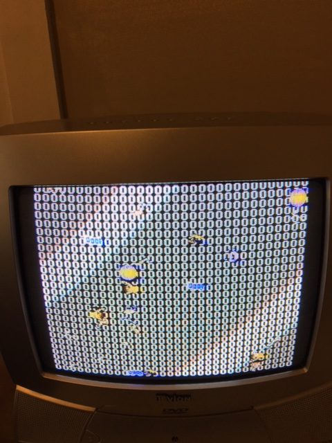
I started to probe the /OE enables to the game EPROMs and saw that every single output was stuck high right from reset. Pins 4 and 5 ( /G2A and /G2B ) of the LS138 @ H16 were floating. For y0-y7 output to go active low, the two above mentioned inputs must be low. Since pins 4 & 5 are tied together I traced this back to pin 28 output of the Konami1. I replaced the CPU temporarily with mine from my Gyruss PCB and now I was getting a screen full of Hs, This meant that the CPU was actually executing code from ROM.
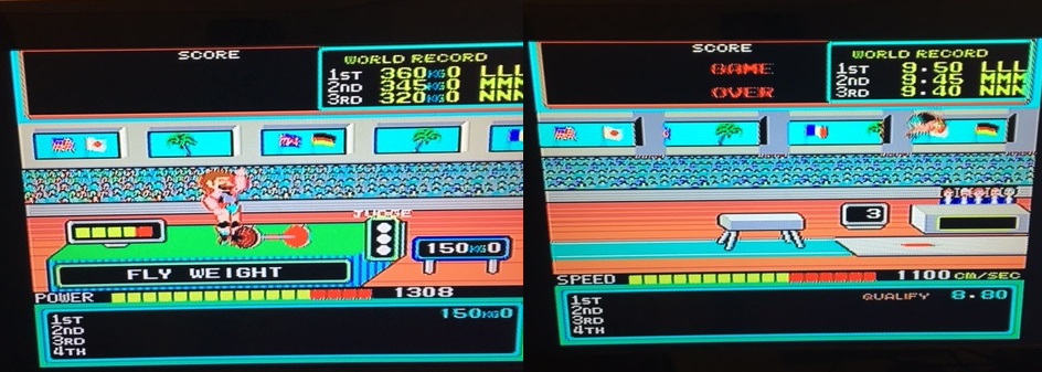
I installed the original CPU back into the PCB and measured around 1v on the inputs of pins 4 & 5 of the LS138. I would soon discover that the CPU was faulty on this line only. This CPU actually works fine in my Gyruss board [ Gyruss does not use the output of pin 28 of the Konami1 ]. So I added a 1kohm pull down resistor between pins 4,5 and ground on the LS138. This pulled the 1v down to more acceptable TTL levels and I finally got this CPU to boot to the screen full of Hs just as you see above with the good CPU. The sprite colours now seem to be showing incorrectly with red streaks compared with the last screenshot.
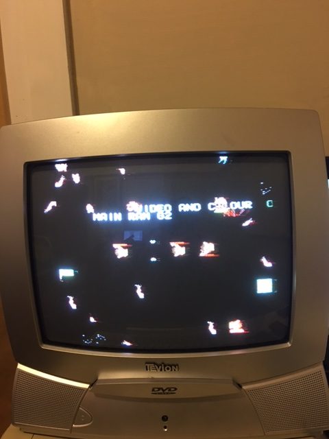
I installed my testrom into G15 which showed that the main RAM at G2 was bad.
I removed the RAM, socketed the board but the RAM tested good in my TopMax. I probed the RAM with my logic probe and saw no write enable active at all. That would do it! It seems there was a broken trace right near pin 8 of H11 when removing the chip, this was the write enable output to the main RAM. Reconnecting this line fixed the RAM error. The game was finally able to boot with the typical HS issues.
Revisiting the stuck /OE on the sound EPROMs
This ended up being bad 2114s on the top board ( C16 & C17 ). After replacing these I now had sound but unfortunately speech isn’t working. The data lines on the chip are all floating and there seems to be no clock at all. At this point it looks like a bad VLM5030 chip which I’ll have to look at later when I can get a spare.
Video issues
Replacing all four 2114s on the bottom board fixed the flickering but the colour issue still remained. I removed all bipolar PROMs and they all had the wrong checksums. So I’m going to order some and hope to fix the that also.
I’ve also decided to start using my LCD instead of the CRT which seems to have some issues displaying colours at the correct position near the edges of the screen.
After replacing the 2114 rams the Hs look a little wonky and there are some still random sprites. I’m hoping this is normal though. I’m guessing it is since the game code hasn’t had the chance to clear the object and scroll ram so it probably takes on some random values causing the wonkyness and random sprites before proper initialization takes place.
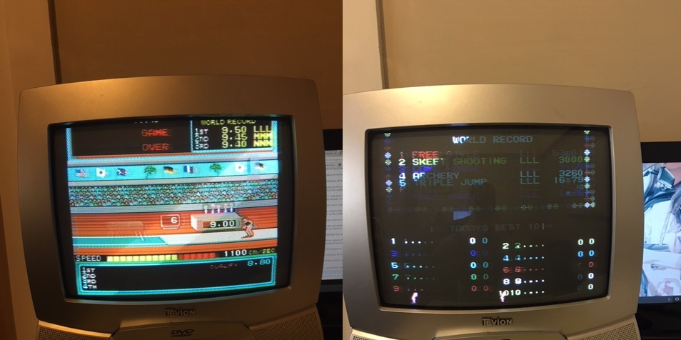
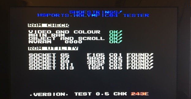
Re-working the Hypersports testrom.
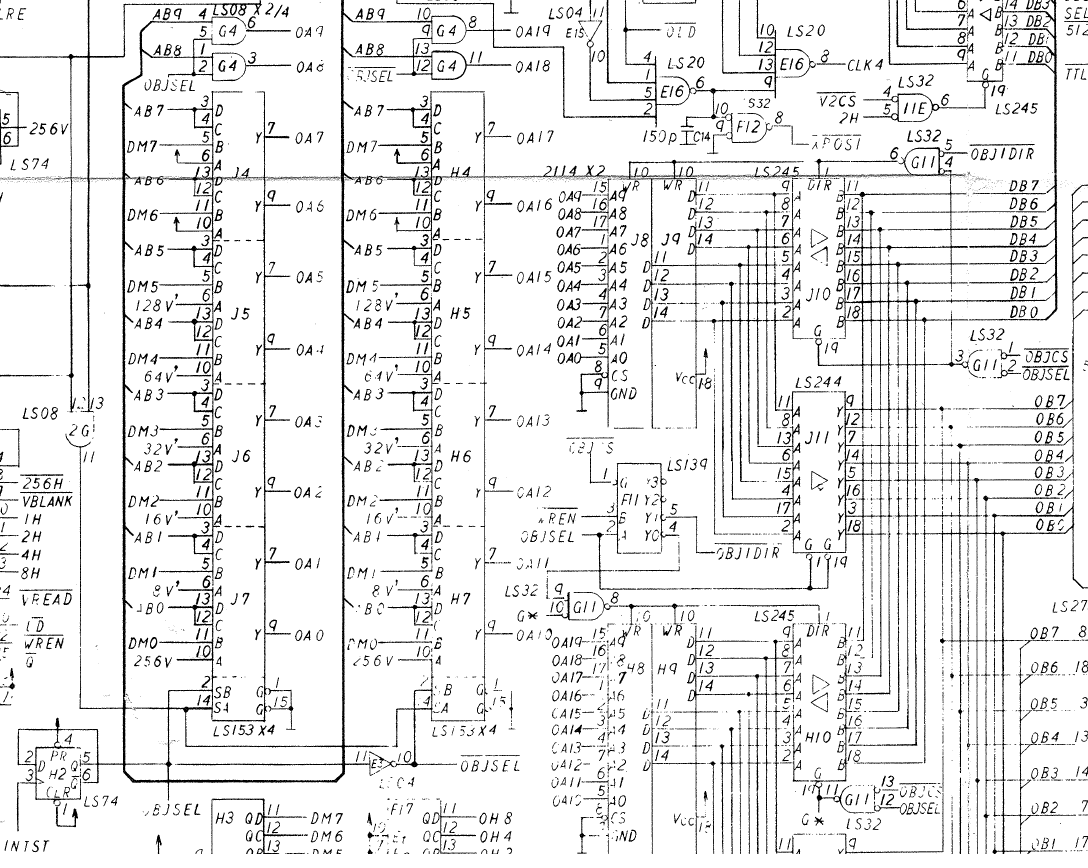
My Hypersports testrom has not been that useful at this point with the text wrapping around the screen and I should have never released it in the first place without testing it myself on real hardware. The 2114 rams on the bottom board are actually banked and occupy the same address by enabling and disabling hardware interrupts ( IRQ ). I had some trouble clearing the scroll and object RAM and it turns out I was only clearing H8 & H9. By enabling interrupts and modifying my code I was able to clear J8 & J9. I confirmed this after looking at the schematics [ the IRQ input to H2 and one of its outputs /OBJSEL ]
I wrote some code to test this and I was able to clear the screen correctly after setting up and enabling the IRQ, then writing 0s from 0x1000 – 0x13ff within the interrupt routine. The results are more than I could have hoped for.
Now all I have to do is implement the checks on J8 & J9 within my IRQ routine. Once that’s done and the necessary changes added then our runner should appear across the screen just like in T&F 🙂
PCB Repair LogsComments Off on Slap Fight (bootleg) repair log
Apr112017
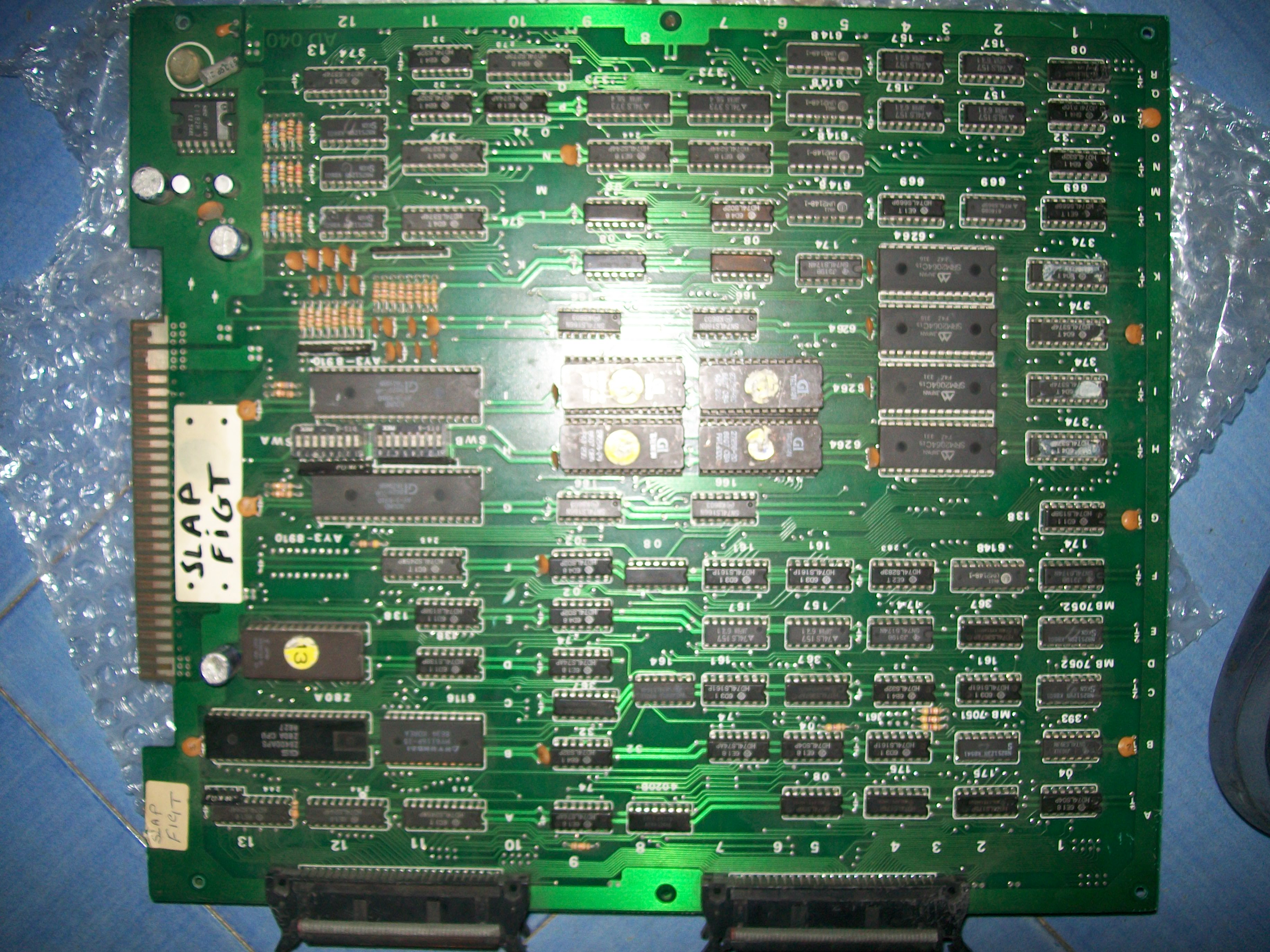
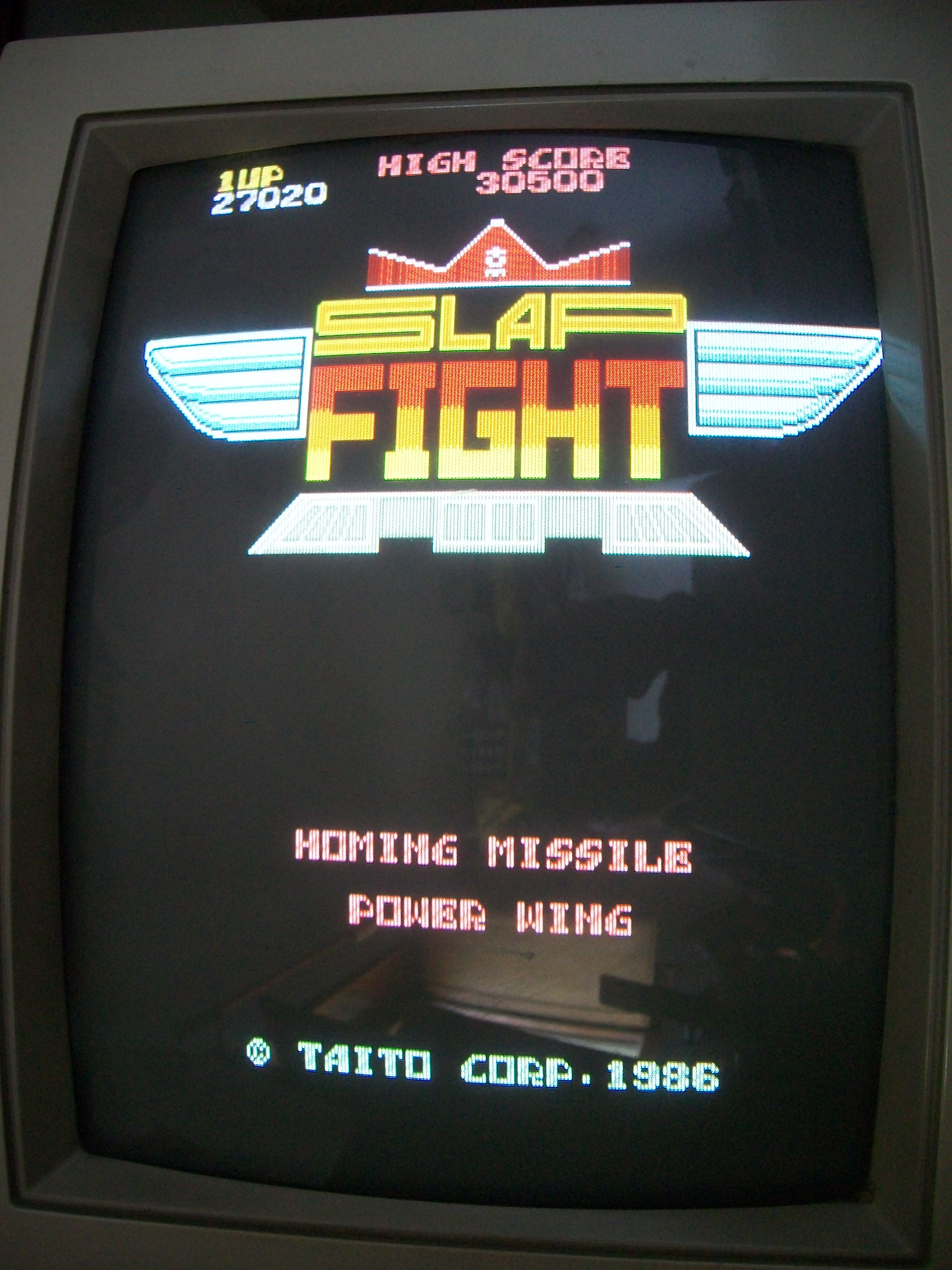
Bootlegs are worth a repair too especially when they are classic games like this copy of Slap Fight :
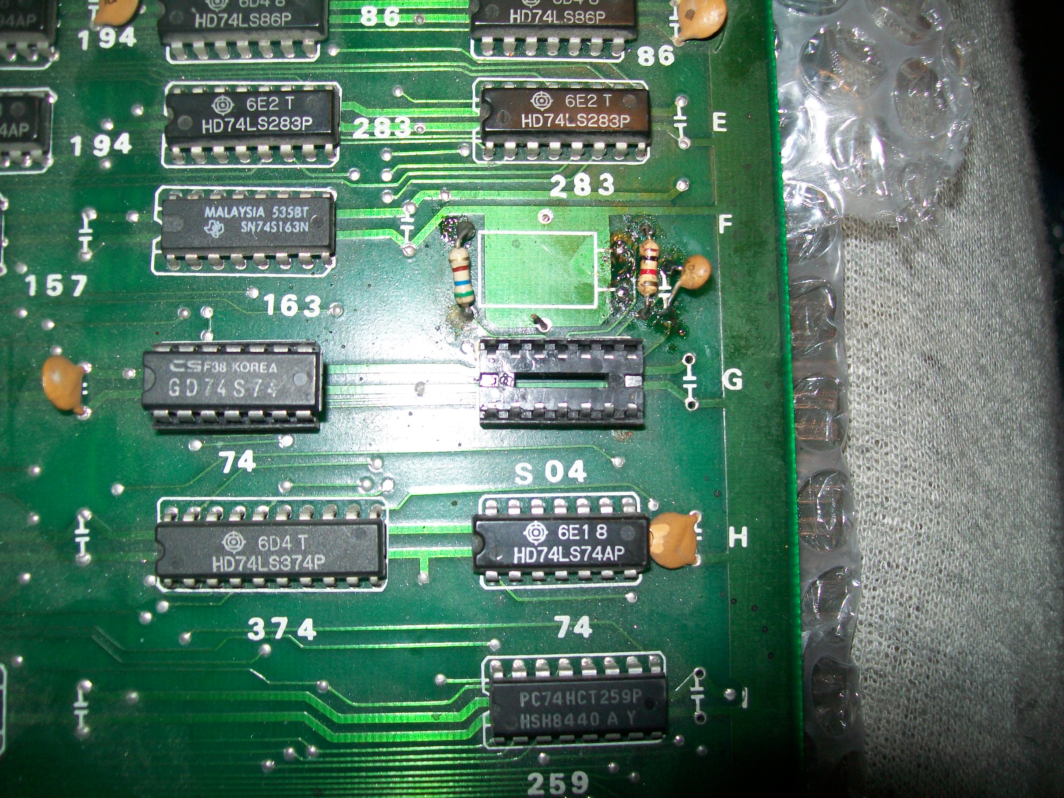
PCB was dead, no sign of activity.At a closer inspection, the main crystal which generates the master clock and the 74S04 inverter were missing from video board:
There are several bootlegs of Slap Fight and each one has a different layout and design but looking at online pictures mine was identical to original board.MAME source told me the exact value of the missing quartz :
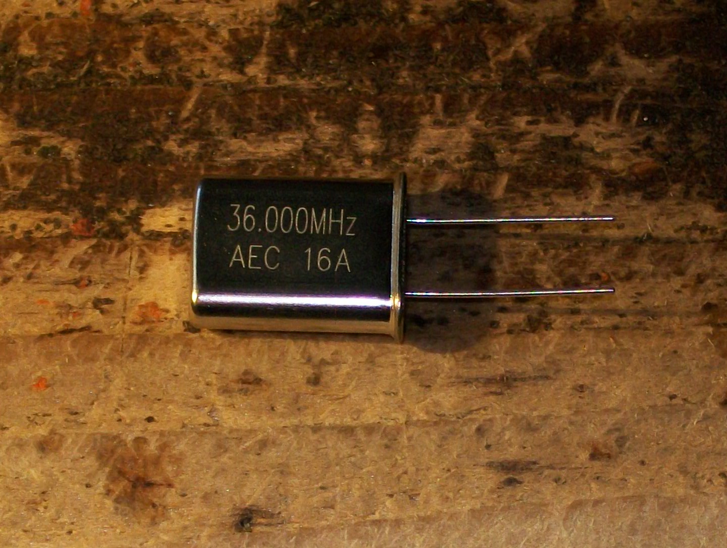
I was not able to find a 36MHz quartz among my spares (it’s not a common value) so had to order it.I got it in few days:
With the correct clock the PCB sprang to life :
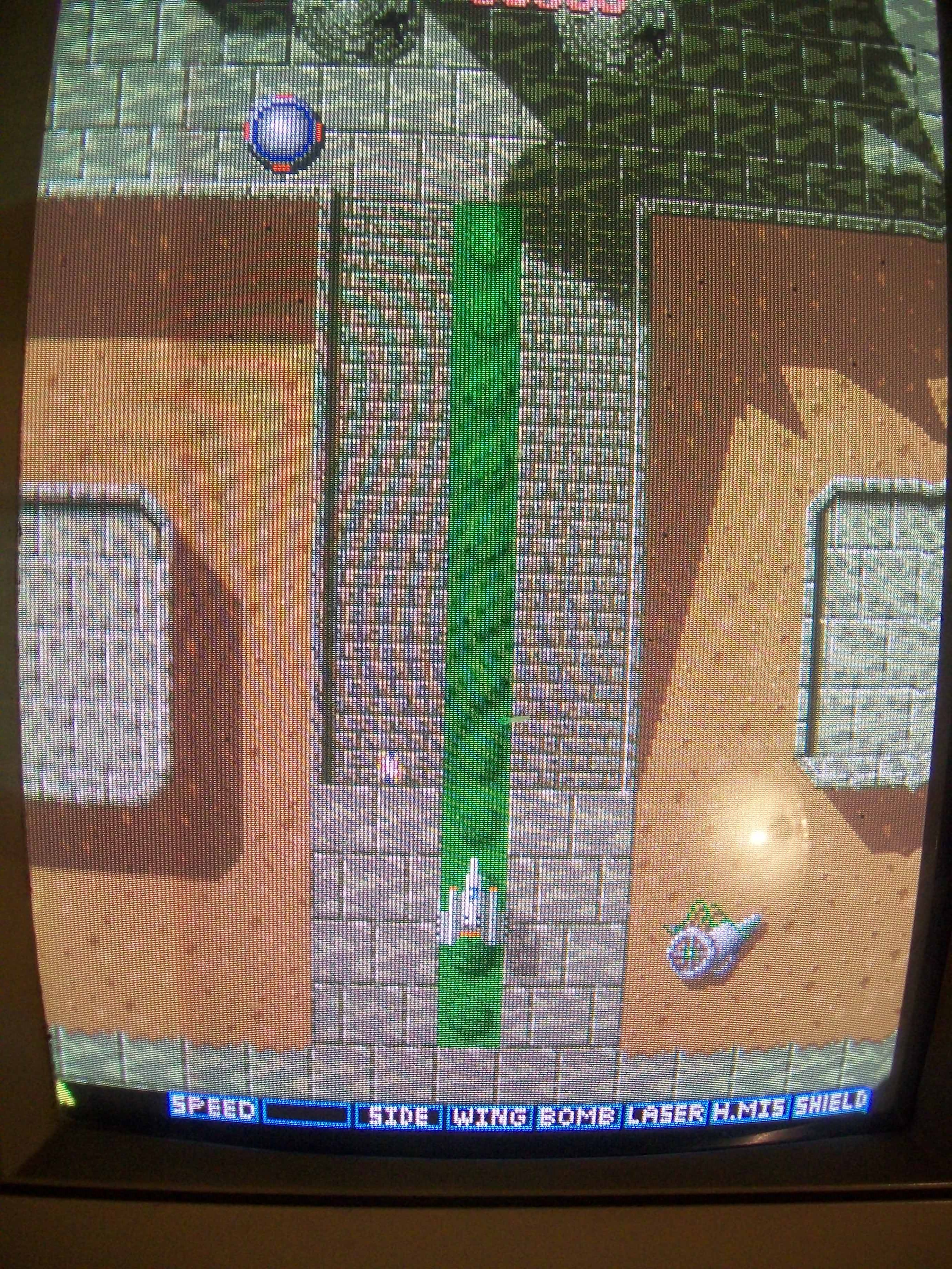
Game was playable but sprites and sound were missing at all:
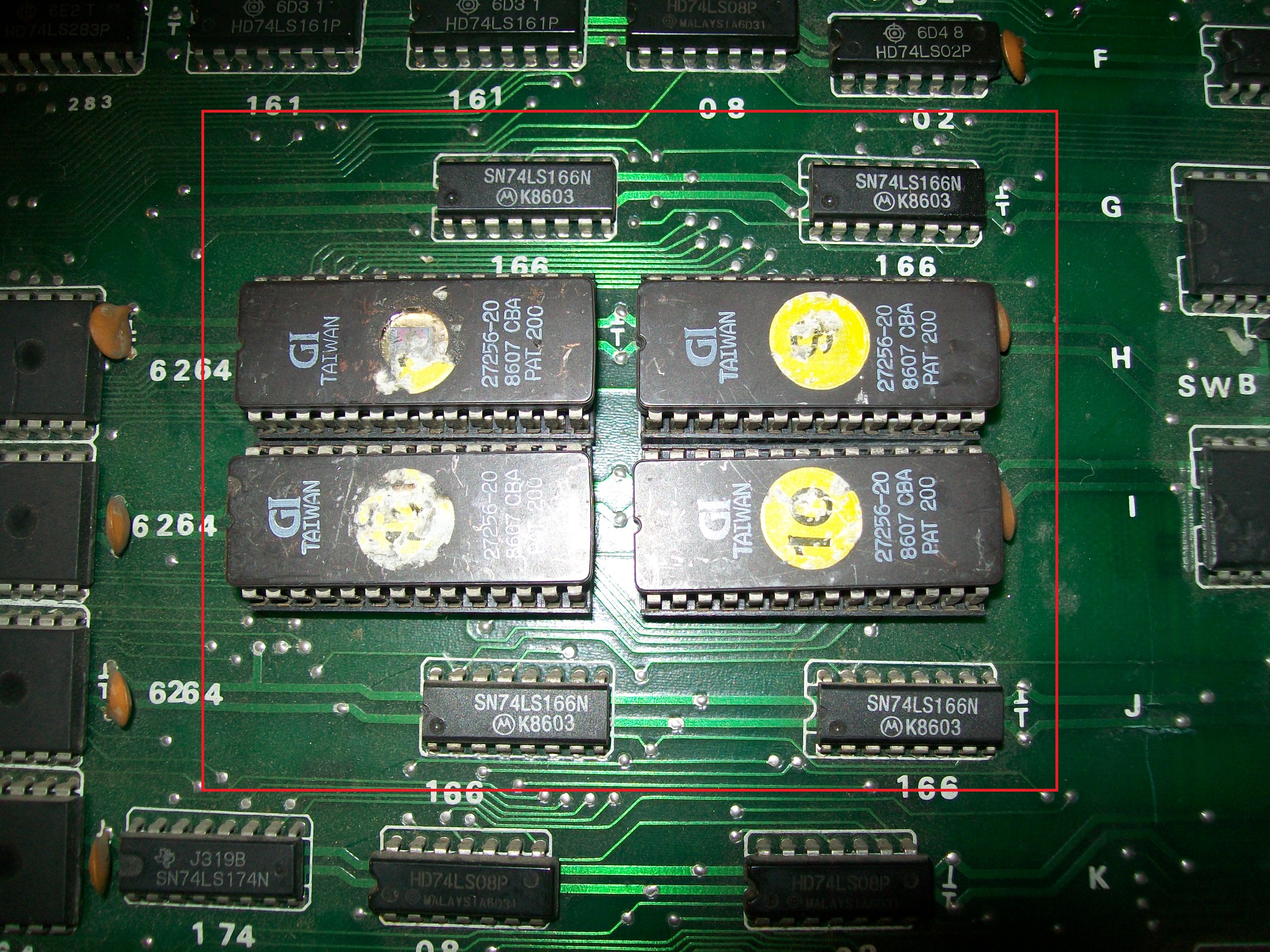
Sprites data are stored in four 27256 located on CPU board.Data lines of these EPROMs are tied to the inputs of four 74LS166 8-bit shift registers:
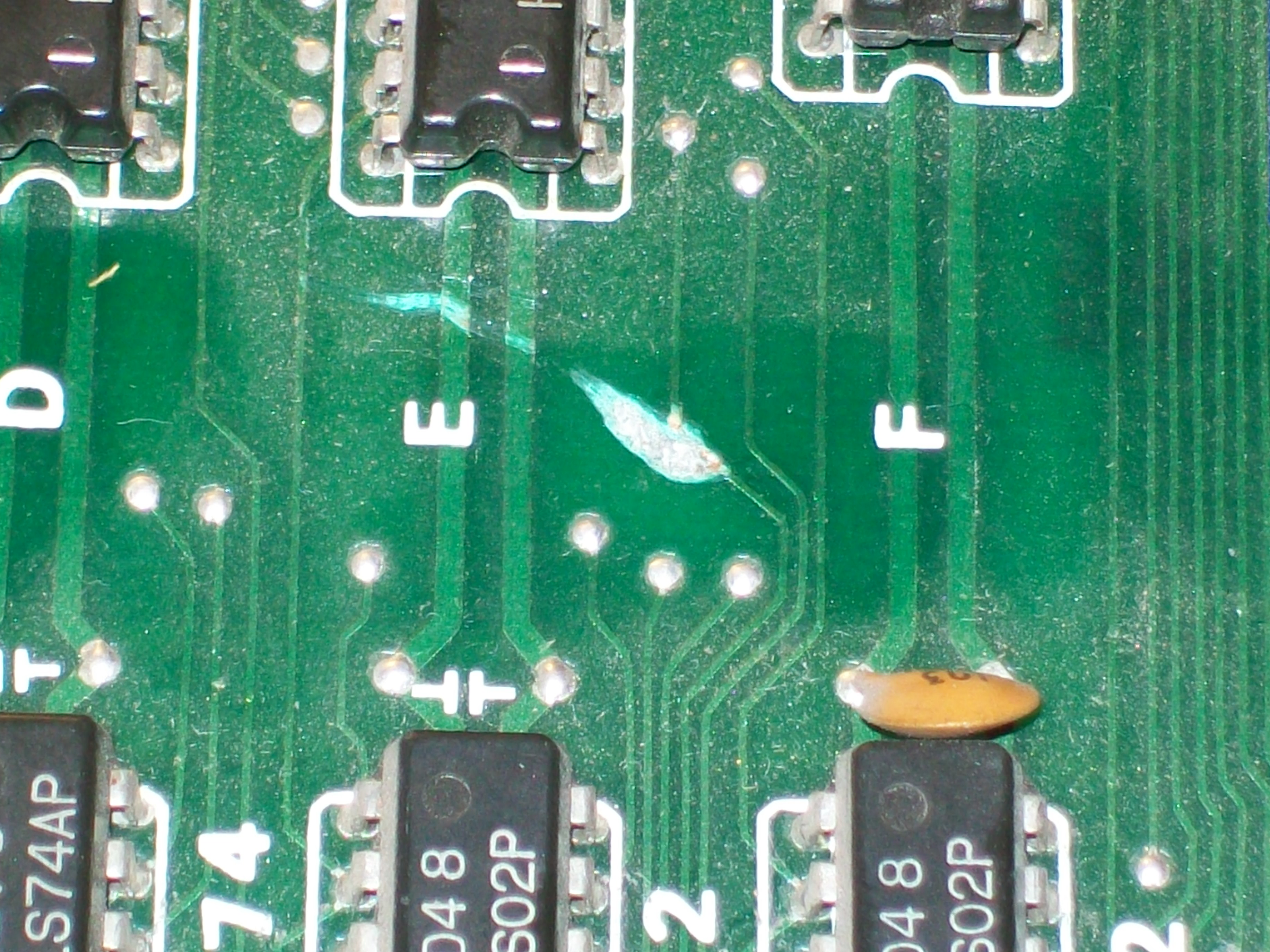
Probing the components of this circuit I found that the shift load input (pin 15) in common of the four 74LS166 was stuck high.I traced it back to an output (pin 8) of a 74LS32 whose input pin 9 was stuck too.Tracing this back lead me to the cause of the issue:
Patching the severed trace restored the sprites:
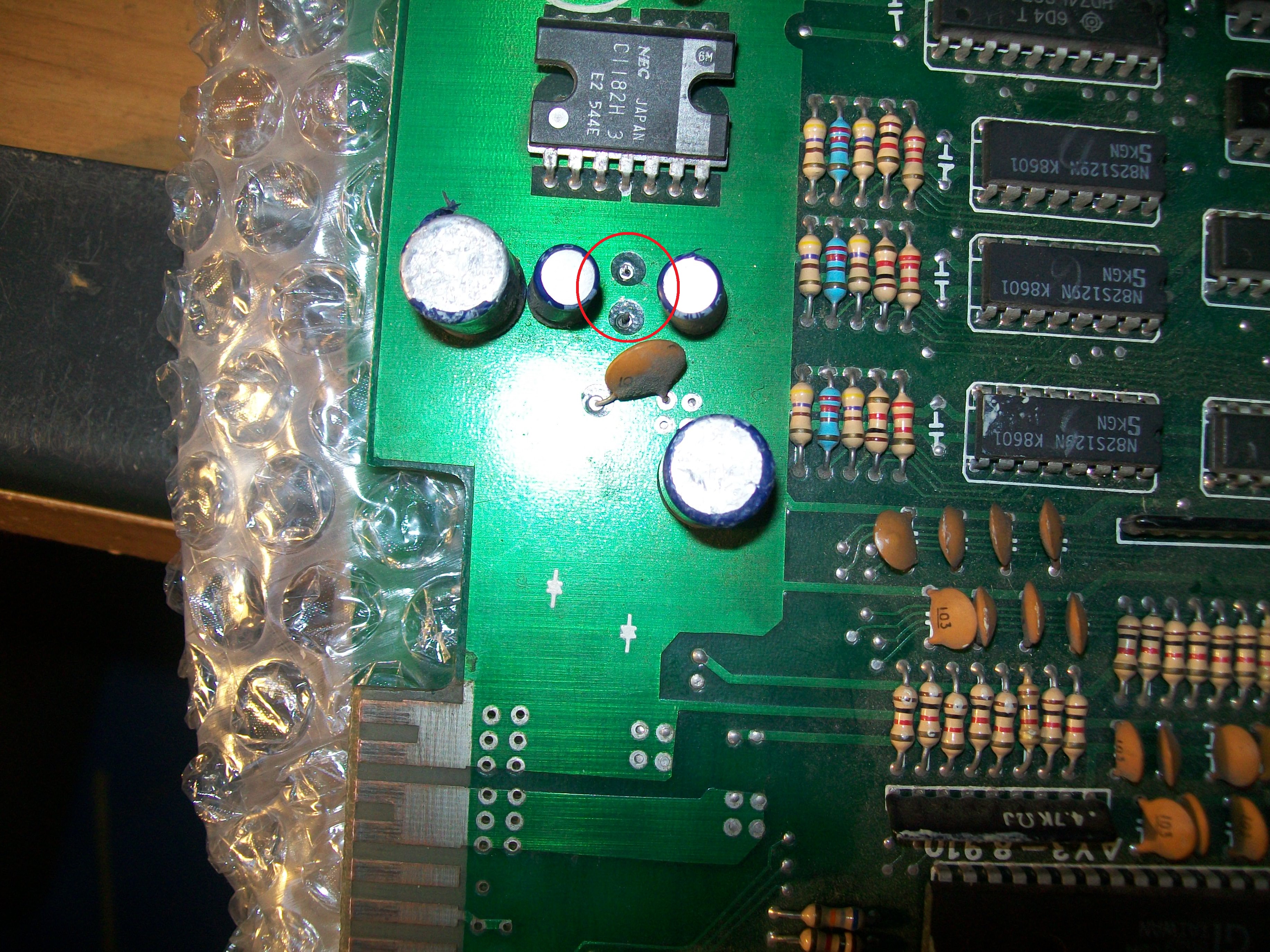
Now the lack of sound.”Listening” with my audio probe the output (pin 5) of the uPC1182 amplifier revealed that sound was present but for some reason it didn’t reach pin 10 partside of the JAMMA edge.A closer inspection revealed a missing electrolytic capacitor (used to filter the output of the amplifier)
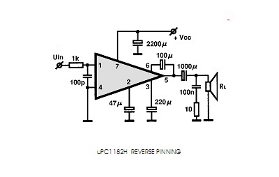
I fitted a 1000 uF capacitor as suggested by the typical application circuit of the uPC1182 amplifier:


 Patching the severed trace restored the sprites: