Oct 142018
 

Some time ago I bought an untested Sega Dreamcast console (with no video cable or other accessories included) with the intention someday to replace the optical drive with a GDEMU :

I was lucky because it was a japanese HKT-3000 model with VA1 motherboard and 3.3V GD-ROM assembly so perfectly compatible with Deunan’s GDEMU :


Some days ago I finally got an A/V cable so it was time to power up the console for the first time.With my disappoint all I got was a disturbed video signal, nothing came up on the screen:

I opened the console and did an inspection :

First of all I looked at PSU and immediately my attention was caught by the big 100uF 200V electrolytic capacitor @C3 which was clearly ‘bulging’ (you can see how top of the metal can is dilated)

This capacitor has a very important function as it filters (suppressing the ripple) the AC source that then get transformed by the rest of the PSU circuit.It measured little more than 7000 pF (0,007 µF) when tested out-of-circuit showing no ESR value at all :

I replaced it with a low-ESR one and checked in circuit the ESR of the other electrolytic capacitors, they were all good:

I powered up the console and I was delighted by the startup intro animation (sorry for B/W picture but my Philips CM8833-II monitor doesn’t accept NTSC signals)

Now waiting for a joypad and then time to play with wonderful Deunan’s GDEMU ODE!

 Posted by at 10:08 am

Silent Dragon repair log #2

 PCB Repair Logs  Comments Off on Silent Dragon repair log #2
Oct 122018
 

Received today this Silent Dragon PCB (a not so well known beat ’em up manufactured by Taito) that I bought as faulty :

According to the seller board played fine but sound was absent.He was right:

Some one tried to replace invain the audio amplifier:

A quick check with my audio probe revealed the issue had a digital and not analog cause.So I went to probe the Z80 audio CPU and found its /INT line always asserted:

This means a maskable interrupt to the CPU was triggered by an external I/O device.This causes execution to jump to a specific interrupt vector (which is some code at a fixed location).Execution  can then continue after the interrupt vector routine has finished but in my case the /INT line was LOW all the time so the CPU was not properly running.

A further check  revealed pin 21 /RD and pin 22 /WR were shorted each other:

I turned the board over and did a visual inspection on solder side, my attention was caught by this particular:

Under a microscope:

A solder bridge was shorting two vias connected not only to pin 21 and 22 of the Z80 but also to two pins of the ‘TC0140SYT’ ASIC (the sound and interrupt controller)

I removed the bridge with my iron tip and sound was back.Job done

 Posted by at 5:24 pm

Hellfire repair log #3

 PCB Repair Logs  Comments Off on Hellfire repair log #3
Oct 102018
 

Another shoot’em up ‘under surgery’.Here we have an Hellfire PCB I received from Portugal:

Board booted into game but sprites were all blocky:

Looking at hardware I could figured out the the parallel data from the four 1Mbit MASK ROMs of sprites are converted into serial by four 74LS166 8-BIT shift registers (one for each ROM)

Probing the 74LS166 @5F revealed the output (pin 13) was stuck high :

While the inputs were active:

I removed the IC:

It failed the out-of-circuit testing :

This lead to an improvement  but still not perfect as sprites were missing lines :


Looking again at hardware I could figure out the sprite line buffer is made by eight 2149 SRAMs (1K x 4-bit devices, pin to pin compatible with 2114/2148)

The one @6K was hot to the touch, probing it with a scope revealed weak signals on data lines :

Ther RAM chip failed when tested out-of-circuit :

 This fixed sprites completely:

The last issue concerned the sound, it was faint and corrupted:

Looking at sound circuit I noticed a Nec uPC1181H amplifer was fitted in place of the Fujitsu MB3730 that silkscreening suggests :

Although the two amplifiers have pretty same pinout, different is the typical application circuit and power output (14W for the MB3730 and 9.2W for the uPC1181H) so I installed a proper one.Looking at sound section on another same board I noticed three mylar 100nF capacitors were used by factory @C61-C62-C63:

Whereas on my PCB an electrolytic capacitor was installed @C61 and the one @C62 was missing :

I restored the factory condition gaining a loud and crisp sound again.Repair accomplished.

 Posted by at 10:06 pm

Kicker (Shao-lin’s road) (bootleg) repair log

 PCB Repair Logs  Comments Off on Kicker (Shao-lin’s road) (bootleg) repair log
Oct 072018
 

Earlier this year I attended a meetup at UKVAC user Bonehead’s house.
One of the things I brought back with me was an unknown bootleg PCB that a was being given away.
I opted to take this particular PCB because it was 6809 based and I needed something to help me continue work on my Fluke 90 PC software that I started quite some time ago.

This PCB uses the Konami Classic pinout for which I already have an adapter for so following a quick visual check I plugged this in and powered up.

As you can see we have watchdogging going on.
Right next to the 6809 there are two 74LS244 buffer IC’s. A quick continuity check showed that these were connected to the address pins of the 6809.

Probing the 244 at E8 showed that all the outputs were dead. Removing this revealed a broken trace.

At some point in its life there has been a sort here.
I patched the break and fitted a socket and new 244 buffer and checked for shorts before retesting.

Powered up and all was well again.

Confirmed later that the sound is present too and controls are all working.
A quick fix this time.

 Posted by at 5:55 pm
Oct 052018
 

Another PCB which has been collecting dust on a pile. I got myself motivated to repair it.

Symptoms

The PCB will not boot, all you see is a white screen.

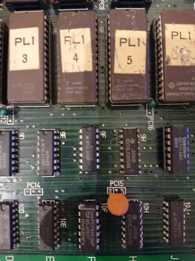
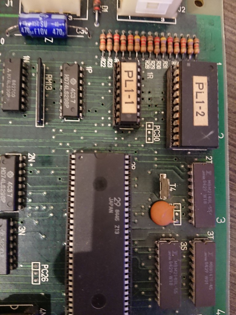
Decided to check the clock circuit first to ensure the CPU was running, it was, so clock circuit is fine. Next I checked the CPU ROMs, and found a bad ROM at location 8N. Burned a new ROM and inserted it, now game is booting but with issues.

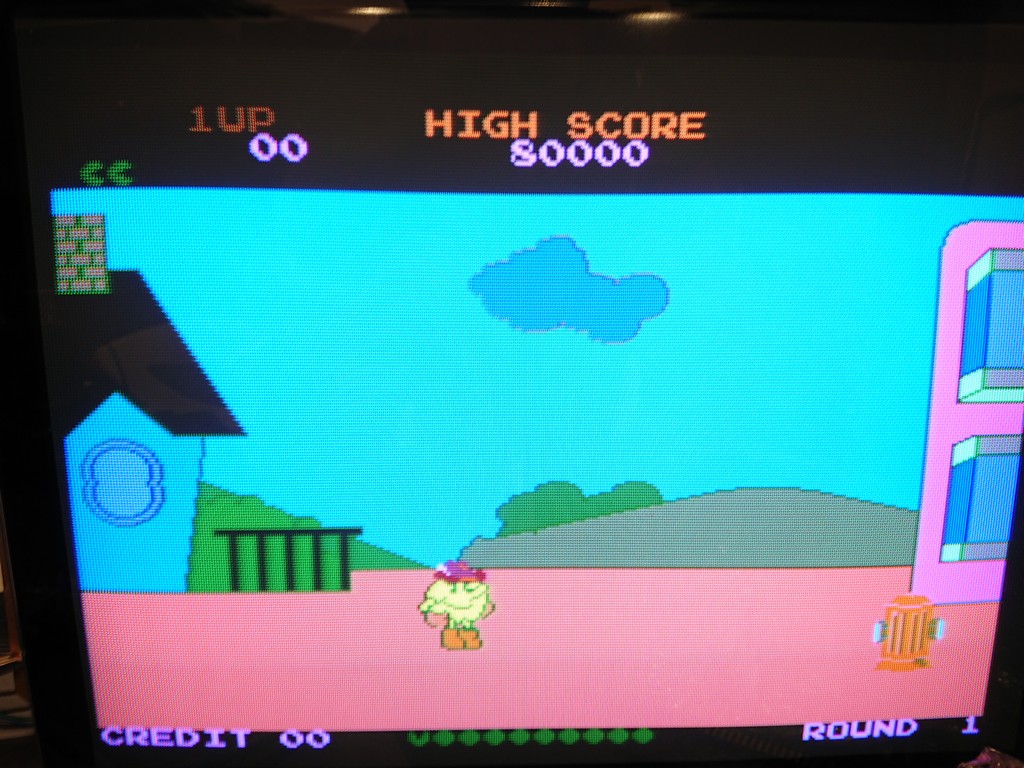
There were absolutely no sprites, and I could not coin the PCB up to start either. The background was full of jail bars.

I first checked the sprite PROM on the A board at 2E, if this goes bad the sprites will dissapear. Both the PROM and socket checked out good. So, my attention turned to the lower B board as this handles all the sprite processing.

It is interesting to note that GnG PCB will boot without the B board but without sprites of course. Handy for troubleshooting.

These Capcom PCBs have all the copper path traces masked, obviously an attempt to stop the bootleggers. Luckily, schemes are available, and they are sectioned off into relevant areas of the PCB which is nice.

My attention turned to the B board to get the sprites back up. Found a LS139 Decoder IC on the B board at 9K which for some reason was plagued with rust, I checked it and found that it was completely dead, the rust must have worked its way up.

Socketed and replaced it and now we have some sprites which are all wrong, but at least we have sprites.

Looked around the graphics ROM addressing circuit and eventually found a LS194 Decoder on board B at location 4C with pins 13 and 14 stuck high.

Socketed and replaced and now the jailbars have gone.

Whilst I was troubleshooting, I noticed that the RED had completely failed and I was left with just BLUE and GREEN, nice! I checked the supergun setup, but no it was the PCB which had failed.

I carried on looking at the sprite circuits and found a LS273 Octal Flip-Flop which had completely failed.

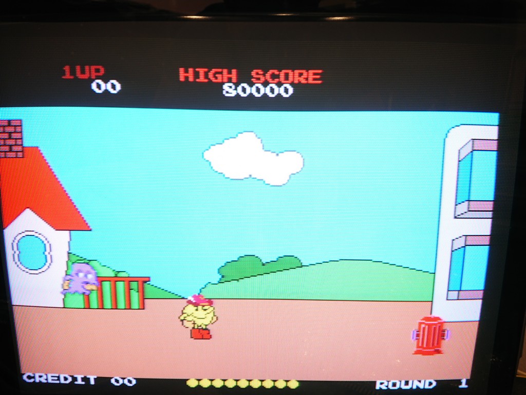
Socketed and replaced it, we now have all the sprites back!

I flipped the PCB over to look at the A board, and using the schemes I could see that a LS367 Hex Bus at location 6C was the final stage for the RED output. I checked it and found that pin 11 was stuck High.

Socketed and replaced it and the RED came back!

Finally, had to resolve the issue of the PCB not coining up. The coin up function works in the same was as the game inputs, so I knew I was looking for another LS367 Hex Bus on the A board. I checked the schemes again and it told me the LS367 Hex Bus at location 8A controlled the coin up input. I checked the LS367 and found pin 4 was stuck Low.

Socketed and replaced it, now coining up.

PCB finally repaired.