Layer succesfully tested the decrypted set for Wonderboy III (317-0087).
Thanks to him for the feedback.
Layer succesfully tested the decrypted set for Wonderboy III (317-0087).
Thanks to him for the feedback.
This is something I’ve wanted to do for a while but never got around to.
The following is a mix of my personal thoughts and findings. I realise others will have the same equipment and the operation of these will likely differ.
This post is in no way a “What to buy” guide. It is meant to show how three different probes work at different voltage levels.
I’ve got three logic probes but only ever use one of them as I really like it but is it giving me the most accurate reading?
Lets take a look
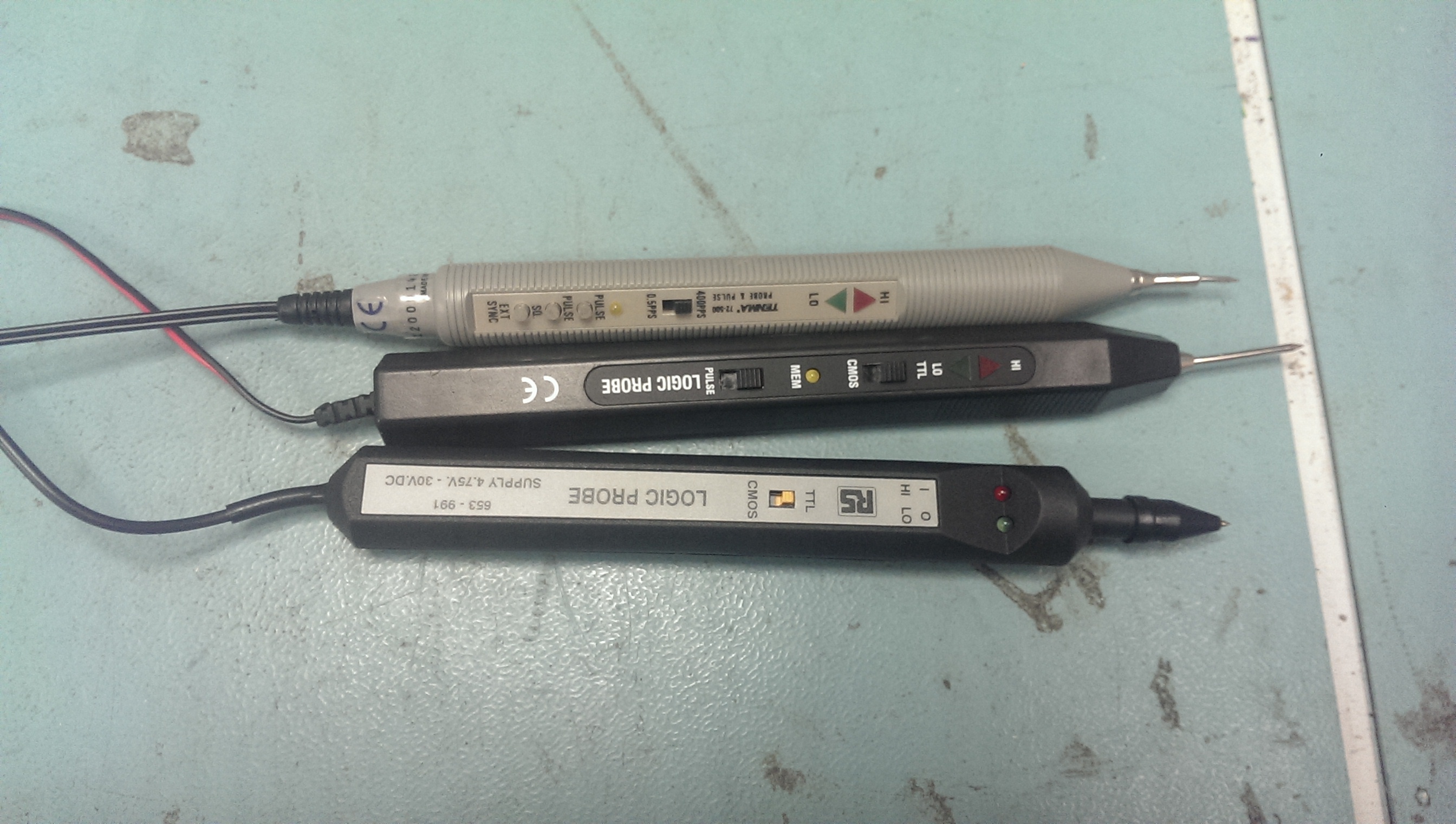
So here are what I’ve got.

Top one is a Tenma branded one (also seen this under different brand names). This is my probe of choice.
Second one is an unbranded one. Used this once and it feels really cheap in hand but it does have a buzzer in it to accompany the LED’s which is nice.
Lastly is an RS branded one. This is a recent eBay purchase bought mainly for this write-up.
First off, lead length.
There is nothing worse than being restricted but short leads when probing around a board.
Tenma = 58cm
Unbranded = 146cm
RS = 171cm
So my probe of choice has the shortest lead length. I must admit it has hindered me in the past.
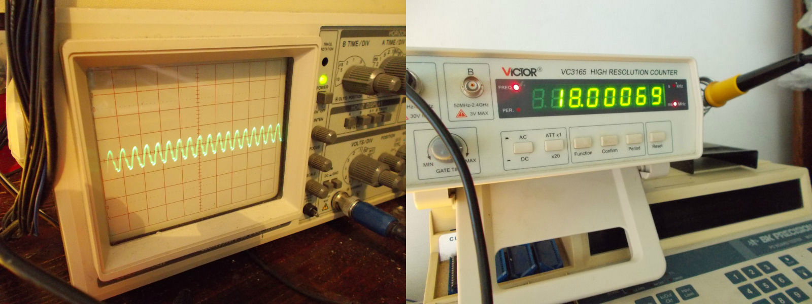
To test the logic thresholds I used my programmable PSU and used the outputs that have a common ground.
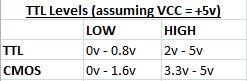
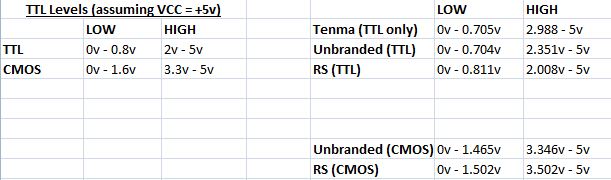
Here are the ‘official’ threshold levels according to Wikipedia for TTL and CMOS (assumming VCC = +5v).

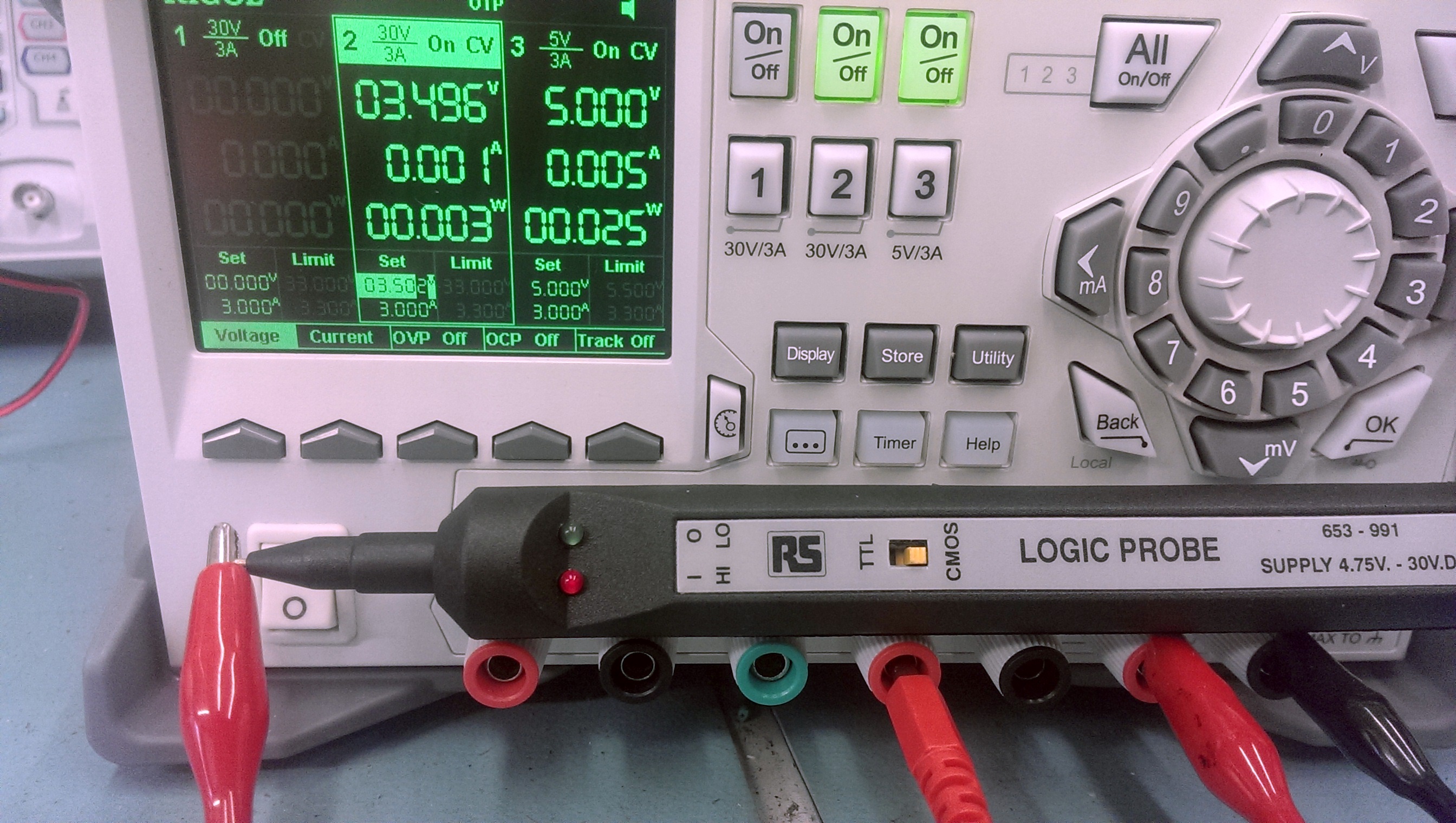
The pictures below show the voltage at which the LOW LED goes OFF and the voltage at which the HIGH LED comes on.
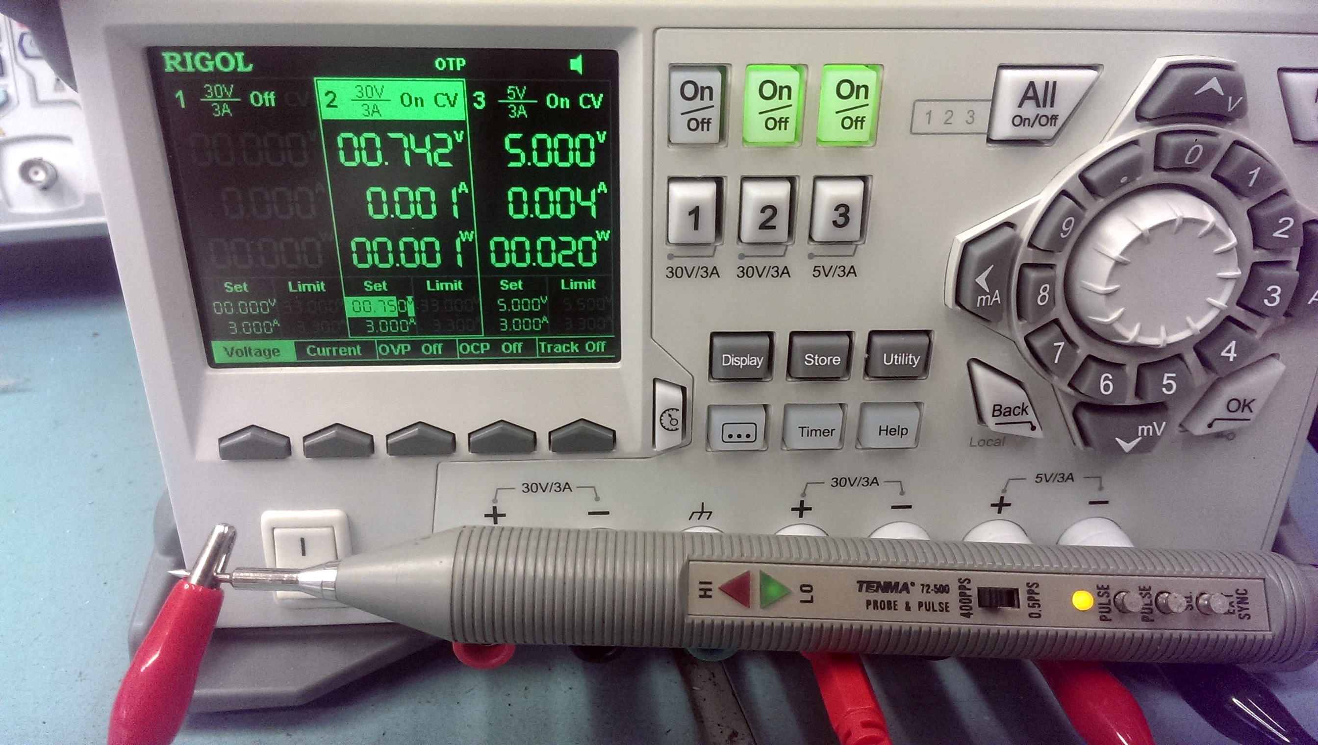
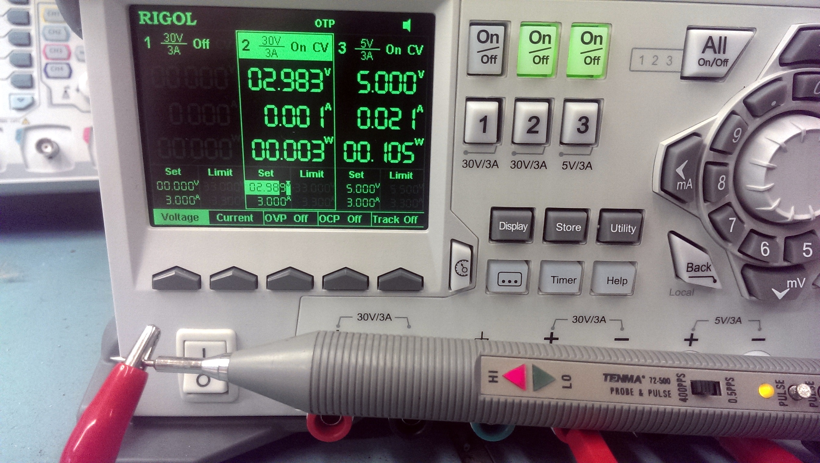
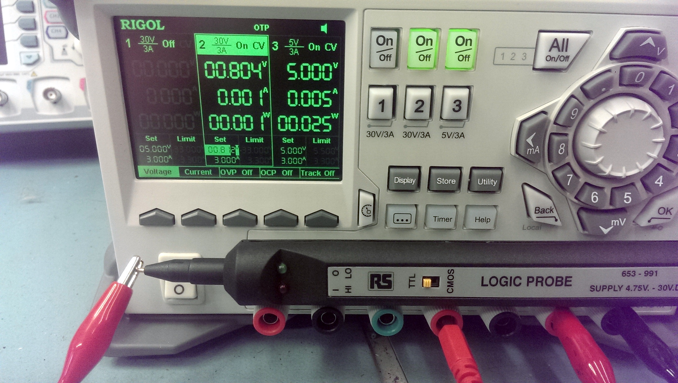
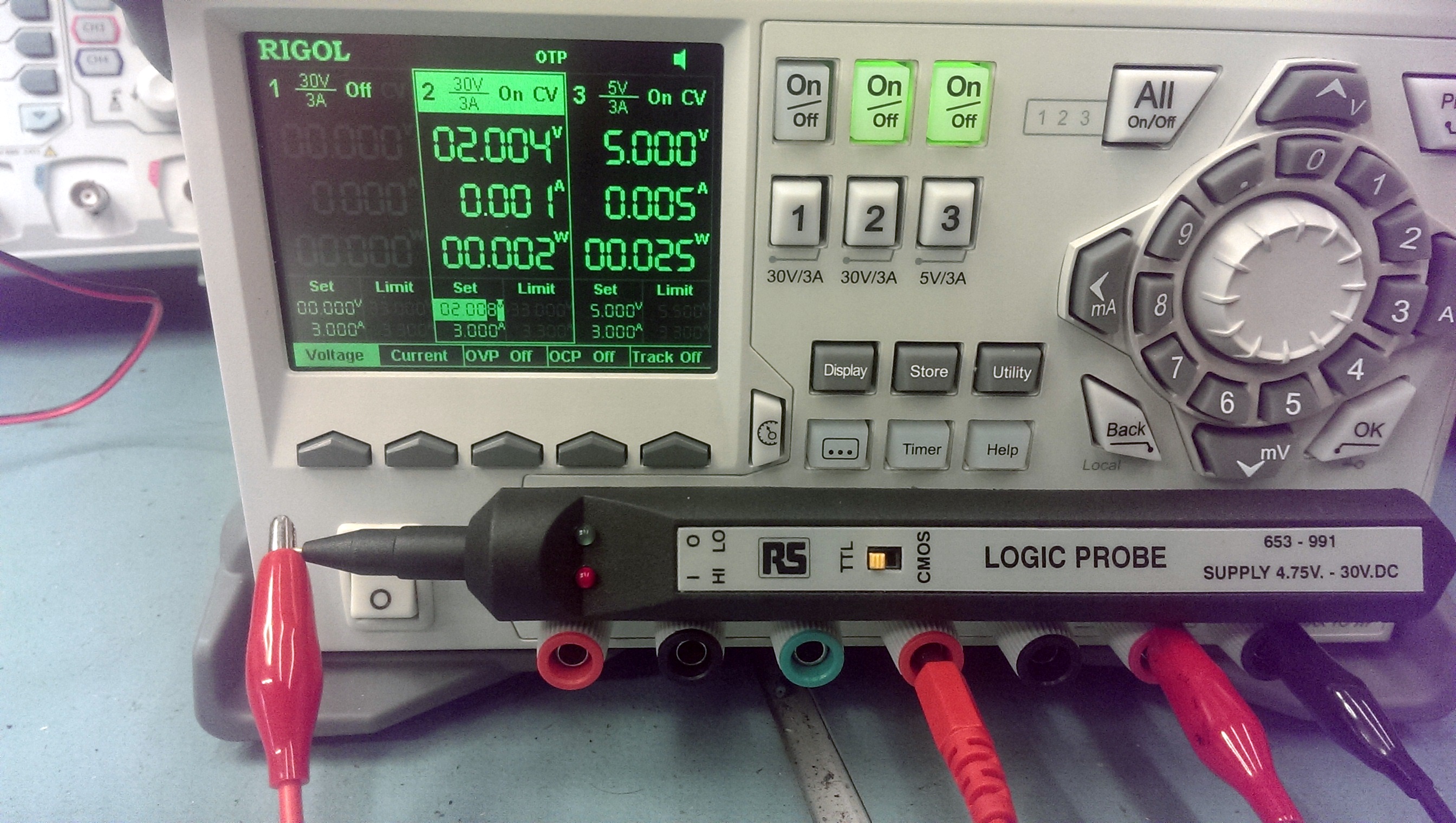
Lets look at the Tenma probe to start with.
This probe only supports TTL logic levels where as the other two can switch between TTL and CMOS.
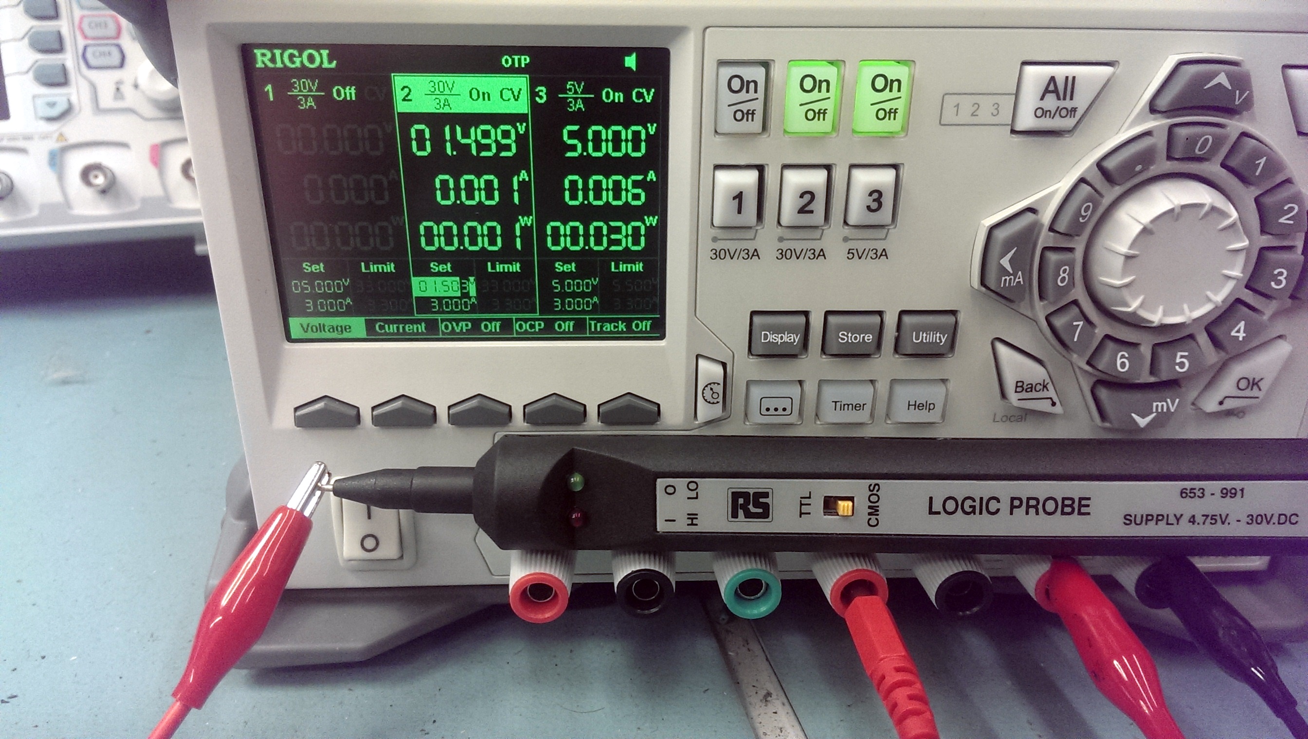
NOTE: You want to be looking at the smaller voltage settings at the bottom (under ‘Set’). This is the actual voltage settings and was checked for accuracy with a Fluke multimeter.
LOGIC LOW THRESHOLD (TTL)

LOGIC HIGH THRESHOLD (TTL)

As you can see the LOW level begins to show around 0.1v below the stated thresholds. Not too bothered about that. Whats more worrying is the HIGH trigger point, its nearly 1v out of spec.
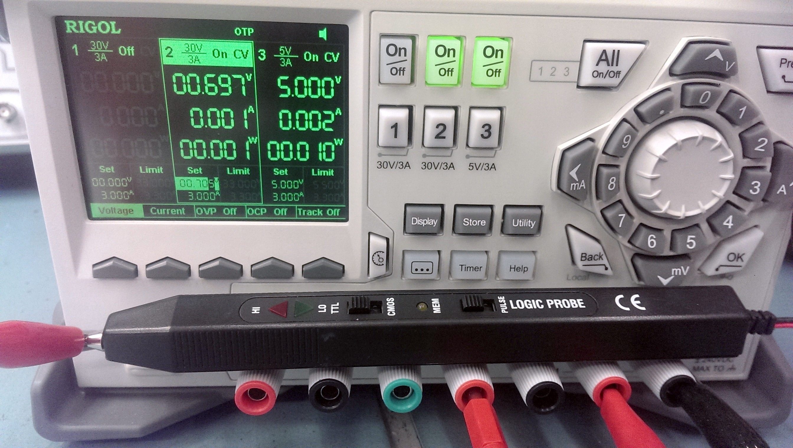
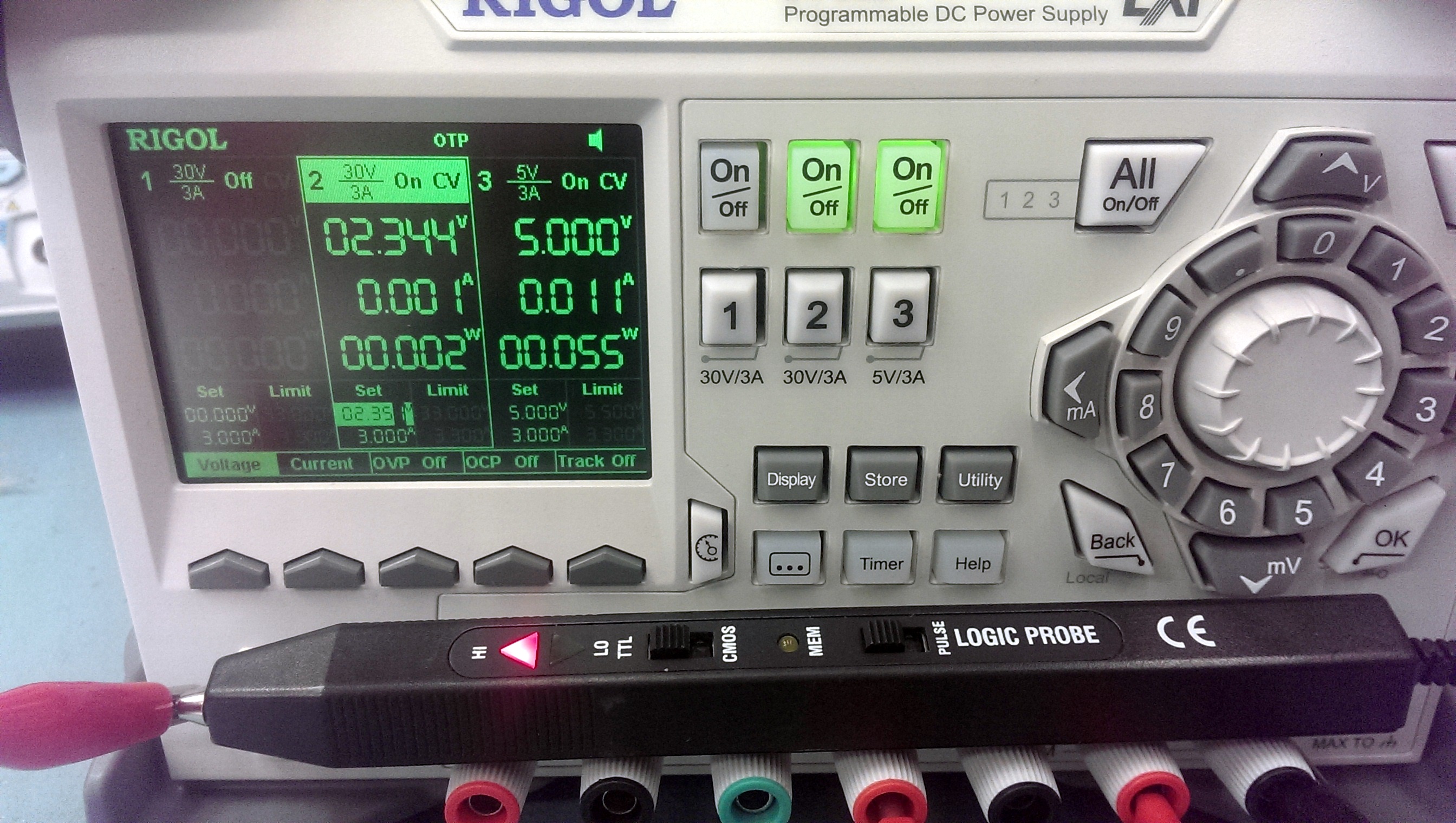
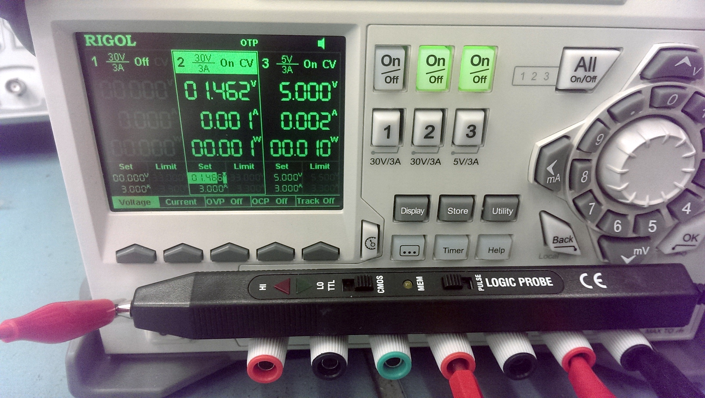
Next up is the unbranded probe
LOGIC LOW THRESHOLD (TTL)

LOGIC HIGH THRESHOLD (TTL)

This has similar LOW trigger levels as the Tenma one and the HIGH trigger is around 0.7v lower bringing it nearer to the thresholds stated. Not too bad.
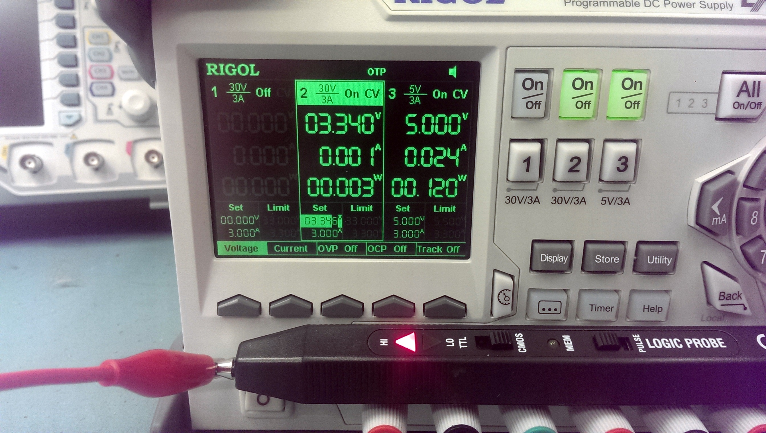
Finally the RS branded probe. The pictures are pretty useless here as the low brightness level of the probe at these voltages make it difficult to capture on camera but its there.
LOGIC LOW THRESHOLD (TTL)

LOGIC HIGH THRESHOLD (TTL)

Results are very positive for this probe on the TTL setting.
Next I test the CMOS setting. As the Tenma cannot support CMOS it is obviously excluded from this test.
Unbranded first.
LOGIC LOW THRESHOLD (CMOS)

LOGIC HIGH THRESHOLD (CMOS)

The LOW trigger is a bit low here but the HIGH is pretty good.
Now for the RS probe. Once again the pictures are pretty rubbish as the low level of the LED doesnt really show up on the camera but I assure you it is there.
LOGIC LOW THRESHOLD (CMOS)

LOGIC HIGH THRESHOLD (CMOS)

The LOW trigger is much the same but the HIGH is a little higher than the unbranded.
So here we have the full results

This test wasn’t the greatest and it is only my interpretation of it. For example, should I have taken readings when the LED’s were at full illumination? Different people will prefer different things.
The unbranded probe didn’t seem to have that dimming of the LED’s depending on the voltage. It was clearly either ON or OFF. Whether this is a good or bad thing will depend on user preference. For me its not too good. This probe however is the only one to have the buzzer which is a nice thing to have sometimes.
I think for me the RS probe will now be my probe of choice. It has nice long leads, feels good to hold and use and the results were decent too.
Got this NebulasRay PCB ( converted from another Namco NB-1 game) from my friend Josef for a repair:
For the uninitiated the game is a vertical shoot ’em up released by Namco in the 1994.It runs on Namco NB-1 platform.Here are the specs:
Board actually booted but didn’t pass the disclaimer screen:
As said, main CPU is a 68EC020.Probing it, revelead a good activity until it got stuck on the above screen, at this point most of control lines were going to high impedance state terminating the BUS activity.So, there had to be some trouble in the main code execution but, given the hardware complexity and lack of documentation, I was pretty lost.
I started to do some tracing on PCB so I could locate the WORK RAMs ( two Toshiba TC551001 @5C and 6C):
I figured out that they were not addressed directly by main CPU but through the near custom C351 (which is actually the custom sound CPU).I replaced both RAM but without luck.So, I removed the custom C351 and checking traces underneath it I found two breaks which I patched with some tiny wires:
With this fix the board passed the initial disclaimer screen but went straight into test mode although dipswitches were set to off.I quickly traced this to a missing 74HC253 multiplexer @4F:
Finally the board entered in game but all sprites were wrong :
Object RAMs are two Mitsubishi M5M5256 @20M and 21M:
A closer inspection revealed some loose pins that I promptly resoldered.In this way all sprites were restored except for jailbairs on some of them (like game title ):
All sprites ROMs are on the small daughterboard in form of 8 MX29F1610 FLASH devices :
Since the board was a converted one, they were hand soldered not in professional way (let’s say so..) so I reflowed them.Graphics and sound were perfect now but some inputs were missing or stuck like reported in switch test:
The inputs circuitry is so designed on this kind of hardware : JAMMA connector pin is connected to some EMI filter arrays , then to some custom CUS93 resistor arrays, then to some 74HC253 which combine inputs into outputs that go to the ASIC C160 (which is the I/O chip):
After some tracing I could pinpoint the faults in two bad CUS93 resistor arrays @2L and 1F:
Besides, there was intermittent contact between some pins of JAMMA connector and EMI network filter array @1K:
Board 100% fixed.End of (long..) job.
Today we have some new PLD dumps.
‘coolmod’ dumps the original PAL ‘VA63B’ @1 on his Varth (US revision B) CPS1 PCB.This dump replaces the handcrafted one made by Shoestring some time ago.
Andreas sent dumps from a Blood Brothers original PCB from TAD Corp.
They are made from 5 unprotected PLDs (GAL16V8 and PAL16L8) except protected U0242, U034 and U076.Dumps are untested because of a missing custom chip.
Thanks to both.
I dumped the three PLDs from a Macross Plus PCB.Original devices were three GAL16V8B, they were unsecured so I could read them with my EPROM programmer.
I got an Edward Randy with a black screen (but partial sound).
After a few checks with my scope, I quickly found a PAL @ location N5 with no signals on all of its outputs (BUT signals on its inputs).
As PALs from this game are not available yet online, I looked for other games that possibly shared the same hardware/system in order to try using a similar PAL.
And yes, that system is listed as “Data East Caveman Ninja Hardware” in MAME and some of these games got their PALs dumped. It was the case of Caveman Ninja and Robocop 2 that shares an almost identical PCB layout than Edward Randy (there are only a few differences in the GFX ROMs part).
So I burned the PAL at location N5 from Robocop 2 and plugged it on my Ed Randy board and here is what I got:
Well, at that time I was thinking it was due to an incompatibility between Robocop 2 and Edward Randy PALs and I temporarily gave up, waiting to get a dump from a working Edward Randy to be sure…
Then Shoestring confirmed me Caveman Ninja and Robocop 2 PALs @ N5 were strictly identical. It leaded him to believe that perhaps they are all common to each other and maybe there is a different problem with my board, which pushed me to have a look back at my board for possible other faulty chips. And he did well…
I started looking for other issues on the PCB and noticed that bending the board made the garbled graphics changing, even making them better looking at some point.
So I suspected the two SMC Data East customs labeled “55” having bad solder joints and reflowed the solder on them.
It then went way better. I had clean backgrounds in game, full intro with clean texts and pictures, title and Data East logo appearing (didn’t have all of that before) but no sprites in game. I noticed a square on the bottom-right corner that seemed containing garbled parts of sprites.
I then managed to find where the sprites part was located on the board and found two 6116 RAMs @ locations N9 and M9 that had suspicious signals on their data lines (pulsing but weakly and at low voltage). Piggybacking a known good working compatible RAM made parts of garbled sprites randomly appearing on screen.
I then desoldered one of the two RAMs (at location N9). With no big surprise it was tested bad on my programmer. I soldered a socket and put a new RAM in place. There was still no sprites but the garbled square on the bottom-right corner was not there anymore. Data lines on the new RAM were looking pretty much better though with strong pulses at 5V. The RAM located at M9 still showed weak outputs so I replaced it with another good known RAM:
Then sprites magically appeared !
Only one thing was remaining: the voice generating chips (2x OKI M6295) were missing so I replaced them and got the sound fully working.
I played the game several times since that and it is working perfectly.