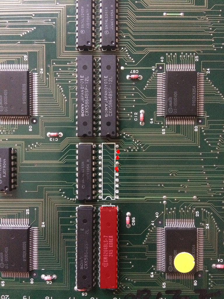
Shorting some data pins rams I found the one responsible for the tiles arrangement.
I replaced the one marked in red below and it was infact faulty but it didn’t fix completely the problem.
I noticed that the 74ls745 above it was pressed down badly like if it was hit but something.
I decided to unsolder it and test the continuity of all the pads and infact I found three of them (marked in red) that visually were OK but they had no continuity
with the other chips.
That meant that the internal pad was broken so bad it detached internally
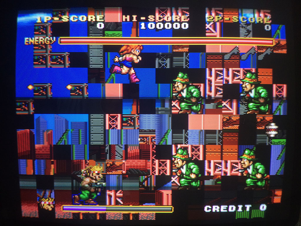
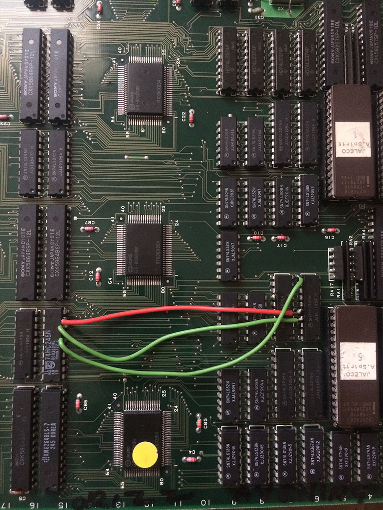
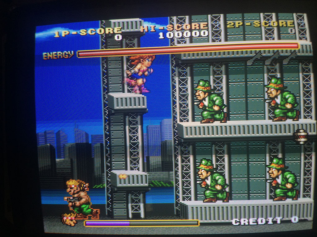
Making some ugly flying wiring with something I had at hand I tested the game which was fully restored
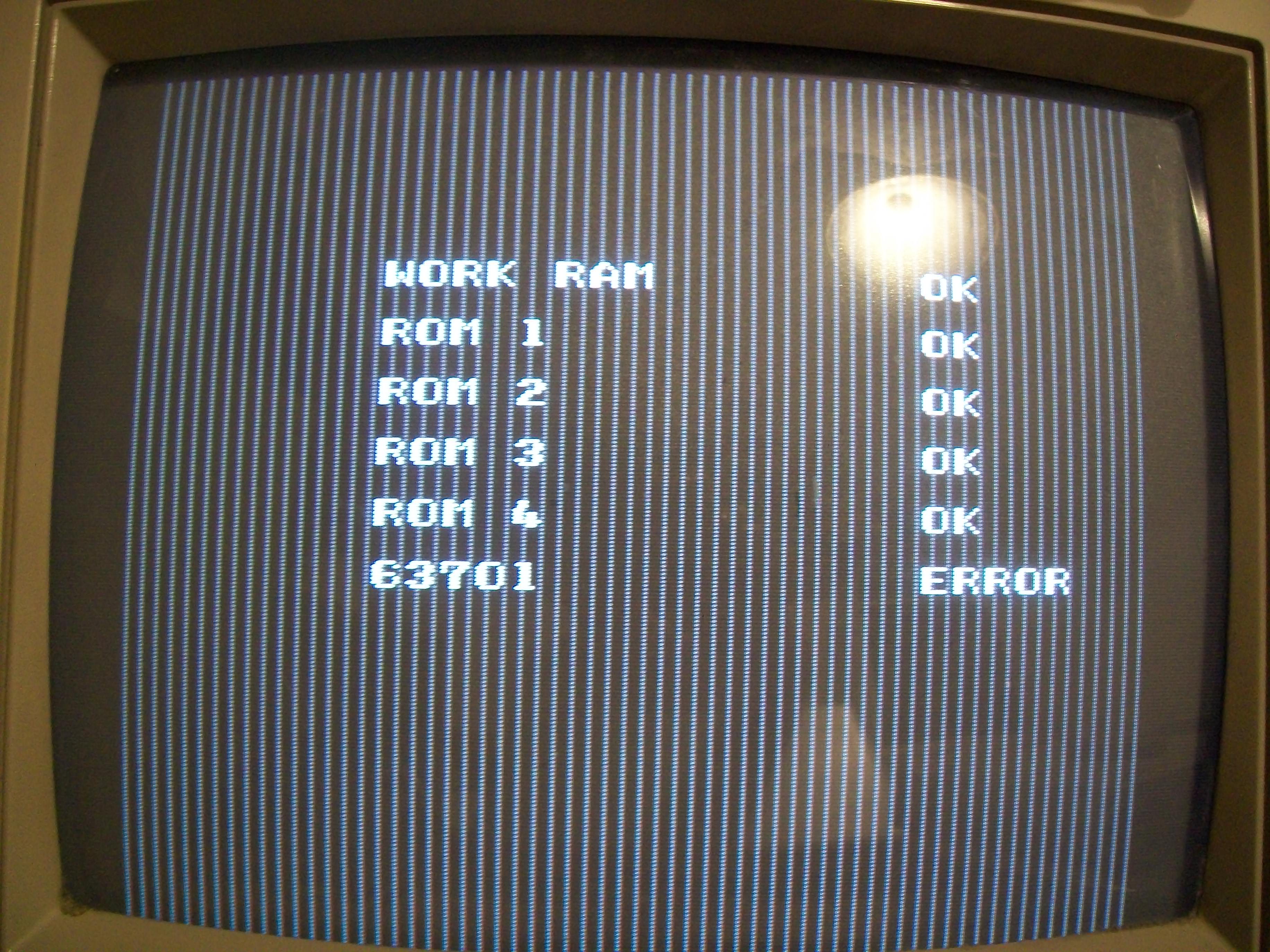
but it didn’t pass the self-test sitting on a ‘63701 ERROR:
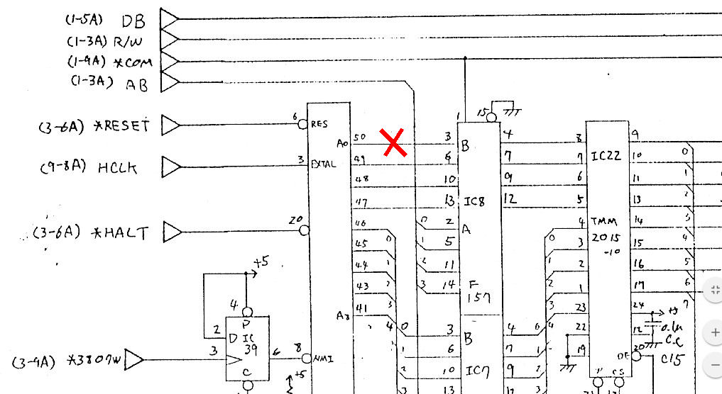
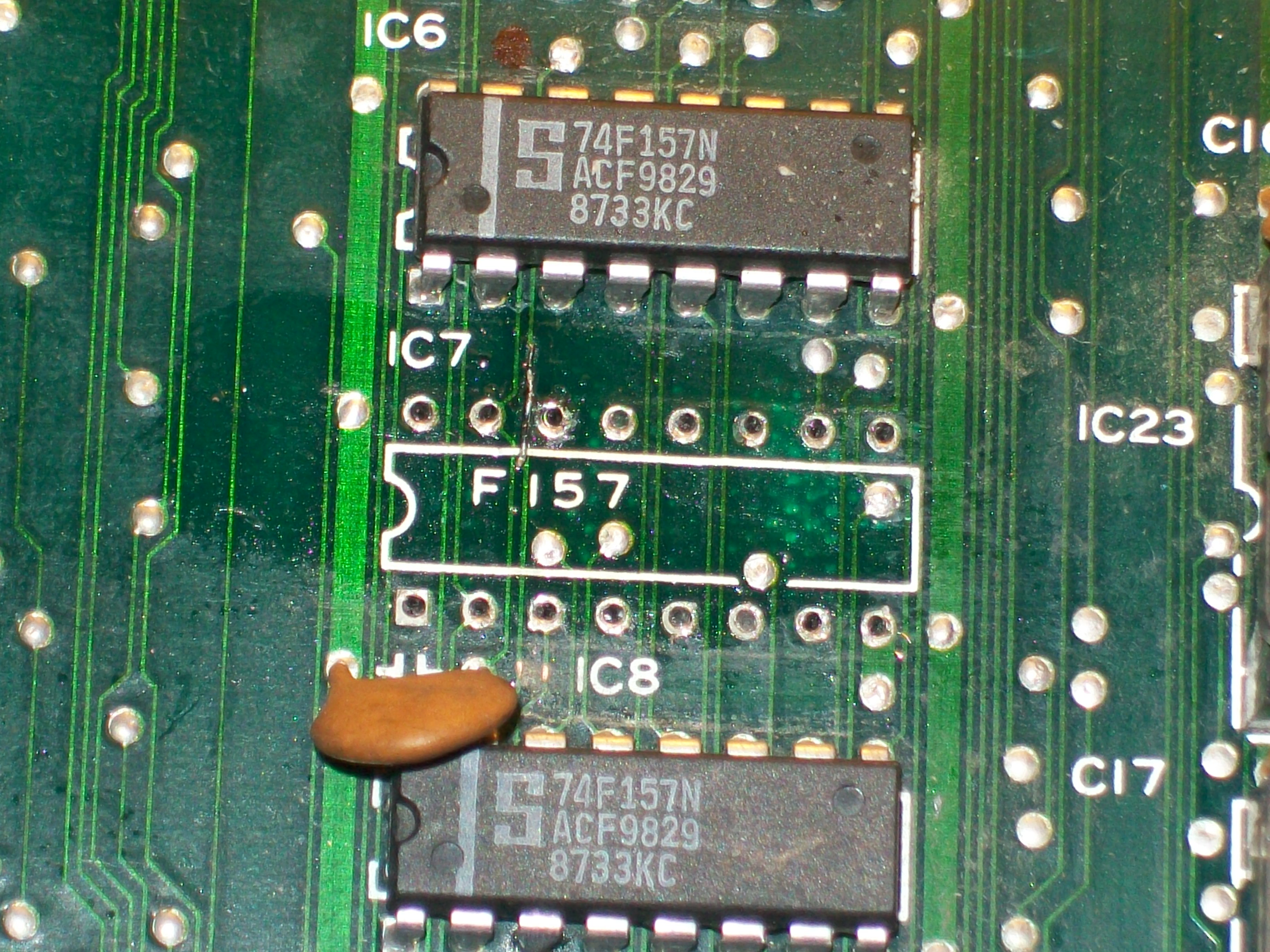
The /HALT line of the HD63701 MCU was asserted, this was sign of some trouble in its busses.I swapped a good chip with no change so I went to look at schematics.All was good until I found no continuity between the address line ‘A0’ (pin 50) of the MCU with pin 3 of the 74F157 @IC8:
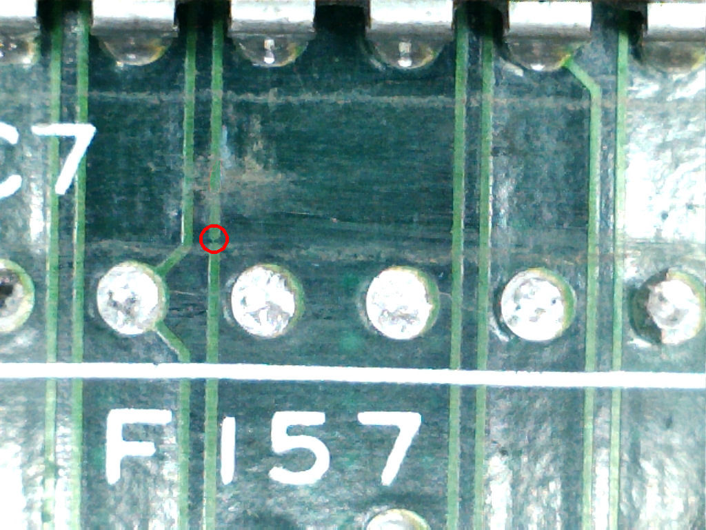
Tracing back the address line I could figure out where connection was interrupted, exactly under the 74F157 @IC7 so I removed it.Inspecting the involved area with a USB microscope revealed a corroded trace :
I patched it with some AWG30 wire:
With this fix finally the board passed the self-test but two issues were present in game : sound was missing and backgrounds had jailbars :
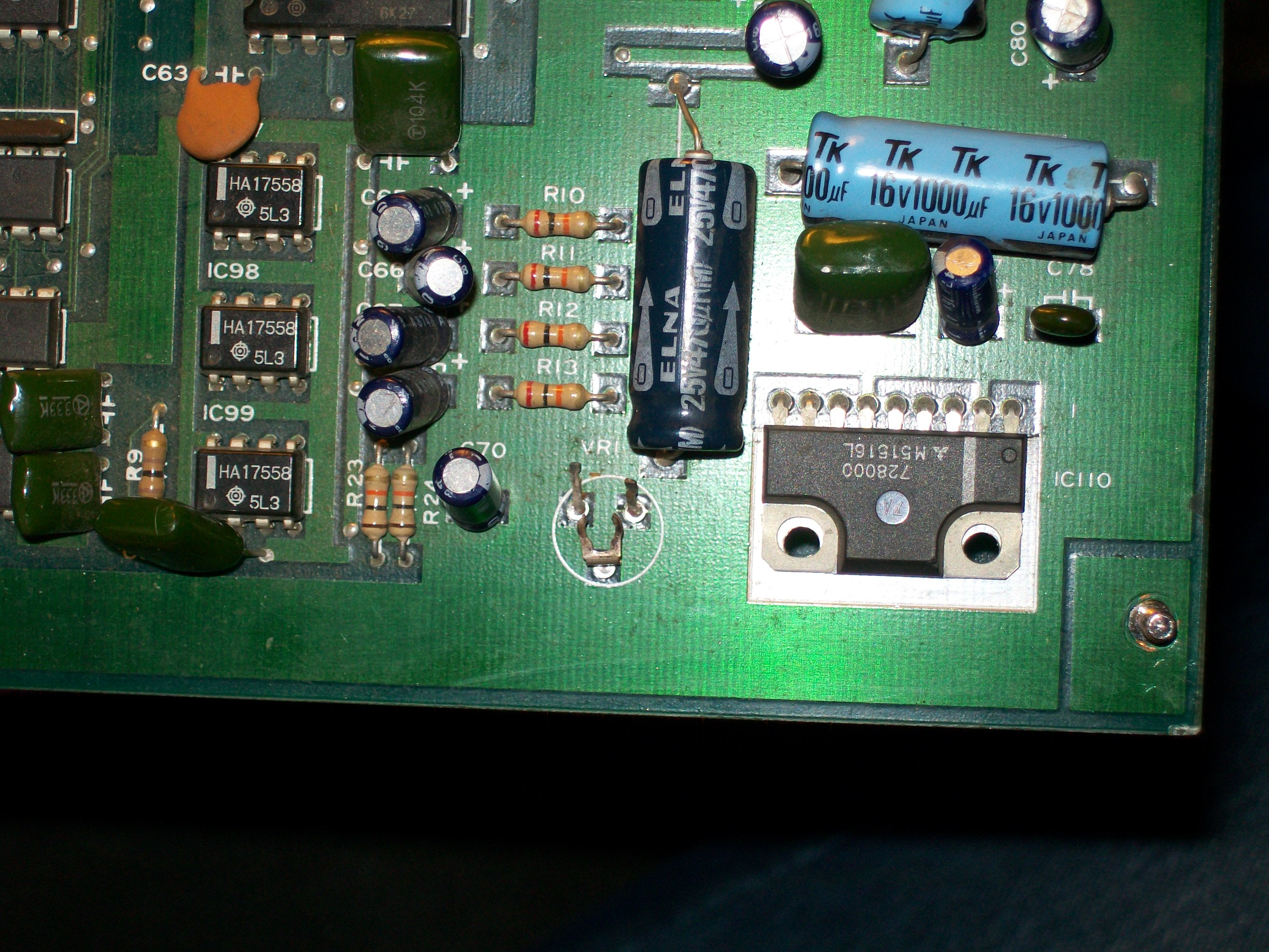
The first issue was due a missing 10Kohm potentiometer in the sound section:
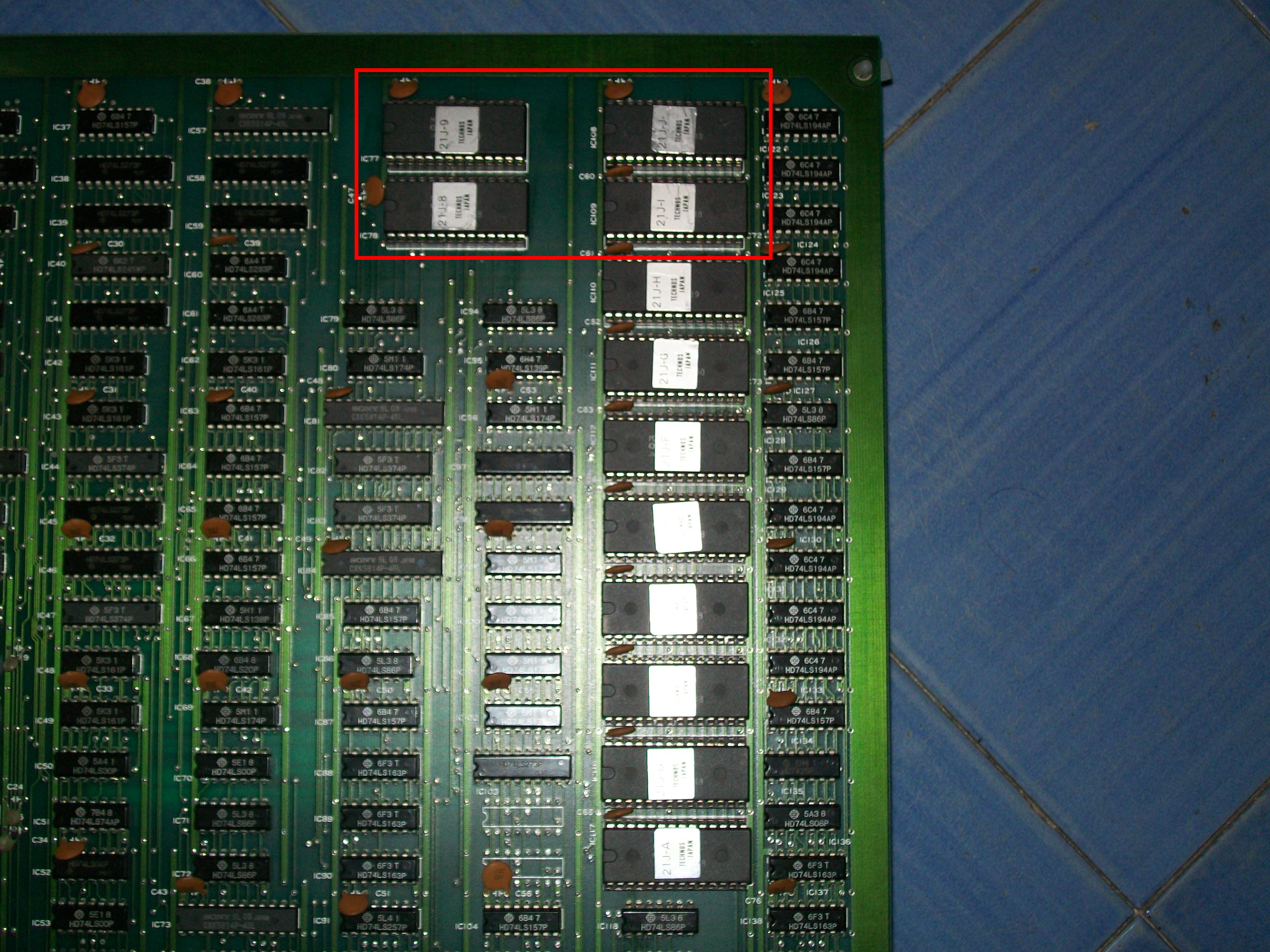
The backgrounds GFX data are stored into four 27512 OTP devices on video board :
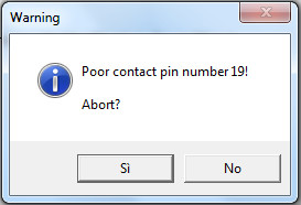
When I went to dump the ones @IC108 ans IC109 my programmer warned me about a bad contact on pin 19 (data line ‘D7’) of both :
Obviously the resulting dumps didn’t match the ones from MAME ROM sets so I programmed two 27C512 EPROMs as replacement.This restored graphics completely.Yes, yet another Double Dragon PCB fixed!
PCB Repair LogsComments Off on Alpha Denshi Co. (Equites and Splendor Blast) double repair log
Oct182016
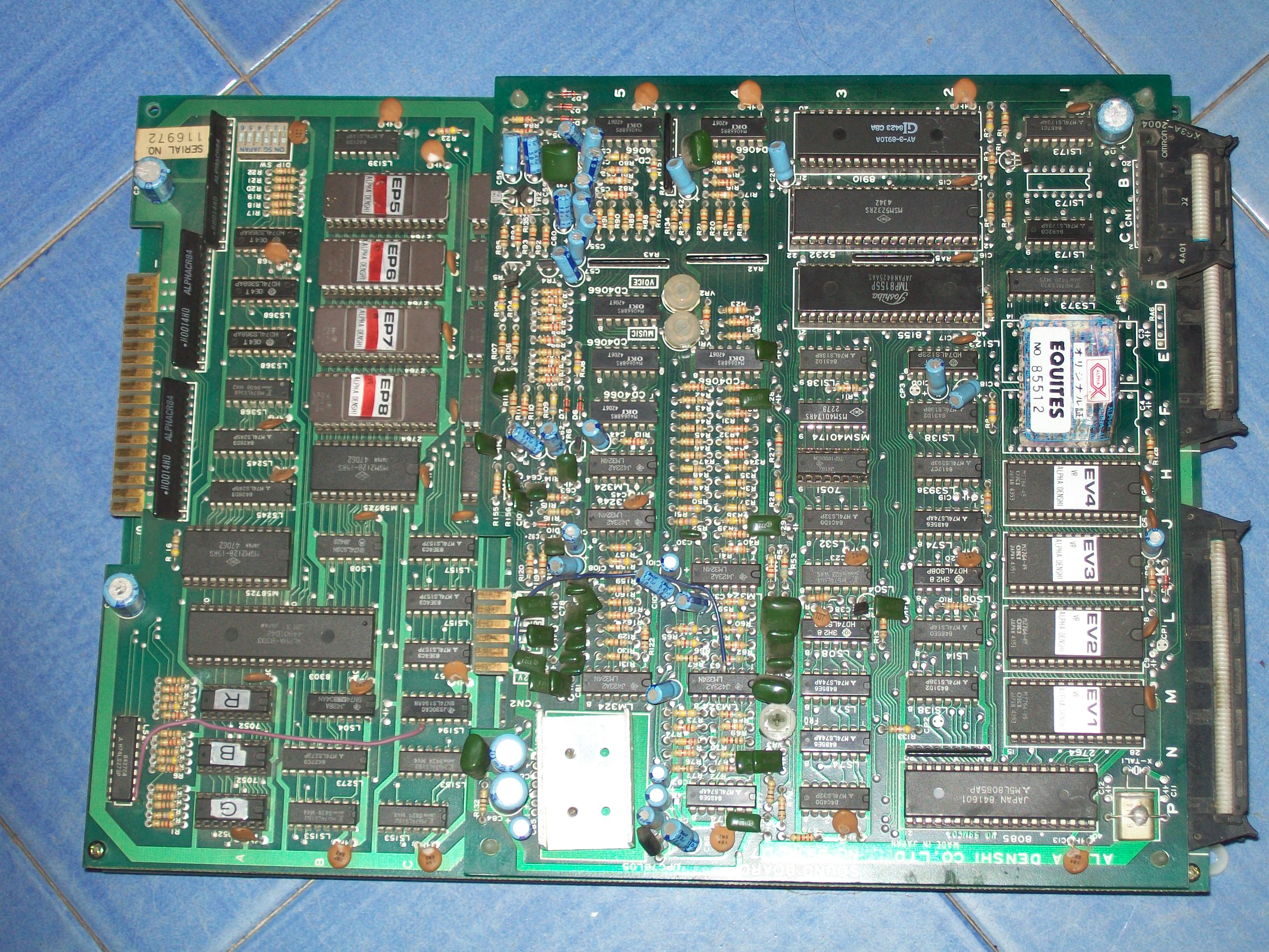
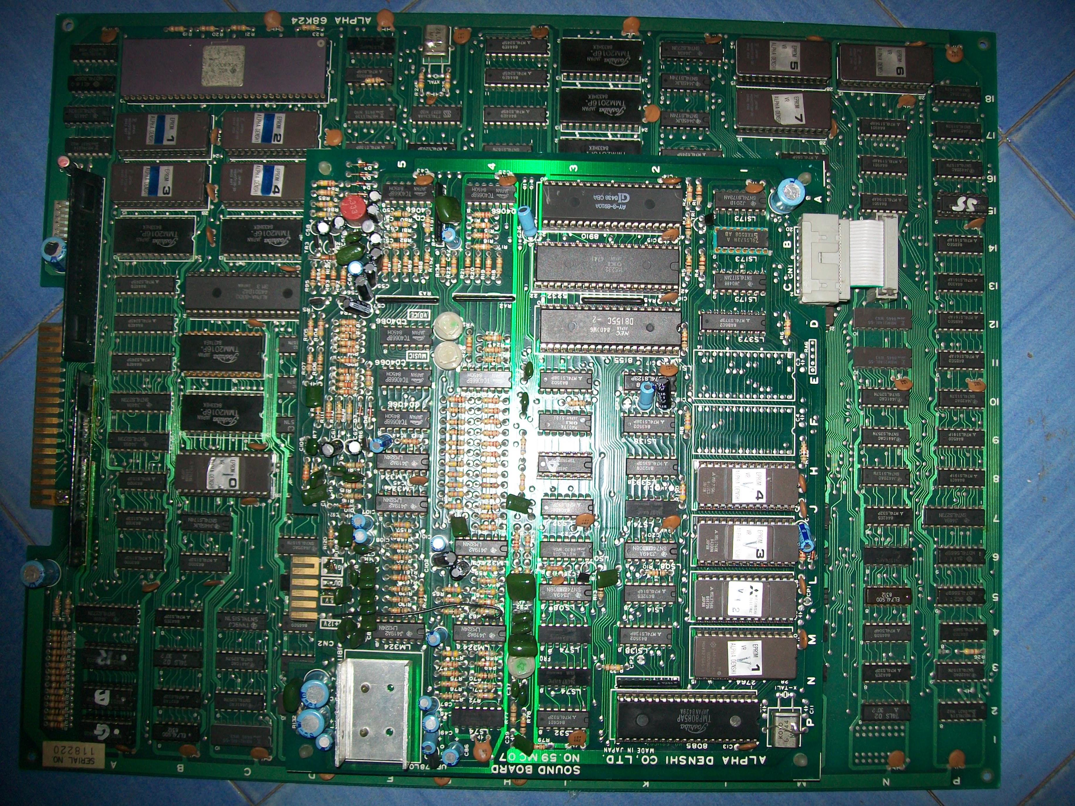
I got two rare boards manufactured by Alpha Denshi for repair : Equites and Splendor Blast
Here’s Equites :
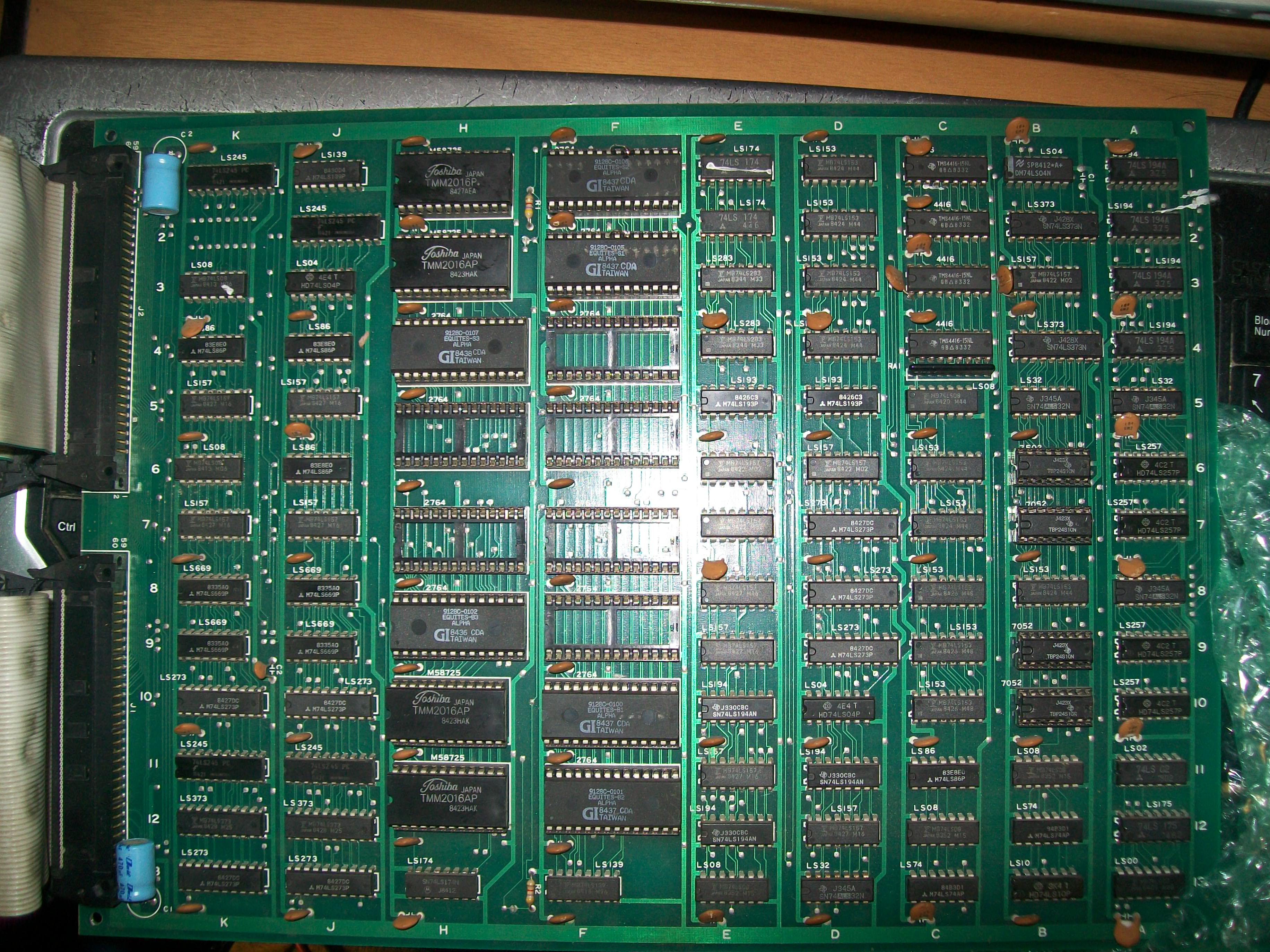
Board played fine except for jailbars on some sprites (look at explosions and first enemies on the ground in the below video):
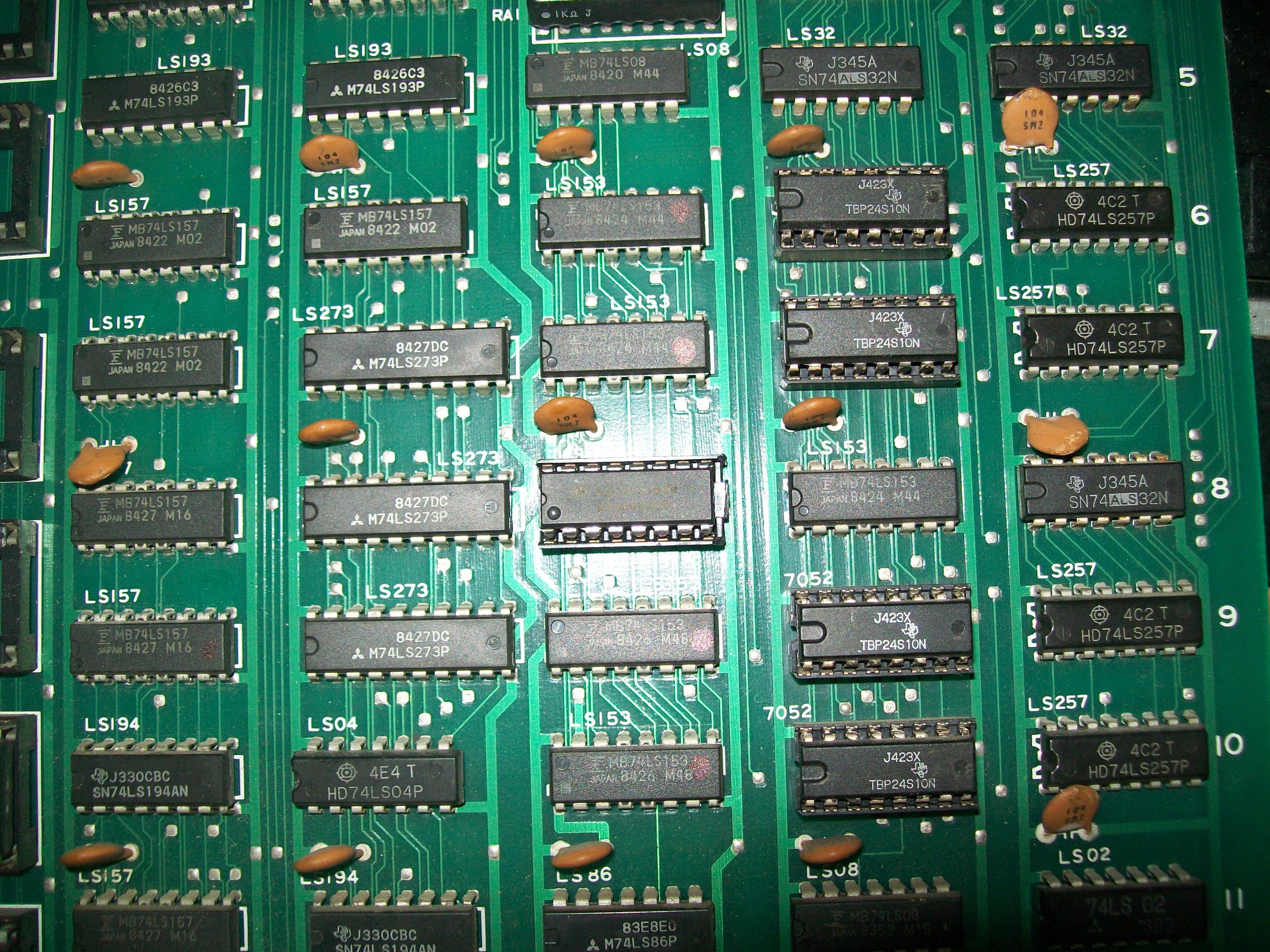
All the GFX generation circuitry lies on bottom board:
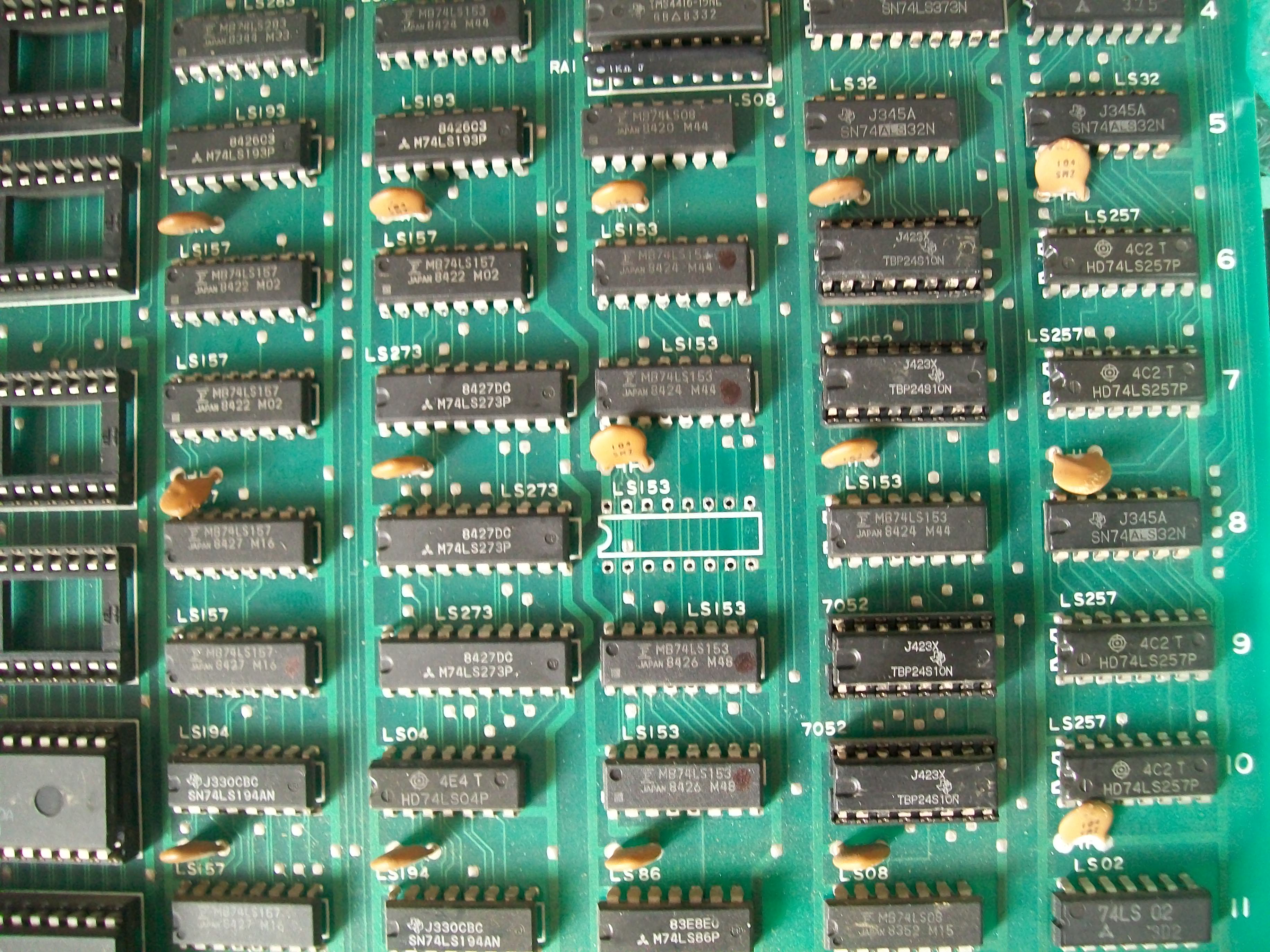
A lor of TTLs were from Fujitsu (especially multiplexers 74LS157 and 74LS153) so I went to check them with my logic comparator.All passed the test except for the 74LS153 @8C:
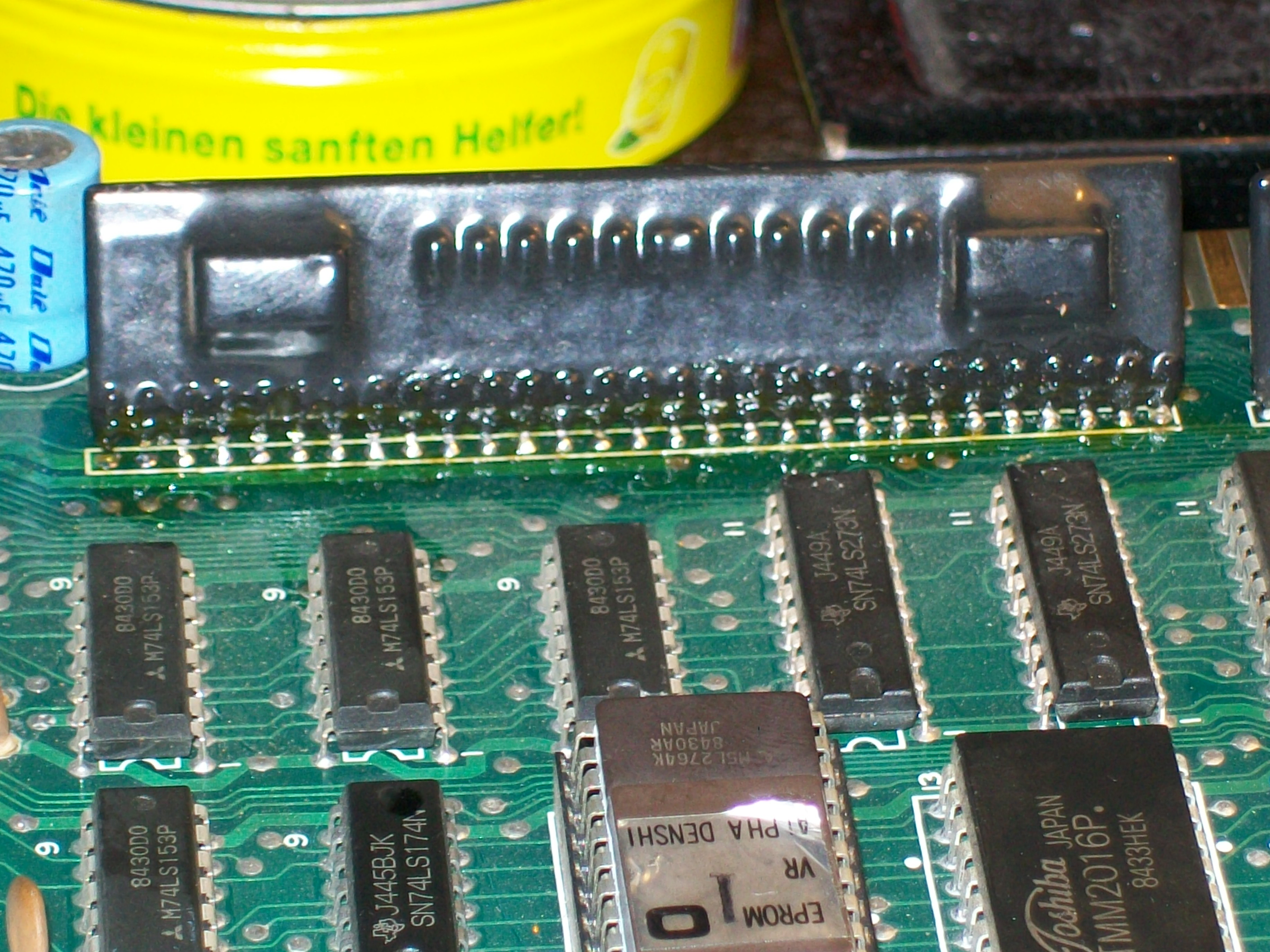
I desoldered it:
The chip failed when tested out-of-circuit:
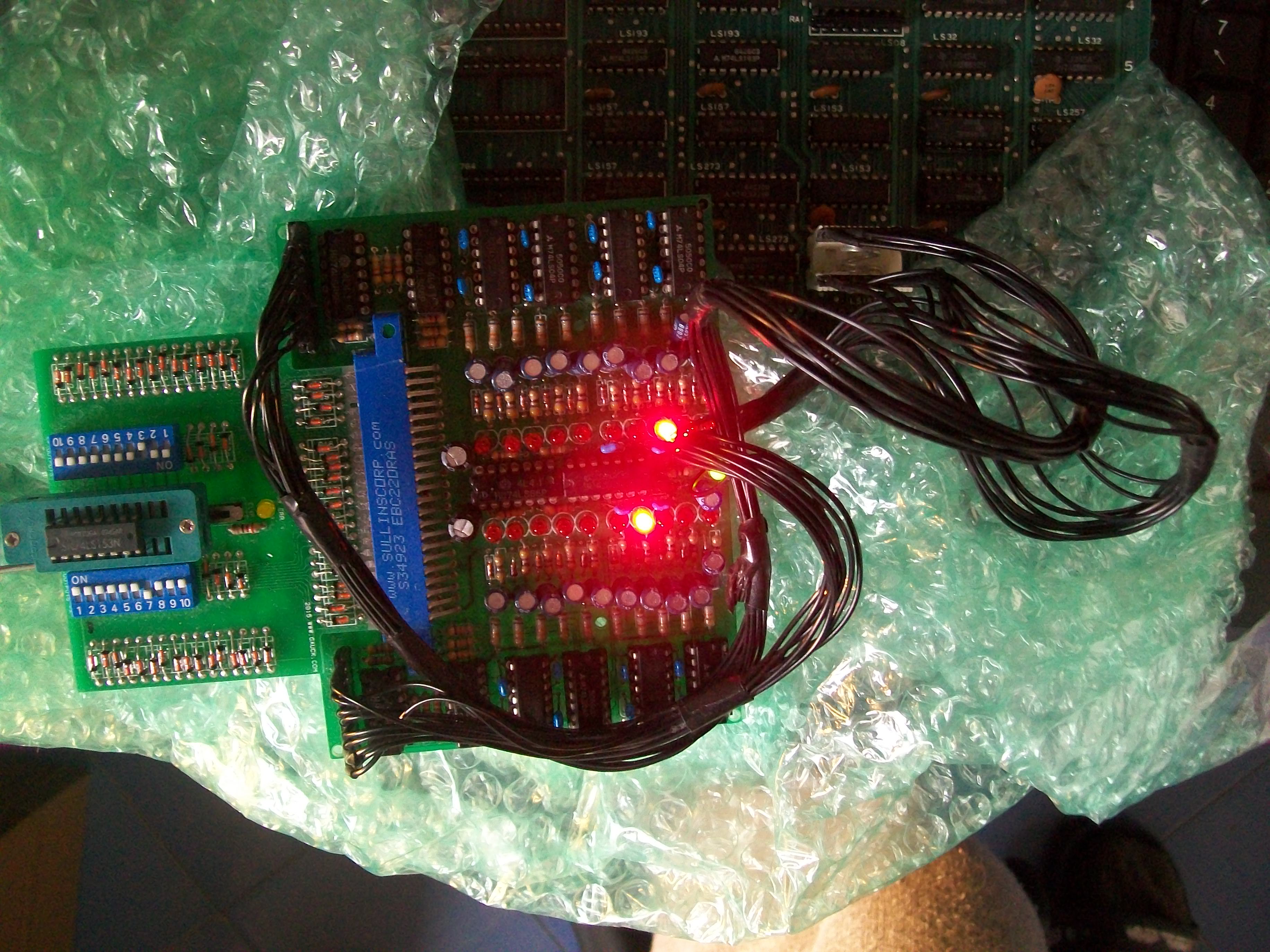
I added a socket and a good chip:
No more glitched sprites and board 100% fixed:
Here’s Splendor Blast:
This was a little tricky.When I first powered the board up, watchdog was active, the self-test was failing in all program ROMs and in the ‘ALPHA-8303’ MCU RAM:
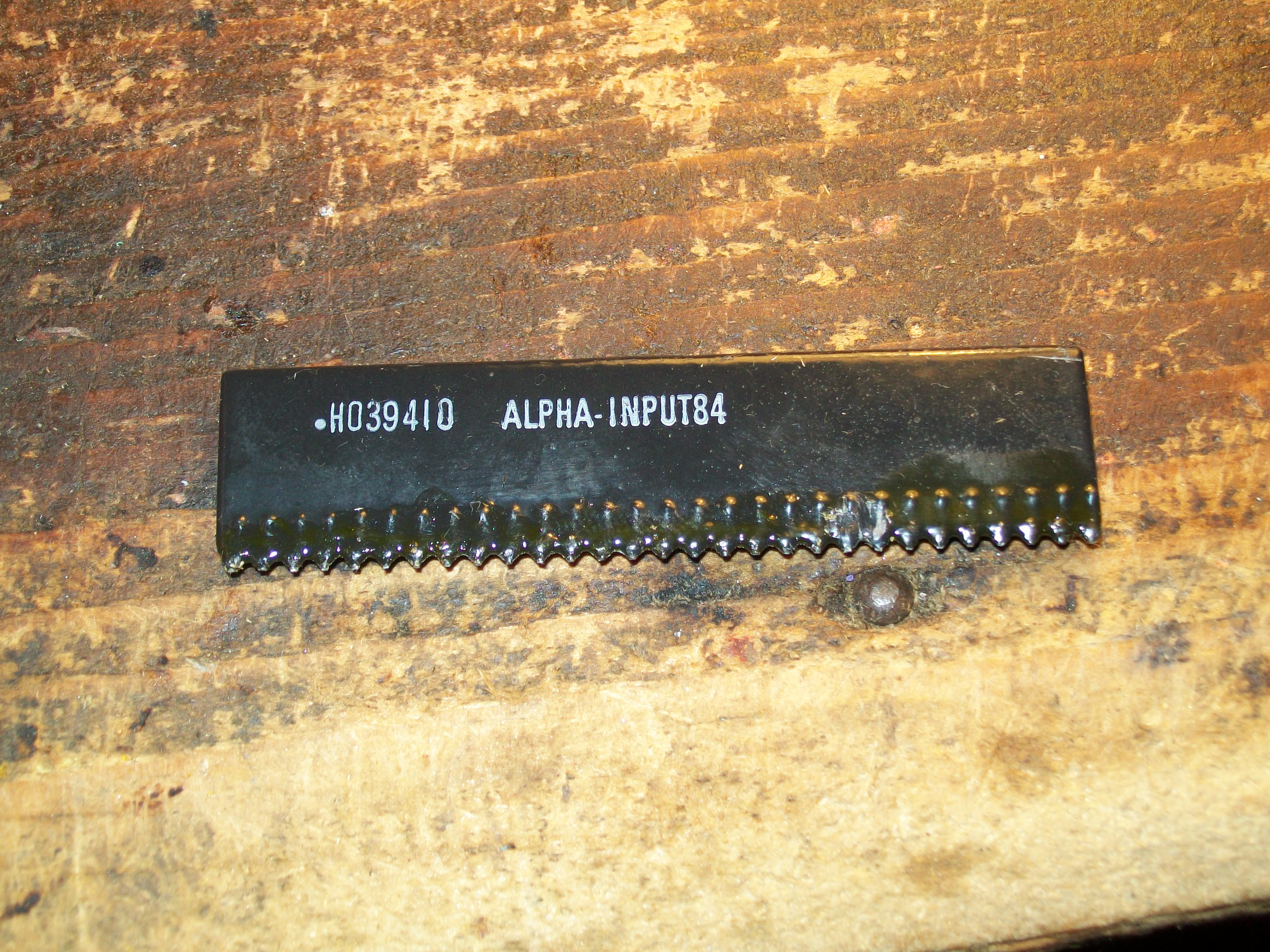
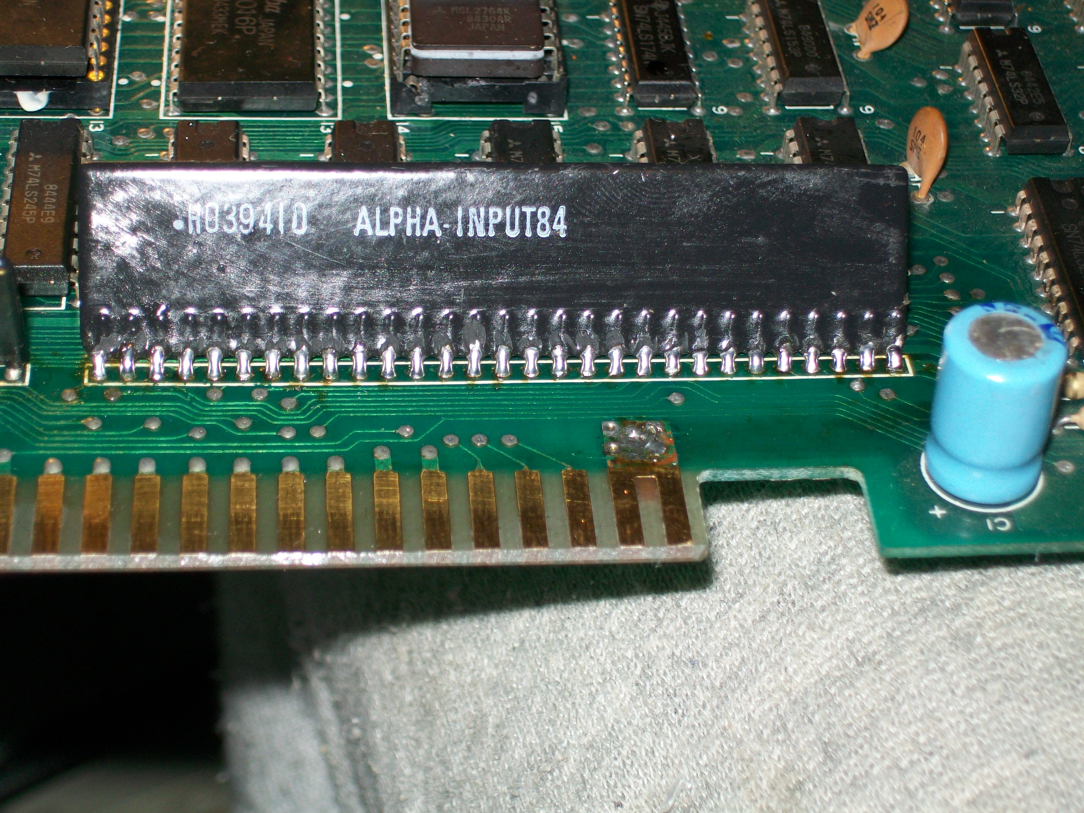
Doing a visual inspection of PCB I noticed that one of the two custom SIL marked ‘ALPHA-INPUT84’ was wonky :
It came off in my hands when I touched it:
I powered the board without this component and board successfully passed the self-test so I resoldered it (most likely it was corrupting the main 68000 CPU data bus since some lines are shared with it) :
As I said, the board entered in game but some sprites showed jailbars:
The three sprites ROMs are in bottom board:
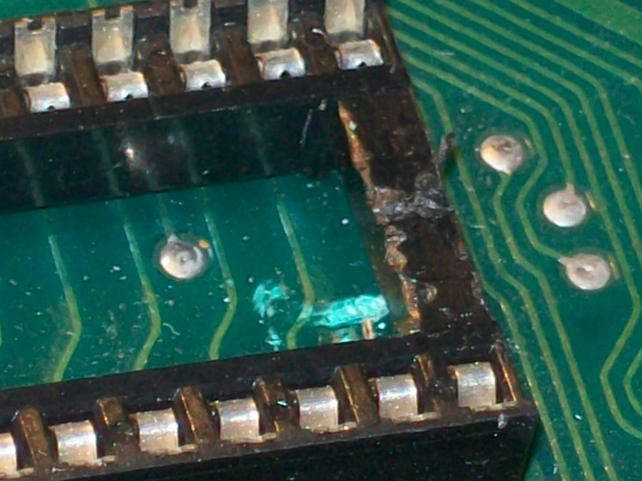
I dumped them and they were good.With my multimeter I figured out that address bus was shared among the three EPROMs while data bus was in common only among ROM 5 and 7.But I could not measure continuity between pin 15 (D3) of these two.I removed the devices from sockets and found a severed trace underneath:
This Thunder Cross II board was stuck in a watchdog cycle.
A quick visual inspection showed this
It was easy enough to bend this back a little without causing any damage.
Powering up the game, it would sometimes show the RAM/ROM test screen from the POST with failures reported and sometimes it would just reset straight away showing nothing.
Using a logic probe I quickly found the RAM at 1H and 16E were bad both of which had completely dead output pins.
I piggy backed a known good working 6116 RAM chip on top of both of these and while it didn’t cure all my problems, on the time it booted to the test screen these RAM’s now showed clear.
I replaced them and moved onto the resetting issue.
The reset on this board is handled by a custom SIP package. I was fairly sure this wasn’t to blame as on the occasions it booted up, if I held the TEST button down to reinitialise the EEPROM the game did not reset throughout the initialisation.
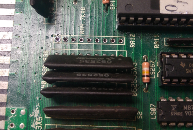
I did notice a 4.7k resistor array was missing.
I replaced this but it made no difference.
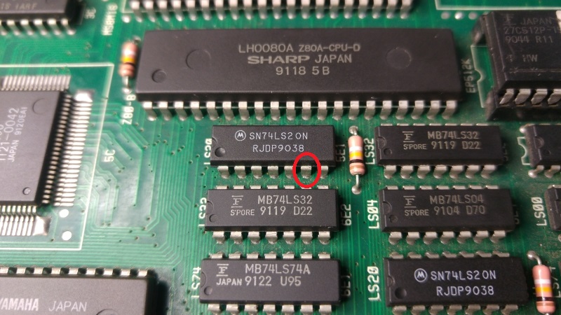
Next I noticed the game booted up more regular if my hand was on the 68000 CPU. Things like this are a good indication that there is a floating pin somewhere. Probing the CPU pins revealed that pin 21 of the 68000 (/VPA).
Chasing this proved difficult as there was a broken trace somewhere but these Konami boards have really small thin traces and vias. I eventually traced it back to pin 6 of a 74LS20 at 5E1.
Jumpering this gave me a booting game.
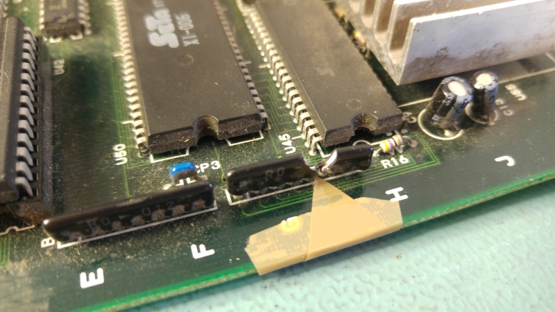
Everything initially looked good, the attract mode played and the sound effects were present. The problem came when some music played. To start with it sounded terrible but once the music stopped all the sound effects were either messed up too or were missing altogether.
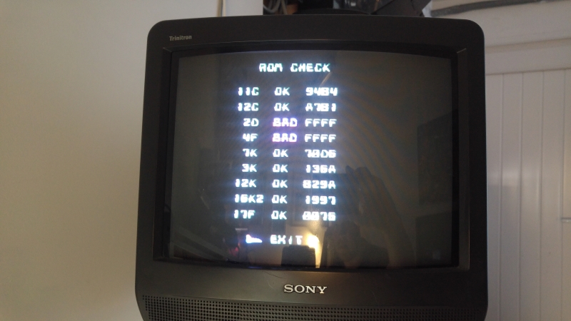
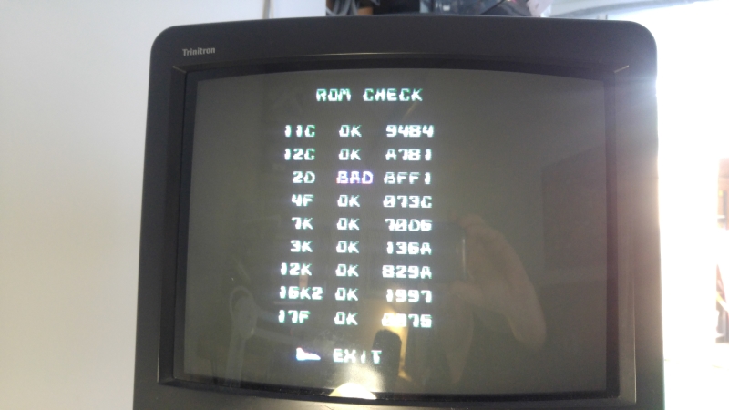
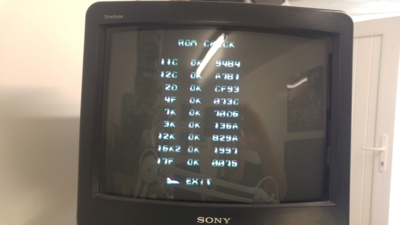
I fired up the test mode and did a ROM check which game me this
or sometimes this
I had verified the ROM which checked out OK and sound effects were present. The music also attempted to play so I was fairly sure the CPU and ROM were good.
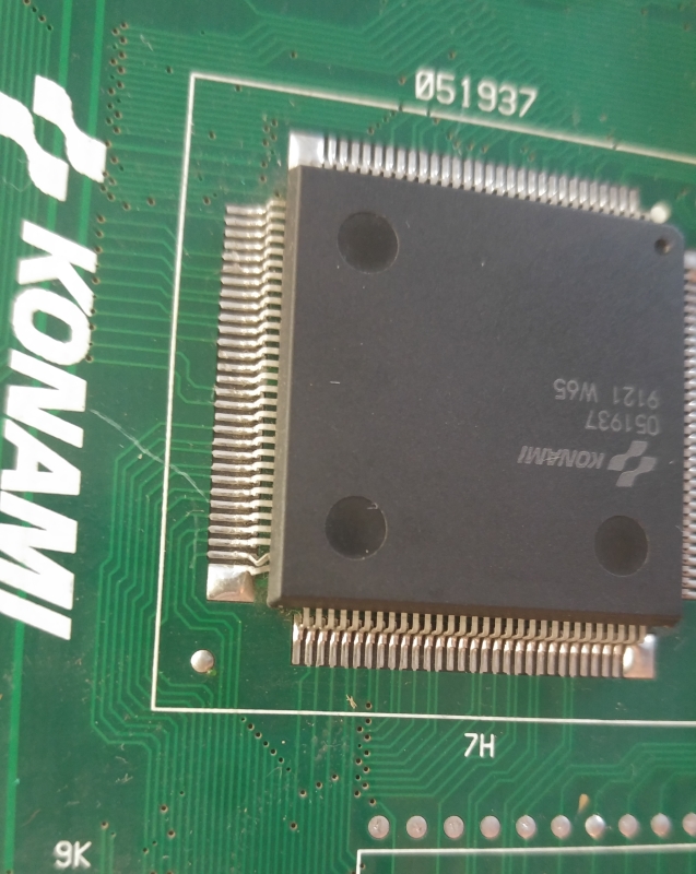
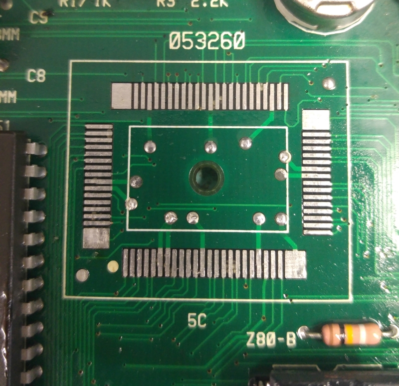
I started looking at how the MASKROM was addressed and how the PASS/FAIL data was send back to the main CPU. This all led me to the 053260 custom chip at location 5E
I mapped out all the address and data line to the MASKROM and noticed that anything after address line A10 was dead. Looks like we have a dead custom.
As it happens I found a scrap Konami PCB in the loft from which I could harvest this chip from.
Replacing this gave me my sound back and the ROM tests now all pass.
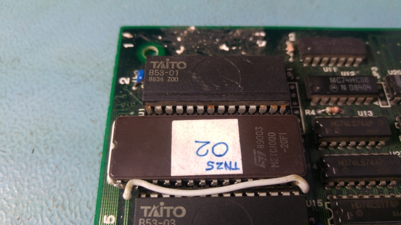
Got a bunch of boards from Olly to attempt to repair. One of them is a tiny New Zealand Story PCB.
There is a broken custom resistor array on this PCB. Turns out this SIP is for DAC for the green colours.
Not really sure how this could have happened. Caius is sending me a replacement for it but it plays no further part of this repair.
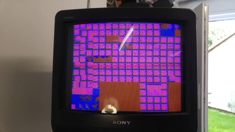
I powered up the PCB and this is what we get
The game plays blind behind this wall of garbage so we know the CPU is doing its job.
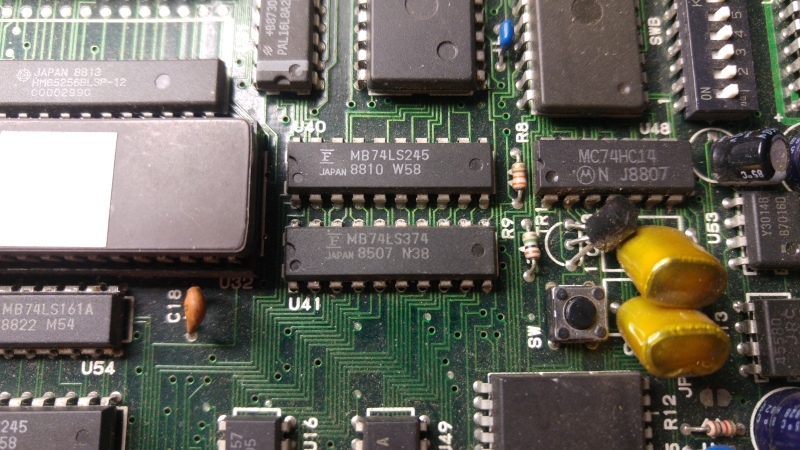
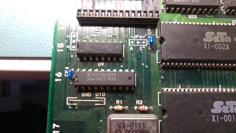
The board has quite a few Fujitsu TTL chips on it so my first bets were on failed TTL. The PCB is also tiny which makes this job pretty quick.
In my experience of failed Fujitsu chips I found that pins go completely dead and this PCB was on different. I found a couple of 74LS374 chips at U41 and U10 with dead outputs and these are easy to spot with a logic probe.
As the outputs were dead I could quickly test by ‘piggybacking’ a known good chip on top of it. The changes were good enough to confirm.
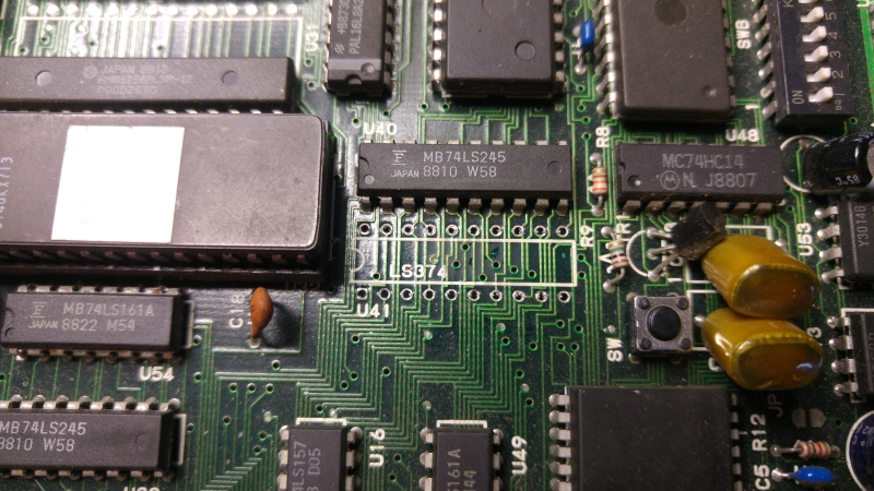
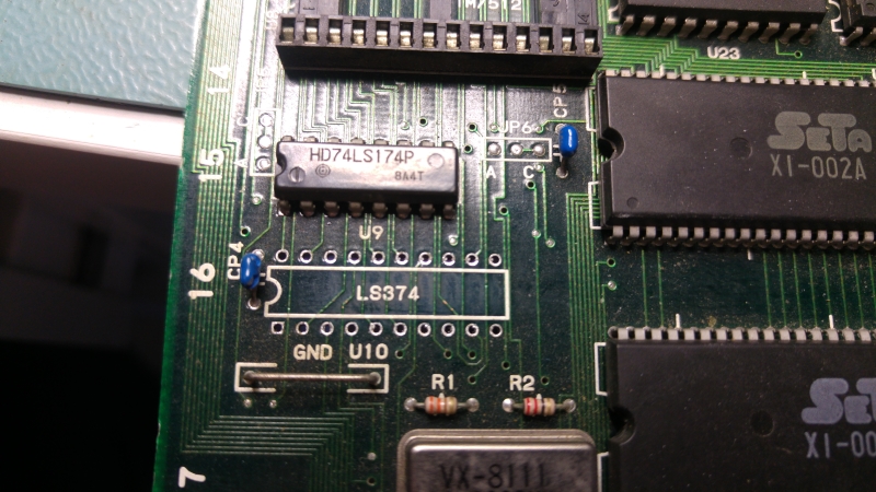
I replaced these two chips.
Replacing them did give a big difference and I could now see all the outputs from those two chips were once again active. The graphics were all messed up still.
Next I see that one of the MASKROM’s has been replaced. They are 23C1000 compatible and therefore there is no 28 pin EPROM replacement available. It has been replaced with modified a 27C1000 chip.
This mod is not part of the problem.
I pulled all the other MASKROM’s and dumped them. 4 of them actually failed so in the short term I replaced them with modified 27C301 EPROM’s.
All the graphics came back good.
There is a 128×8 ROM replacement PCB available from OSHpark shared projects made by system11 so I downloaded the Eagle board file, added a little TNZS graphic to it and ordered some up. The A298010AV chips however are really quite hard to source so Ive got to wait until February before these come in from back order!
As it stands now the game is fully playable with only the green colour issue. I will replace the resistor array SIP once it gets here.