PCB Repair LogsComments Off on Teenage Mutant Ninja Turtles repair log
Apr222019
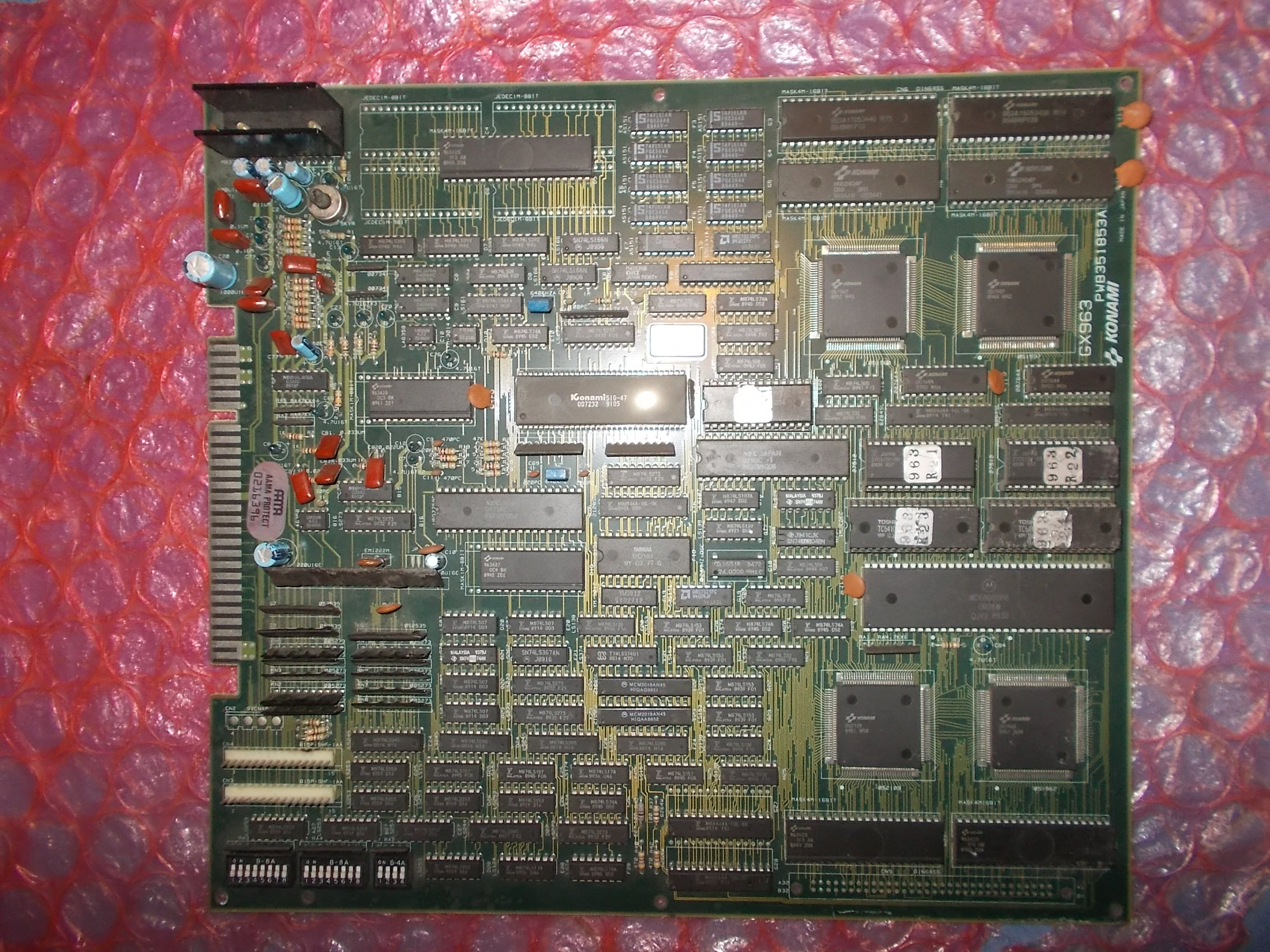
Got for repair from the States this Teenage Mutant Ninja Turtles PCB (actually the US 4 Player ROM set)
Board booted up with noticeable graphical issues, both sprites and backgrounds were affected as they were missing parts.Also colors were wrong, screen was blue tinted (hard to distinguish in the video and pictures though)
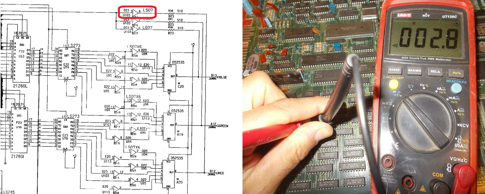
The palette circuit is made of two 2k x 8-bit static RAMs, a couple of latches (74LS273), some open collector buffers (74LS07) and finally three ‘052535’ RGB DACs that outputs each color to respective JAMMA edge connector pins :
A blue dominant means the RED color has some troubles so I went to probe around this part of circuit and found the 74LS07 @D23 (from Fujitsu, obviously…) with an output (pin 4) shorted to GROUND :
Chip failed in that pin when tested out-of-circuit:
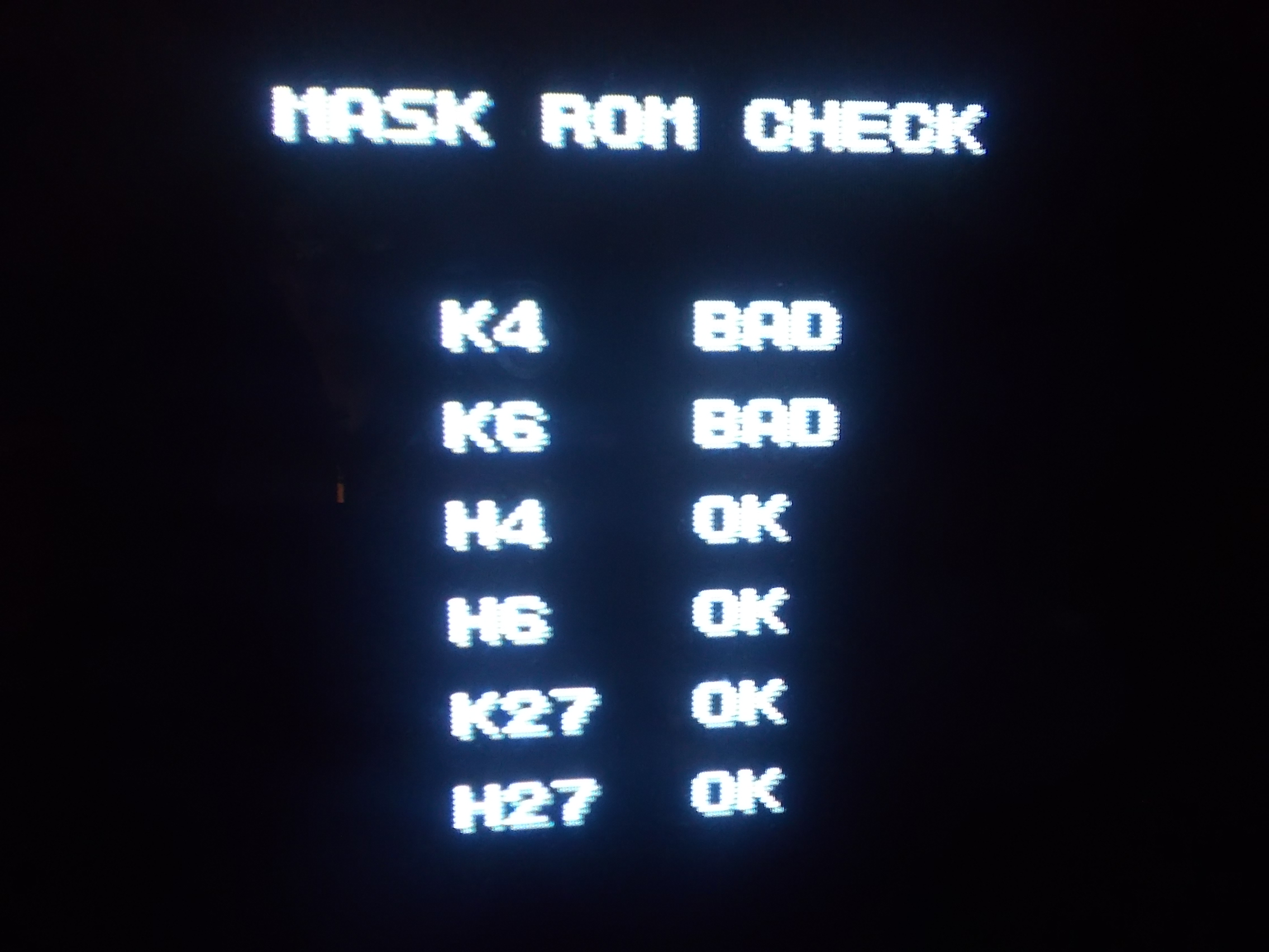
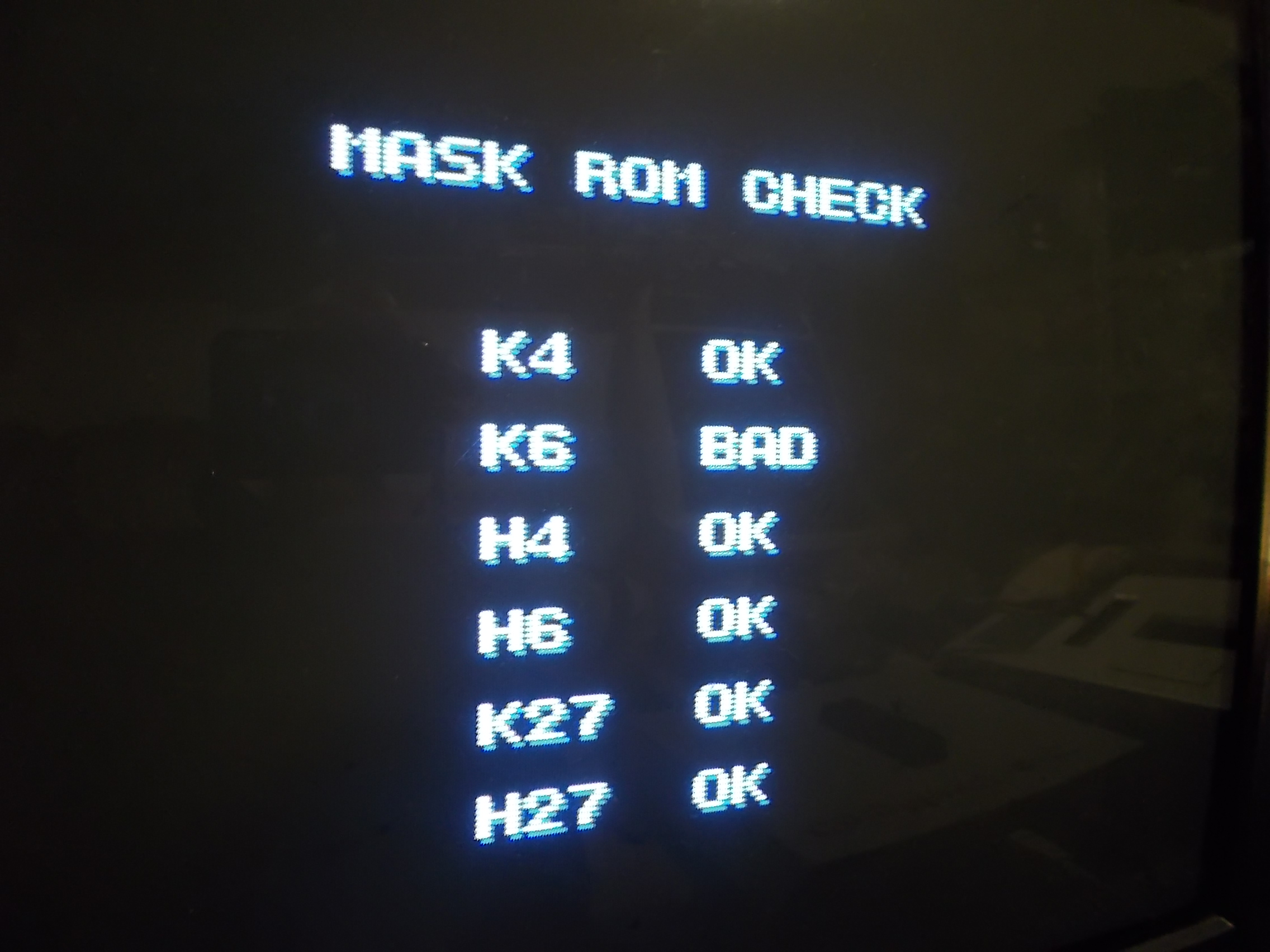
Replacing the TTL IC restored the correct colors so I moved on the grahical issues.I launched a MASK ROM check which reported two bad devices @K4 and K6:
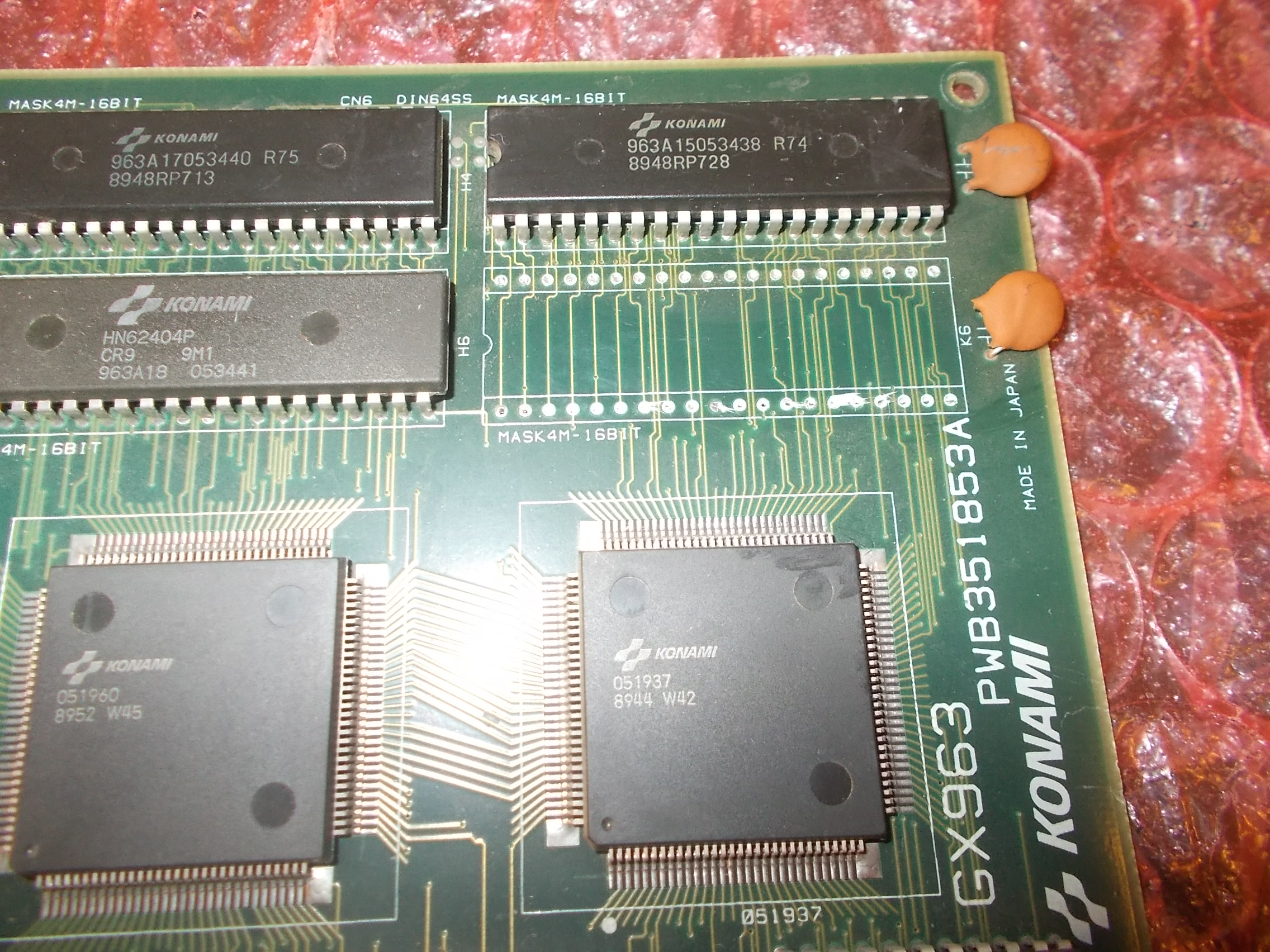
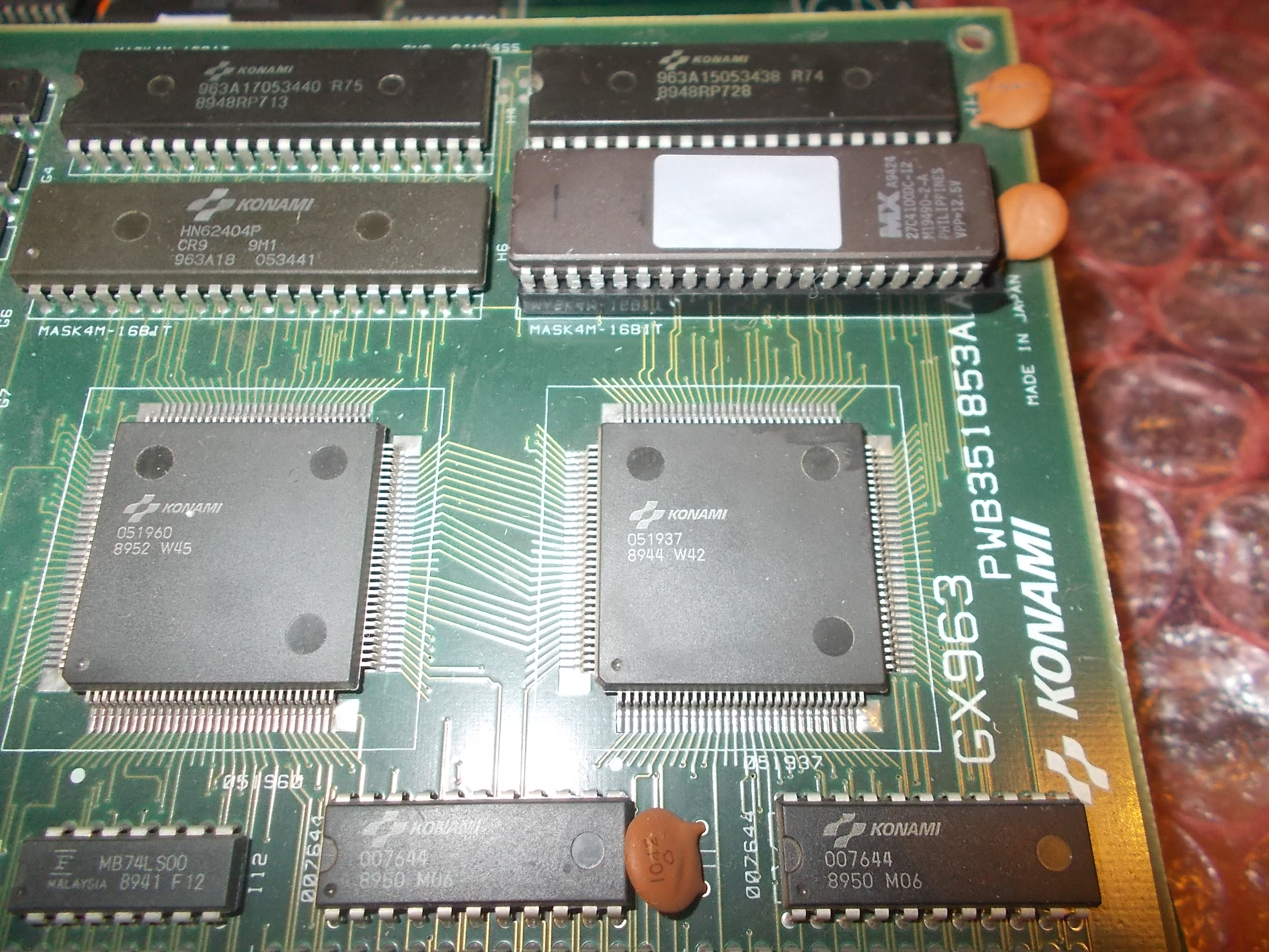
They are two of the four 4Mbit MASK ROMs that store sprites data:
I removed the first device @K6 :
I dumped it, the resulting buffer of my EPROM programmer was empty so device was really bad :
I launched again a MASK ROM check, the device @K4 was reported as good this time so the bad one @K6 was affecting it (data/address busses are shared)
I replaced the bad MASK ROM with a programmed 4Mbit EPROM (I used a Macronix MX27C4100)
Sprites were restored and check no more complained :
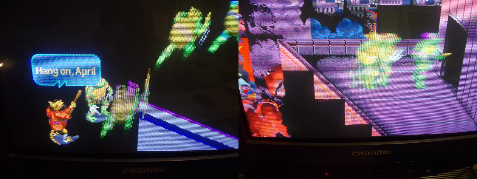
But backgrounds were still missing parts :
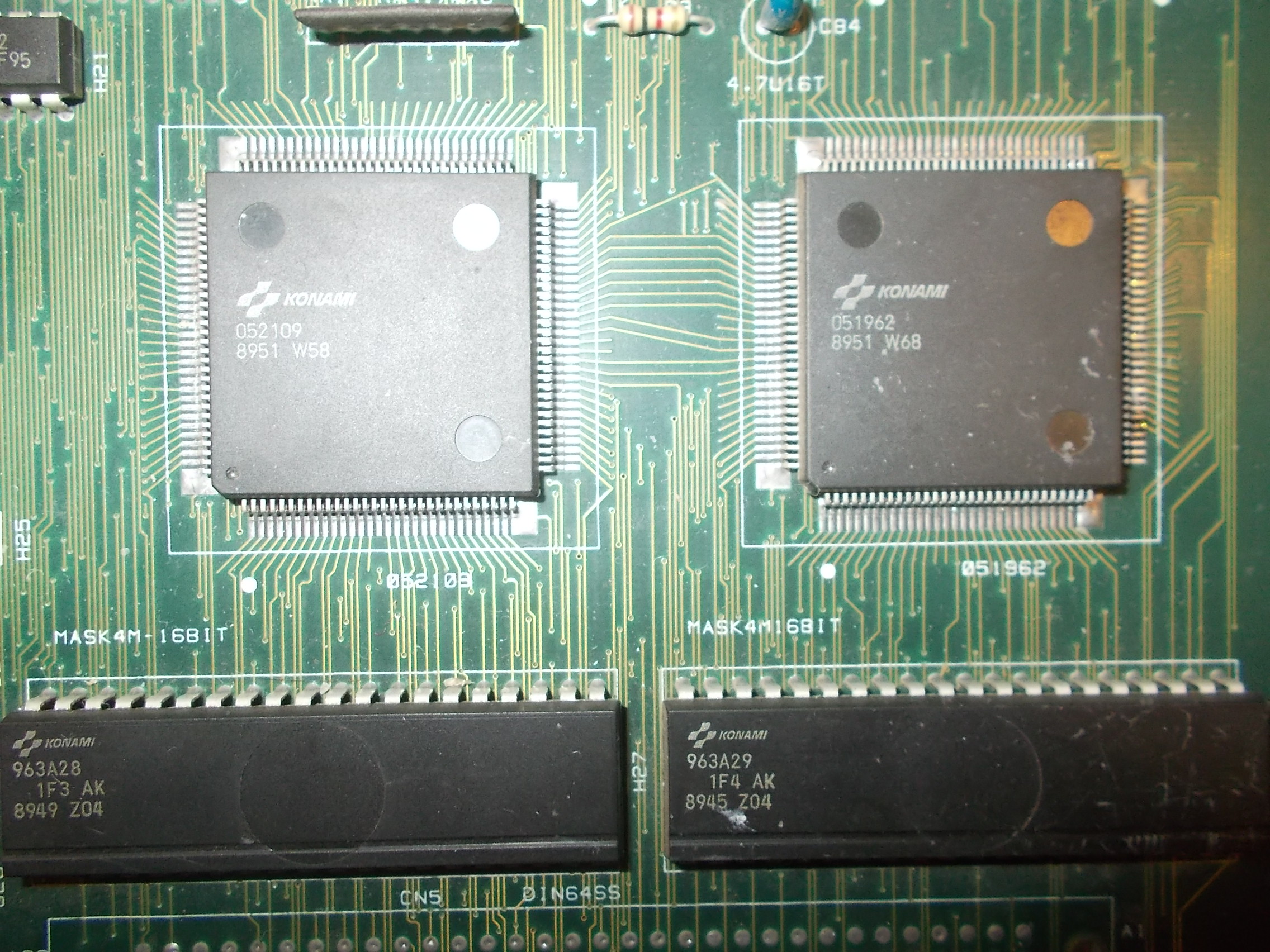
This part of graphics is entirely handled by the ‘052109’ and ‘051962’ custom ASICs:
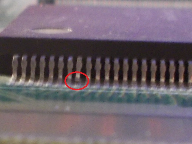
On a visual inspection I found a lifted pin on the latter:
I reflowed the pin and this fixed board completely.Repair accomplished.
I got a Megablast board that was not booting at all.
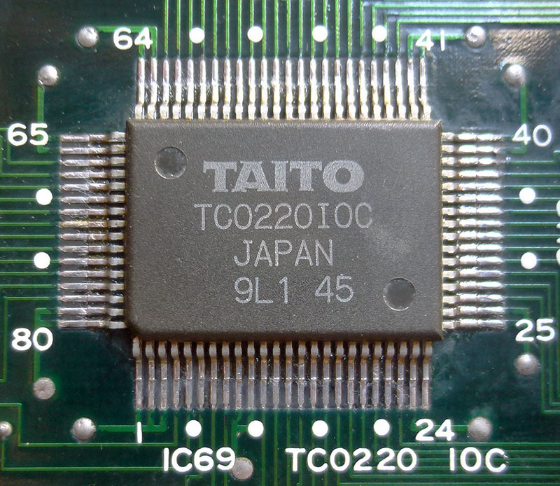
1) As reported on Caius Liquid Kids repair log (https://www.jammarcade.net/liquid-kids-double-repair-log/), it is common on these Taito F2 system boards that TC0220IOC custom chip is faulty in this case (I suspect plugging the board to the JAMMA connector upside down may fire that chip, sending it +12V via the I/O ports. That’s probably what happened here).
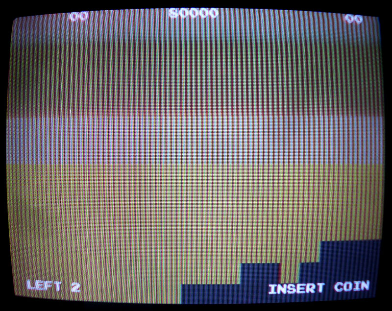
Indeed, after swapping the TC0220IOC chip from a donor board, the game booted and offered me a nice glitched screen:
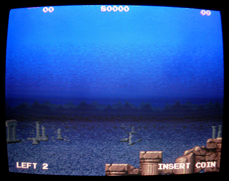
2) Another common issue on these Taito F2 boards are the mask roms getting internal disconnections within time. So I started replacing the background ROM (C11-05 @ IC58) by an equivalent 27c400 programmed EPROM and got backgrounds fixed:
3) Anyway, all the sprites were missing. After a long search and many tries I found a weak signal on one of the RAMs data line that carry sprites information between the main CPU and the sprites generator custom chip TC0200. Replacing the RAM (a TMM2063AP @ IC50) made sprites appearing, but glitched:
4) I found out that one of the sprites ROM was dead as well (C11-04 @ IC31). Replacing it with a programmed 27C400 EPROM fully restored the graphics:
5) & 6) One last thing I didn’t mentioned yet was the sound that was scratchy. More precisely, sample sounds were clearly corrupted, not the FM sounds. With no surprise, I found out that both IC where audio samples are stored (C11-01 @ IC29 and C11-02 @ IC30) were dead. Replacing them with equivalent 27c040 programmed EPROMs totally restored the sound.
Board is now fully fixed. Here is an overview of the chips I had to replace on my board (interesting fact is that Caius had to replace the exact 4 same mask ROMs on another Megablast board: https://www.jammarcade.net/megablast-repair-log/):
I recently got a few boxes non working pcbs from a friend of mine and decided to start looking at them.
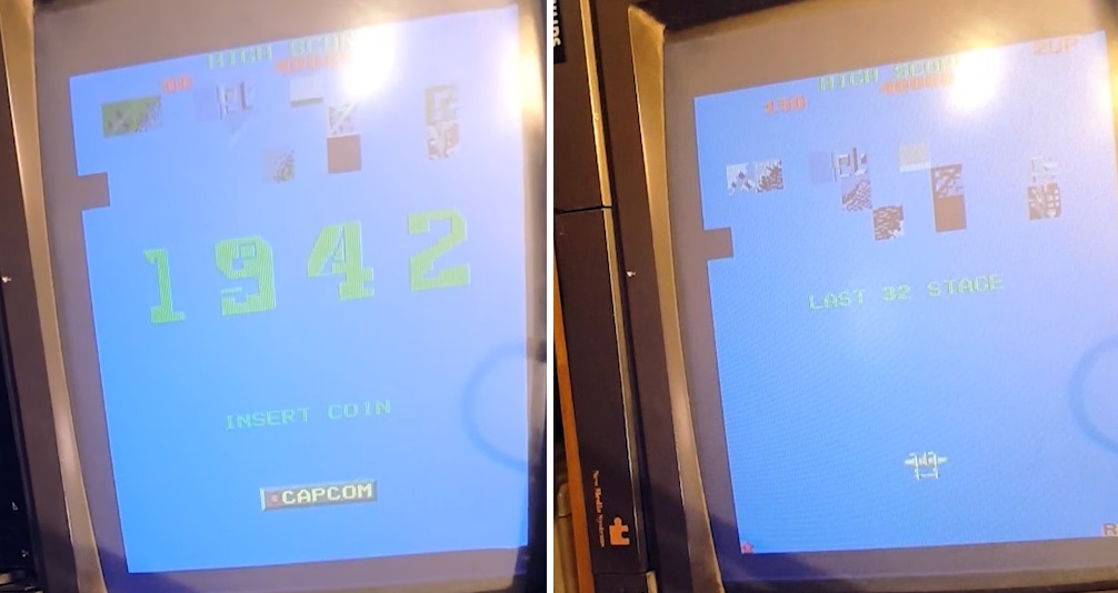
This is the first one, an original Capcom 1942 pcb.
It came with a jamma adapter so I was happy I didn’t have to spend time making one.
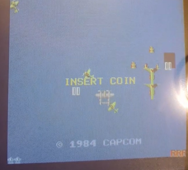
Upon starting the board, it came up as evident why it had been marked as non working
No Background layer instead showing some corrupted background
Some sprites were showing up incorrectly and only half the sprites was visible on screen
Luckily the sound was all working… for now.
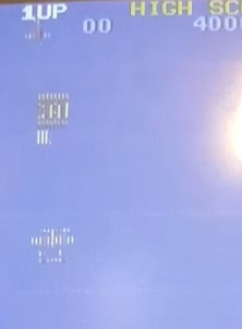
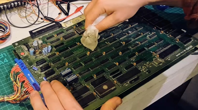
Since the board was very dusty, I went ahead and cleaned it and checked all the eproms in mame.
When putting the boards back together I quickly discovered the board ribbon connectors were corroded.
I changed those and gave the sockets and clean and now the board was booting to a much more acceptable state
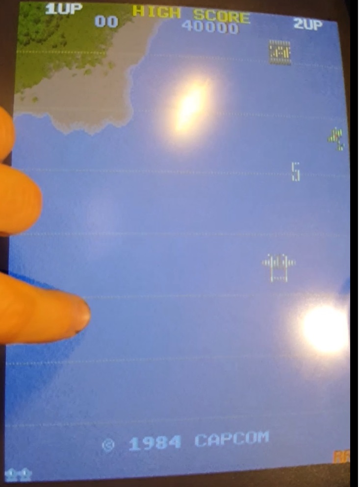
The background layer was restored but the sprites were still “halved” and showing halved white lines across the screen.
I first thought I’d address the halved sprite data.
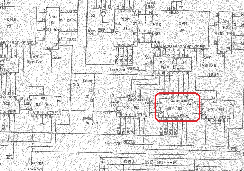
The schematics show that they are processed by two parallel identical circuits (page 16 / OBJ LINE BUFFER)
I started probing around the RAM at J4 and found Pin 15 and 14 of J6 (74ls163) were set high.
Comparing the readings from the other half of the sprite processing at F4 gave a different reading.
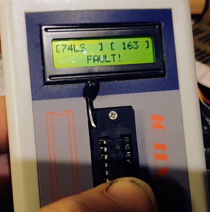
I tried to piggy back a known working ls163 and it completely restored the sprites and removed the vertical lines .
Time to remove it and socket a nice new IC. ( btw, this was a Fujitsu IC, what a surprise)
Nice ! Now to address the other sprite issue with incorrect sprites being displayed in specific segment.
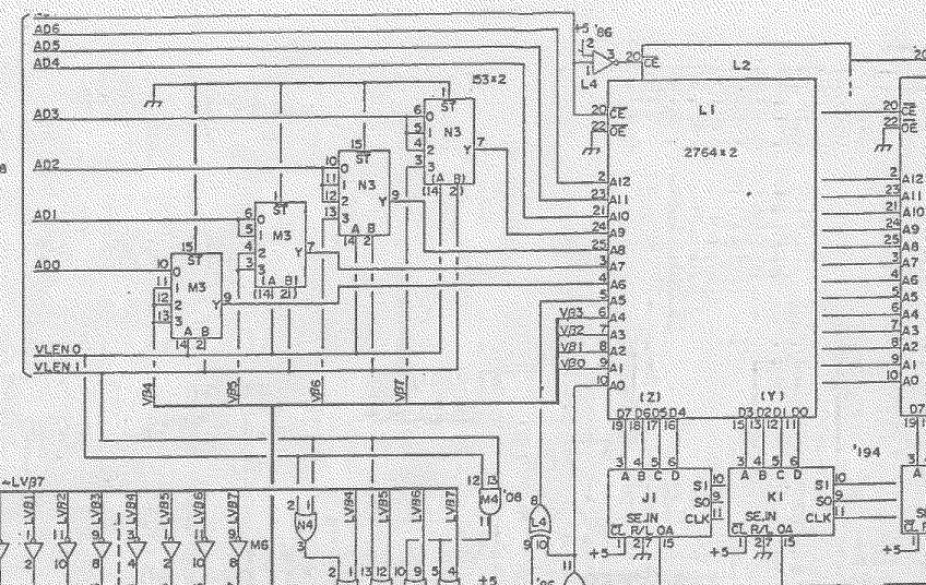
The eproms had checked fine so I reasoned this was an issue at the addressing level.I assumed that a problem on the data bus would give us random or consistently corrupted data, but here we have very valid data being used in the wrong spot.
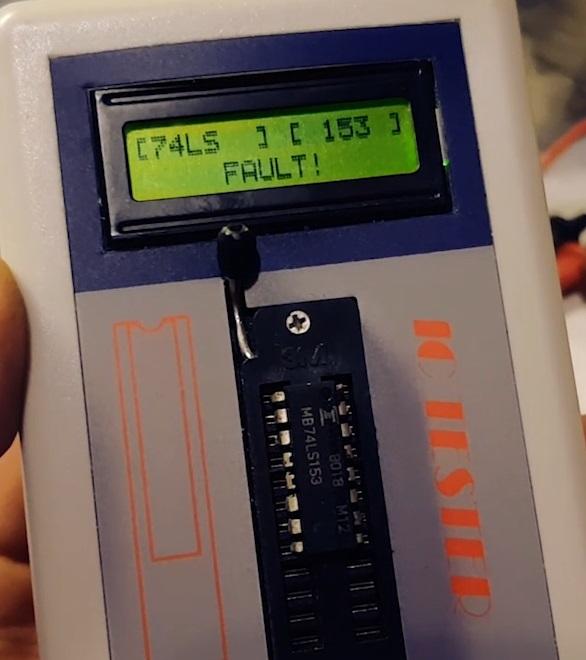
So I thought I’d start looking at the LS153 at M3 and N3. Indeed pins 7 and 9 of N3 were floating.
Replacing it completely restored all our sprites… BUT
I’ve just lost all sounds!! The entire board when silent.
While I’m full aware this can happen with boards it doesn’t mean it’s not 100% heartbreaking, especially when you thought you’d completely fixed the board.
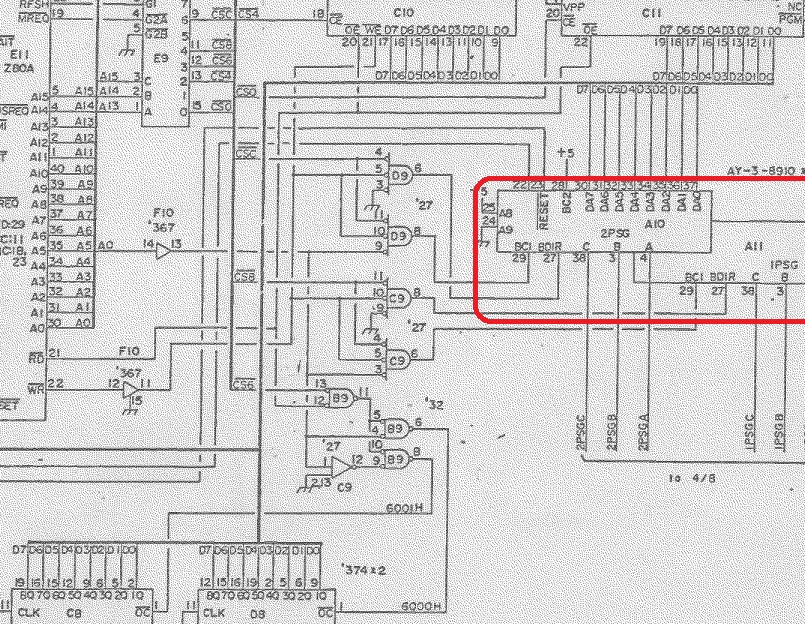
sooo looking at the schematics for the sound system at page 3 I can see this is generated by two AY-3-8910 square wave generators.
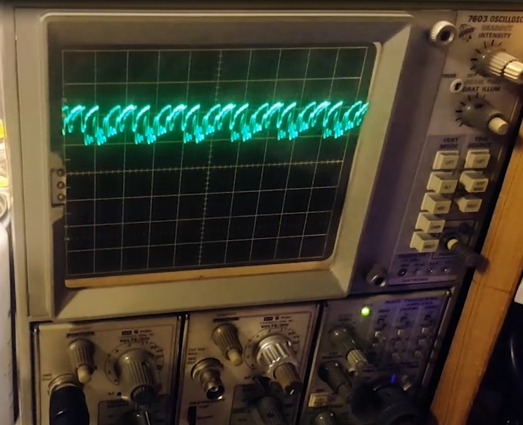
The output of both chips on pins 3,4 and 38 were completely silent. So I went ahead and re-checked the eprom first and it check fine. Looking at the data lines I could see a sort of “compressed signal” so I was wondering if sth on the data bus was causing the data levels to be that way and was preventing the sound chips from toggling high and low and thus generating the signal … maybe ?
I went ahead and removed the z80 and ram at E11 and C10 respectively but nope, they checked fine. I did the same thing with the ls374 flip-flops at C8 and D8 since these drive the sound generating events. No luck. I went on many wild goose chases with this issue and still couldn’t find anything wrong. A quick chat with Porchy and his advice was to get some sleep and leave it alone for a few days…
So I did that.
…
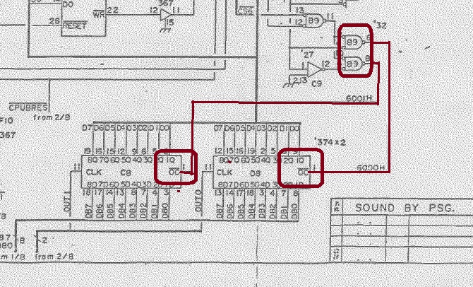
Picking this back after a week or so, I used a wire connected to ground, and driving the OE line on the ram with it, I was able to hear some sounds and music at random intervals, this meant the data lines were ok and could trigger the sound ICs. So I moved away from the Z80 section of the circuit and that the issue was most likely with the chip enabling section of the circuit so I started looking at the ICs driving the enable lines.
I checked D9, C9 and B9 but all the signals seemed healthy on the scope. Comparing this with a known working board I couldn’t seen anything jumping out at me. This is where I wish I had a proper logic analyser but at least I felt I was on the right path. But still I had a feeling I was looking at the right area, I started removing and testing D9, C9 (mental note: invest in a logic comparator) and then finally B9 which tested faulty
The last IC on that entire sound circuit !!
Looking back at the circuit it makes sense, this IC enables the output control of the LS374 driving the event data into the sound circuit. Without this, the sound circuit doesn’t “know” it’s supposed to generate a sound.
Replacing it restored all the sound circuit .
Board all fixed, and lessons learned:
Sometimes getting some sleep and leaving a board alone for a while is best
Always check the enable lines first
… and start looking into getting a logic analyser.
PCB Repair LogsComments Off on Hammerin’ Harry (Irem M81) repair log
Apr182019
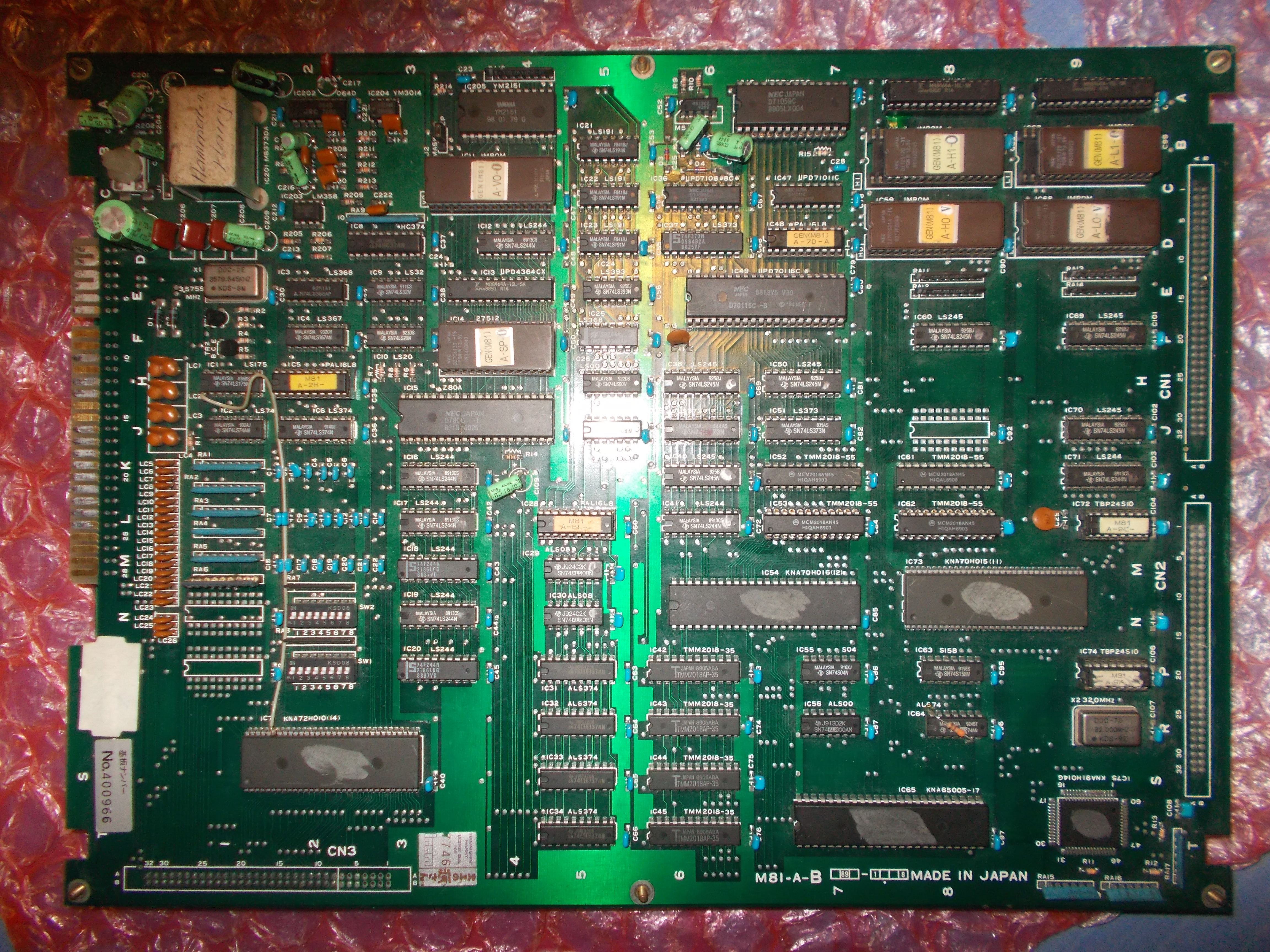
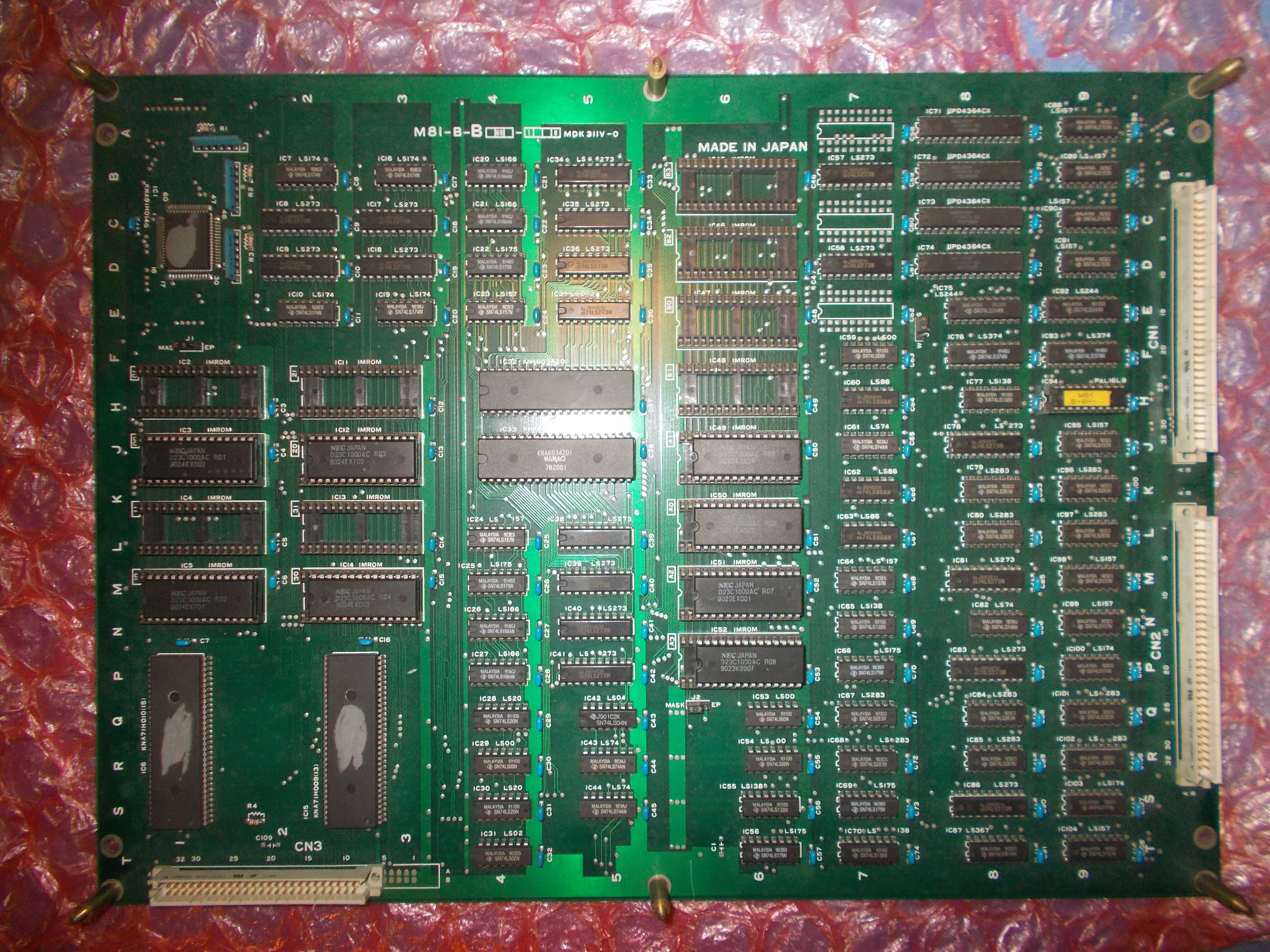
Received for repair an Hammerin’ Harry PCB on Irem M81 hardware (it can be found also on M84).
Set is made of a top CPU board:
And a bottom VIDEO board:
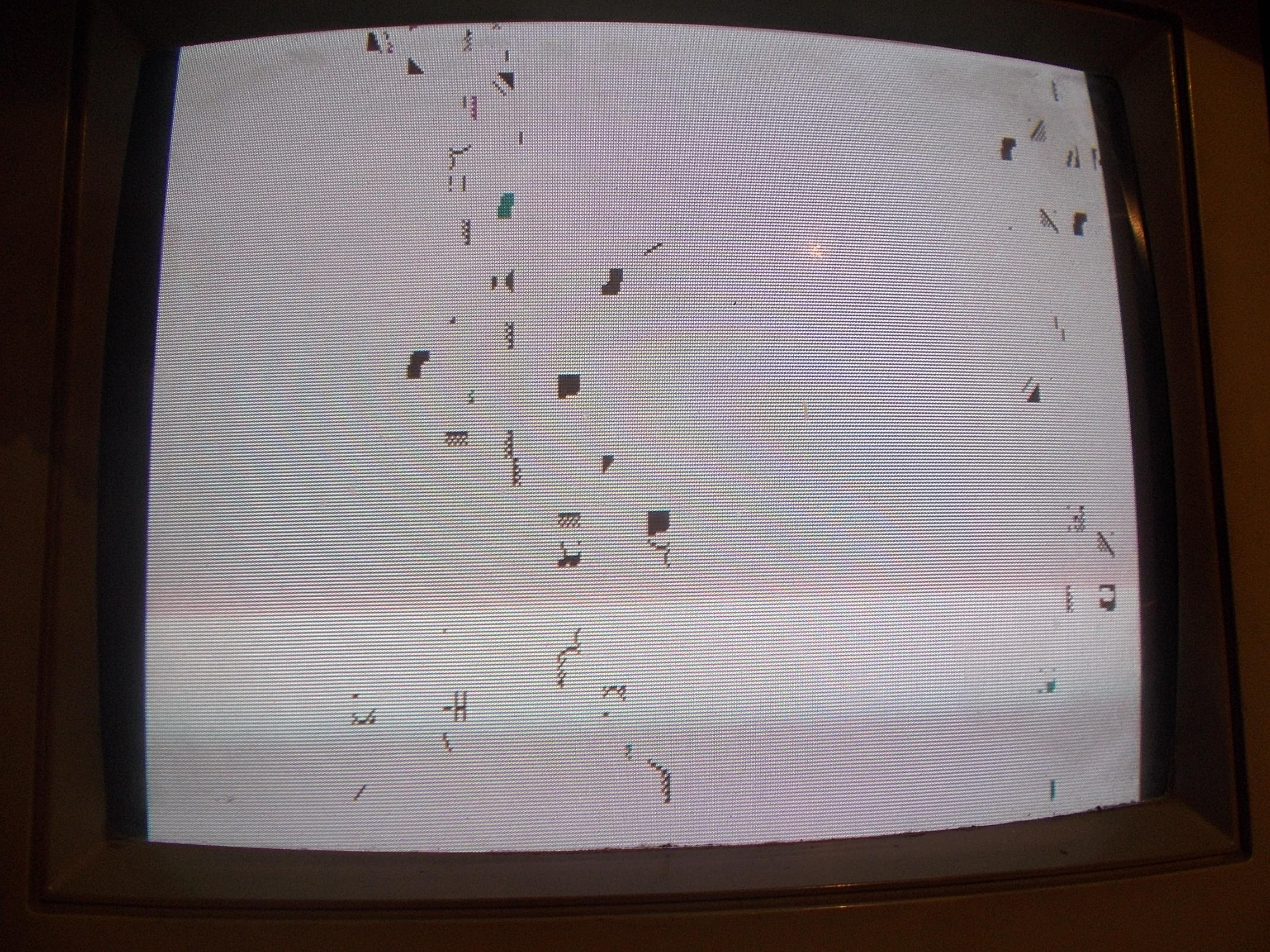
The PCB simply booted to a static garbage screen:
The NEC V30 (uPD70116) main CPU was active on its data/address busses but when I probed the program ROMs I found a couple of stuck address lines :
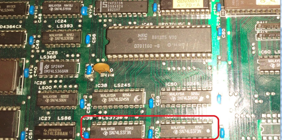
Looking at hardware I figured out there are some 74LS373 used as latches to address the program ROMs :
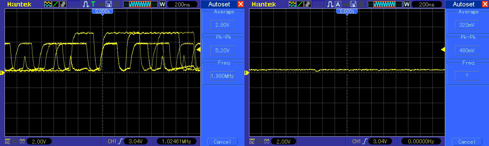
Probing the one @IC39 revealed some outputs were floating while inputs toggling:
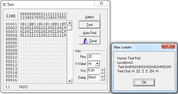
Once removed the chip failed the out-of-circuit testing :
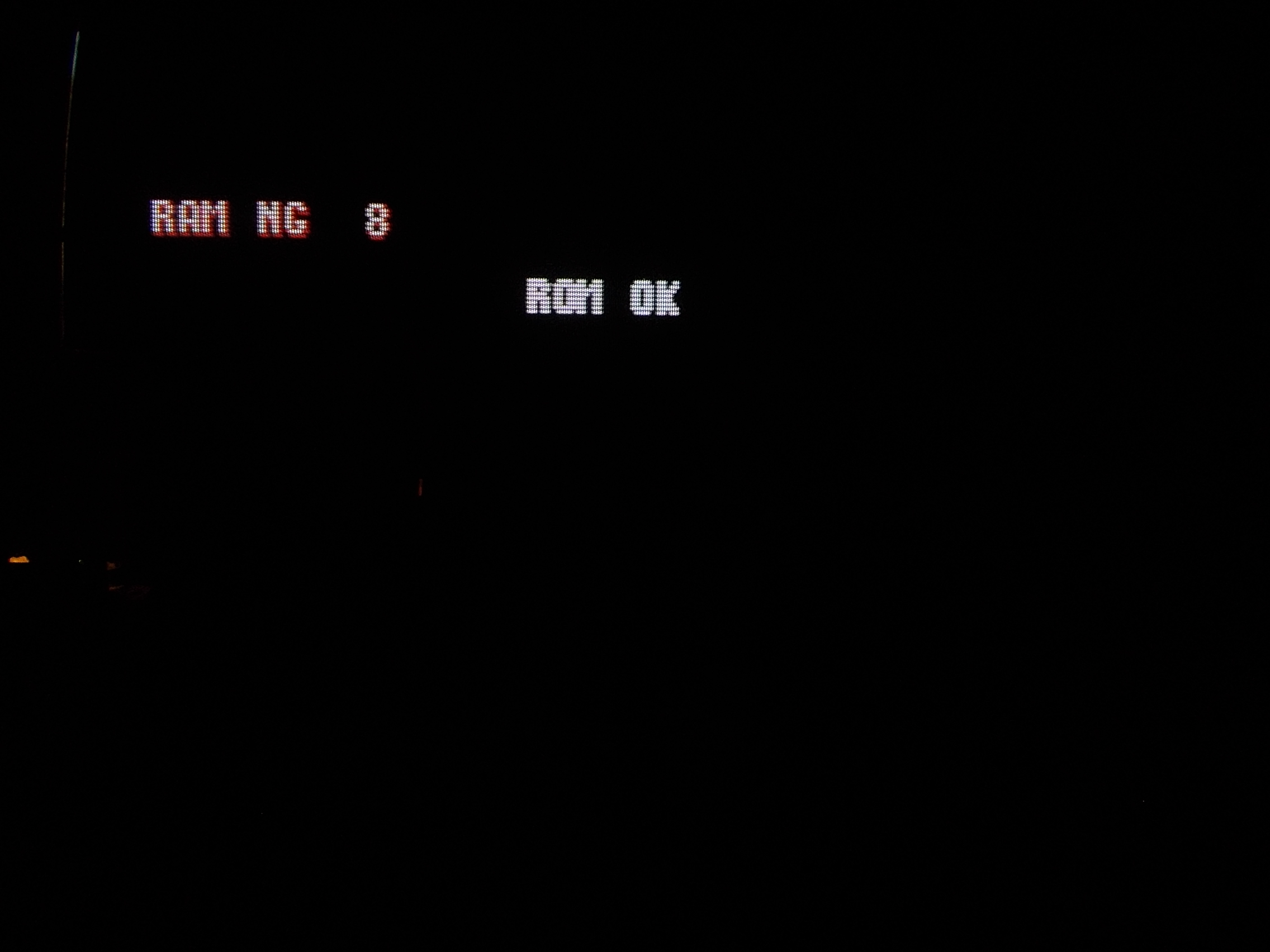
I replaced the chip and the board booted up but on self-test showed most of times a ‘RAM NG 8’ message:
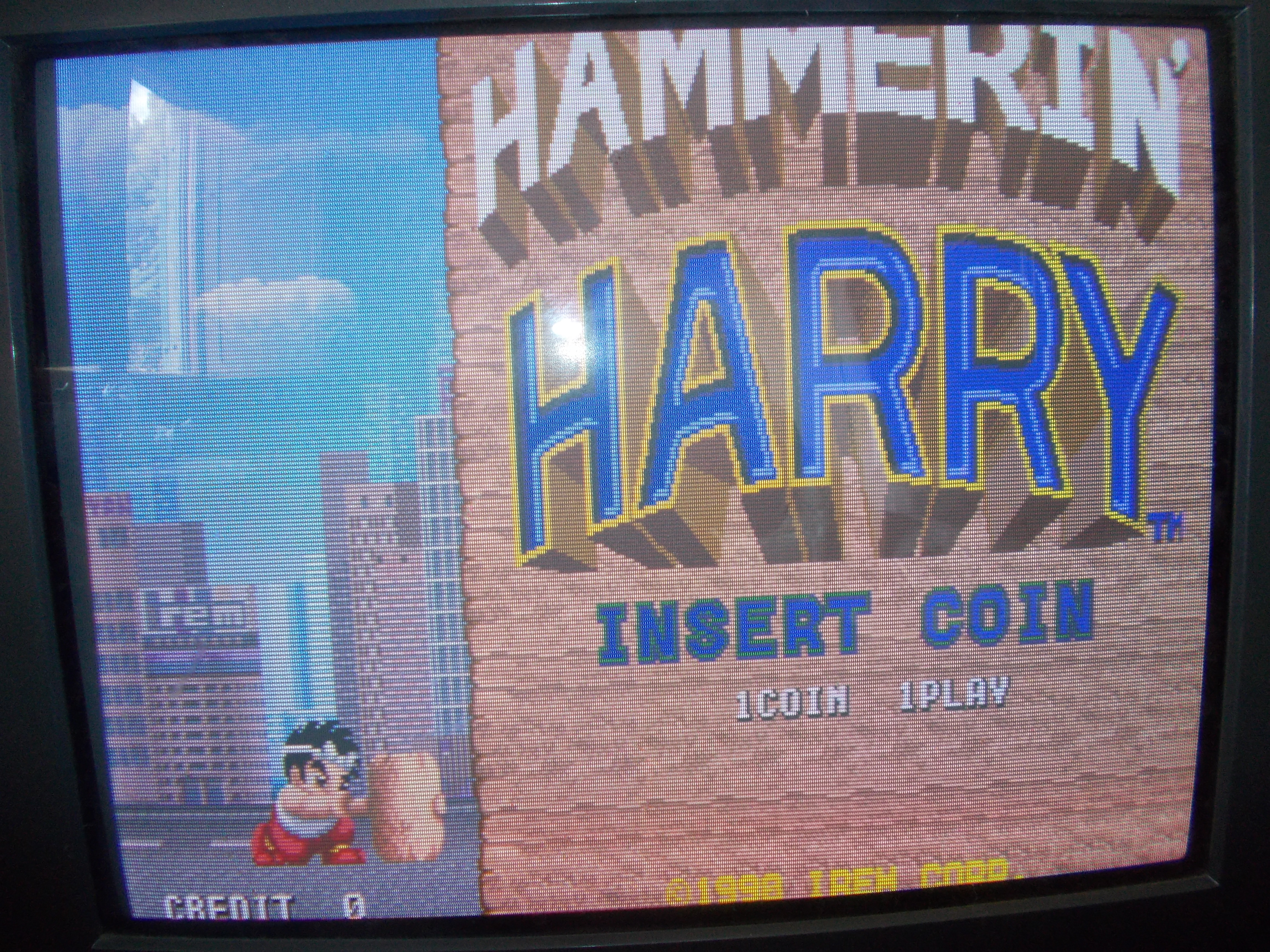
Then it entered in game which was playable with sound but background colors were wrong :
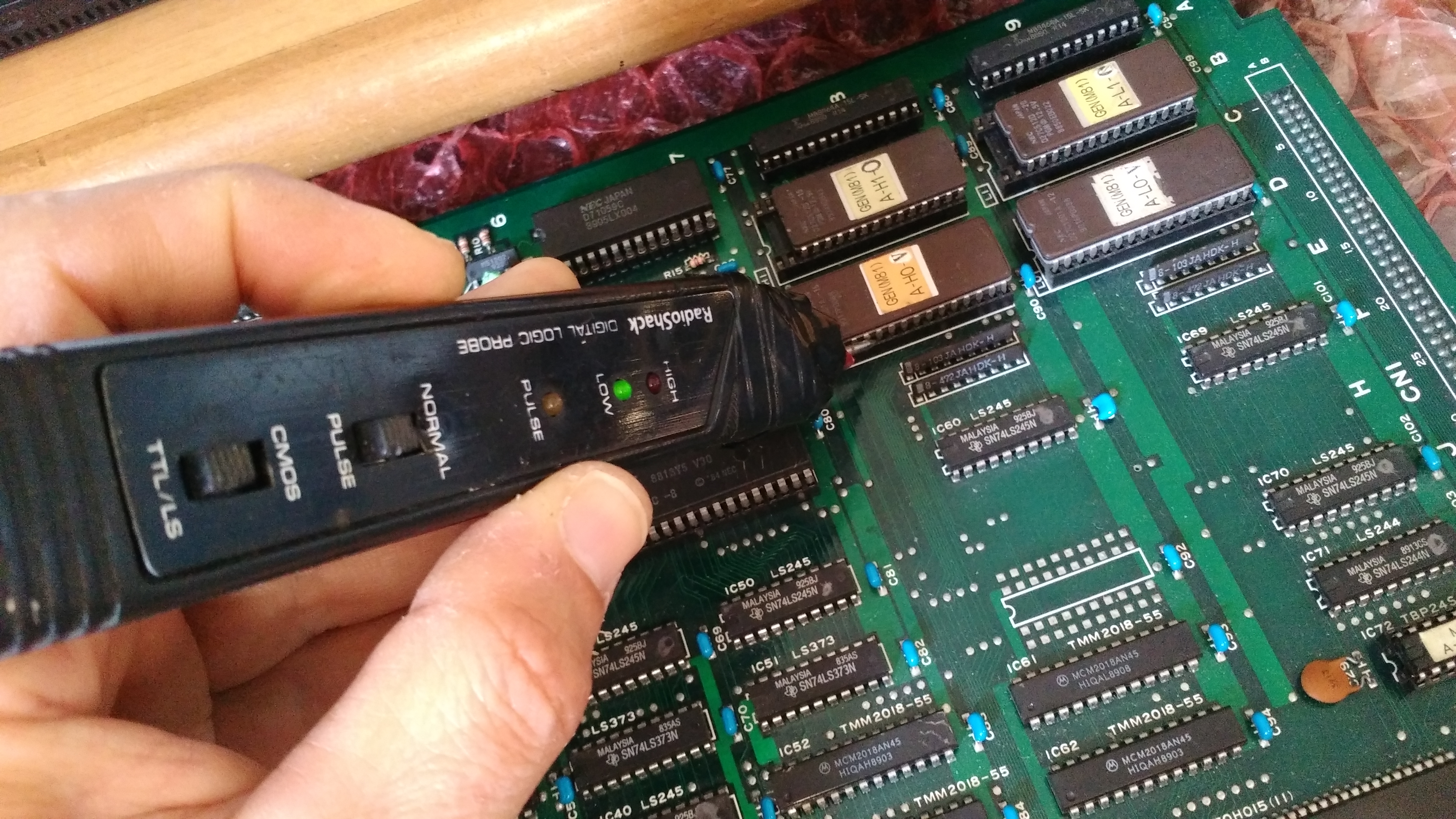
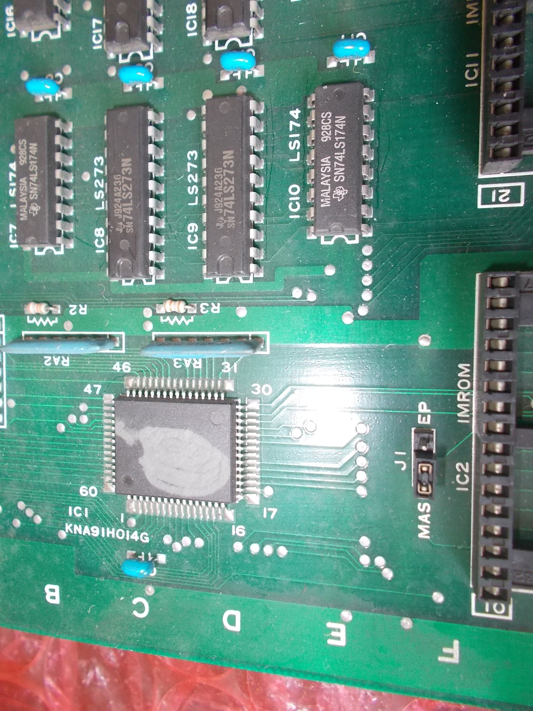
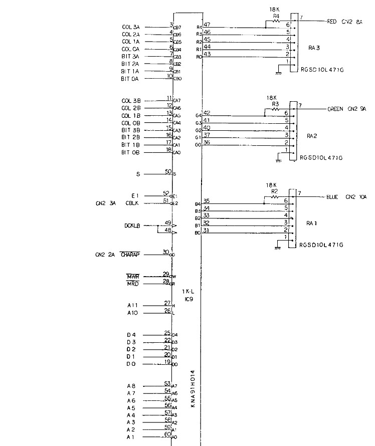
The ‘KNA91H014’ surface mounted IC on bottom board @IC1 generates the palette for this part of graphics:
Its pinout/implementation from R-Type schematics :
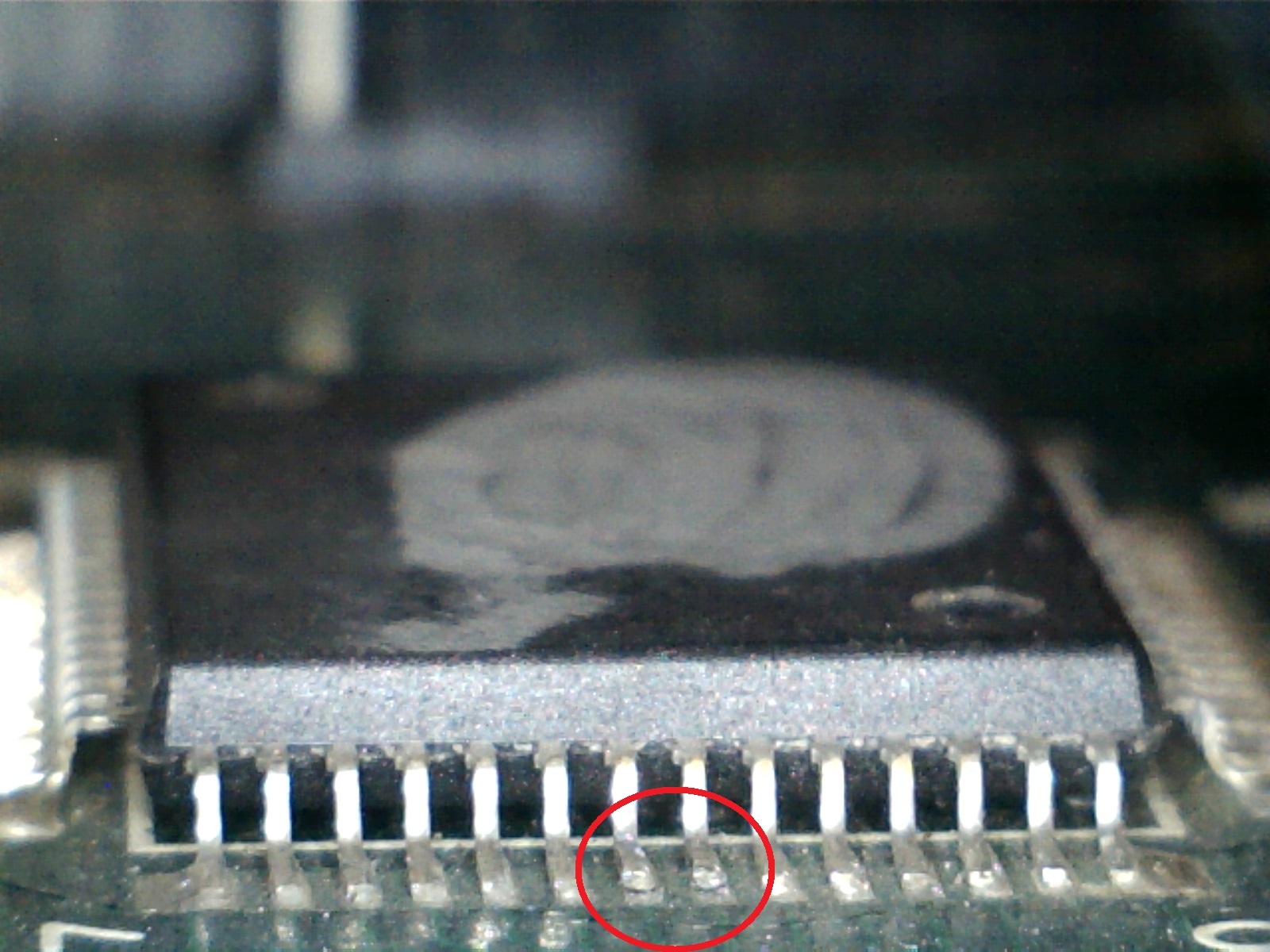
I made a visual inspection and found a couple of lifted pins on a row:
I reflowed the whole IC with result that self-test no longer complained and graphics were fully restored:
The last issue I had is that some inputs were not wotking but I quickly pinpointed it to a missing custom resistor array near the JAMMA edge connector:
Having no spare I replaced it with a reproduction of mine:
PCB Repair LogsComments Off on Scramble (bootleg) repair log
Apr092019
Hammy sent me a couple of boxes of PCB’s recently. Among them was this Scramble bootleg PCB.
I’m still not sure if this pinout is unique but I had to figure this one out for myself.
Finding the VCC and GND pins is easy enough and just a matter of checking continuity from a know IC.
Once I had the power pins hooked up I fired it up and used the scope to probe for video signals. As long as the board boots the RGB should be easy to identify and as long as sync is being generated we should be able to find a 15khz signal somewhere.
Fortunately for me that is exactly what I found so I hooked them up and got this
I already knew this game didn’t match anything in MAME but I pulled all the ROM’s anyway and dumped them.
The Z80 is socketed on this PCB so I plugged the Fluke 9010 in and carried out the ROM tests. All the ROM’s could be read without a problem.
Next on to the RAM.
I originally looked at the wrong MAME source for this board. I looked at galaxian.cpp but I should have been referring to galaxold.cpp. Because of this error I ended up wasting a bit of time looking for a fault that didnt exist.
One this PCB the work RAM is between addresses $4000 – $47ff.
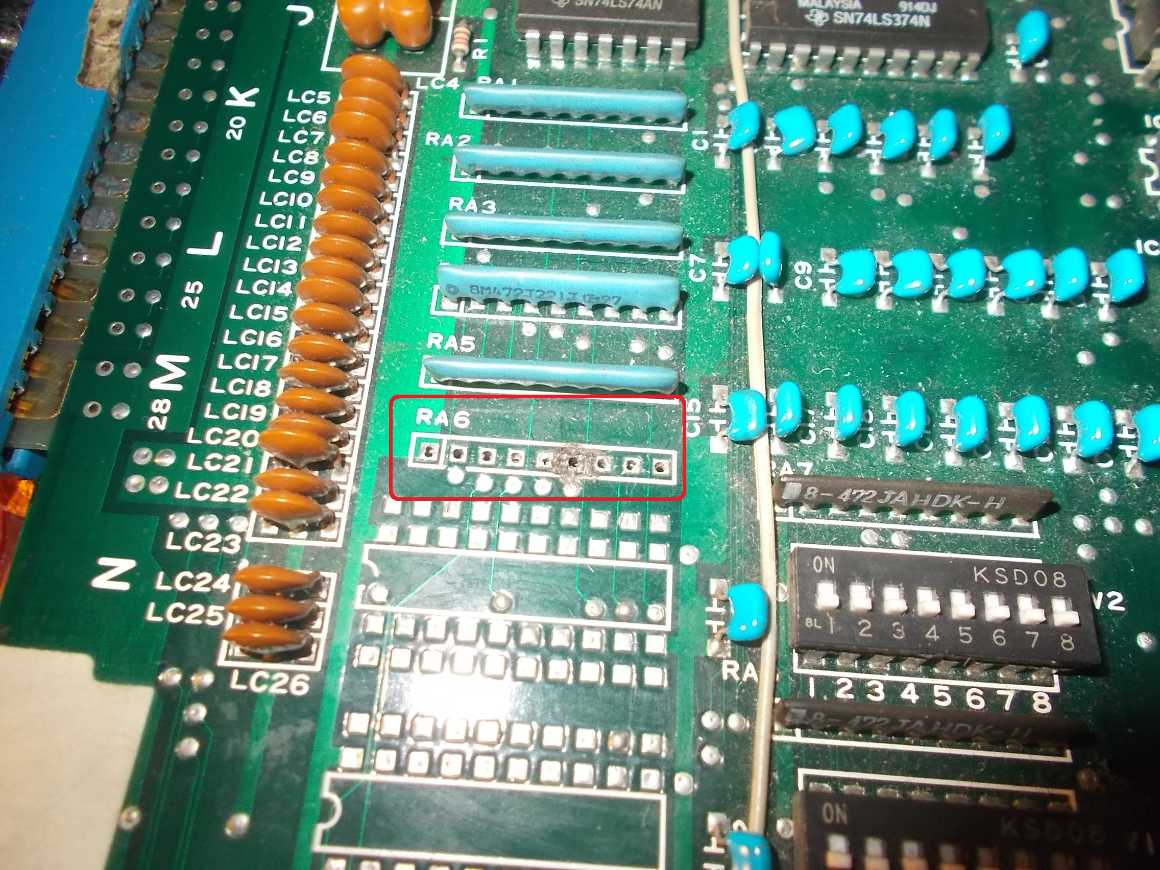
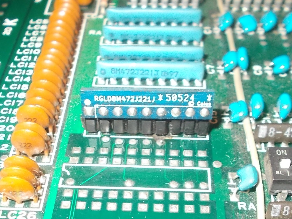
On the riser PCB I could see 2 x 2114 RAM’s which are a 4 bit memory but this would only give me 1024 (0x3ff)bytes on RAM and I was expecting double that. Removing the riser board revealed the second set of 2114 chips.
Running the RAM check on the Fluke gave me RAM errors in the upper half of the range which I determined was on the riser PCB. I removed both of them to be sure and found one was giving errors on 2 address pins
Replacing this gave me this
Error 3 doesn’t exactly give me much to work with so I just went round the other RAM ranges. There is some screen RAM at address range $5000 – $50ff. This failed.
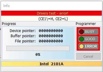
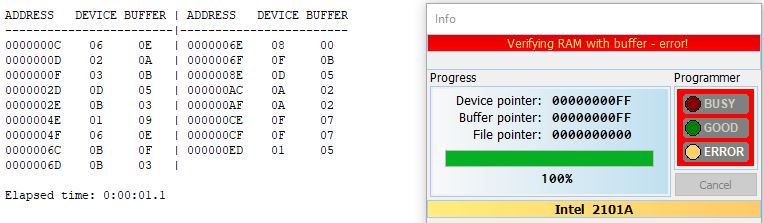
This RAM in 2 x 2101 and as luck would have it it is already socketed.
I removed both and tested them and both failed
I have plenty of these spare due to my dealings with early Nintendo boards so swapped them right out.
We have success and with the audio hooked up we get this.
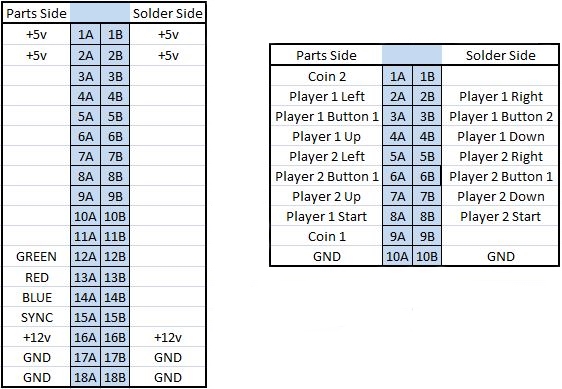
The riser board on this thing seems to be for the control inputs
Here is the pinouts I got for the PCB. There is likely a few things missing like coin counter but I’m not bothered about that.