My friend Josef sent me some boards for a repair and among them there was this Vulcan Venture (export release of Gradius II – GOFER no Yabou) :
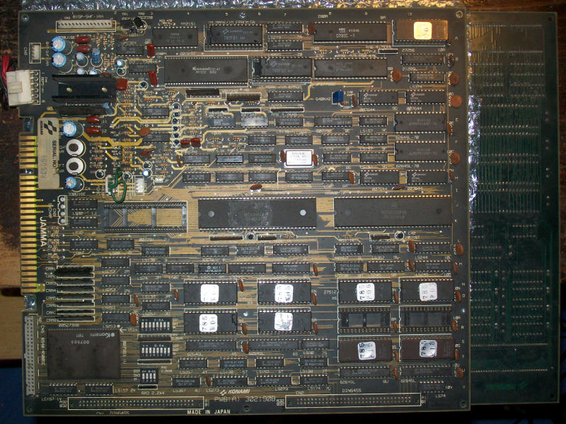
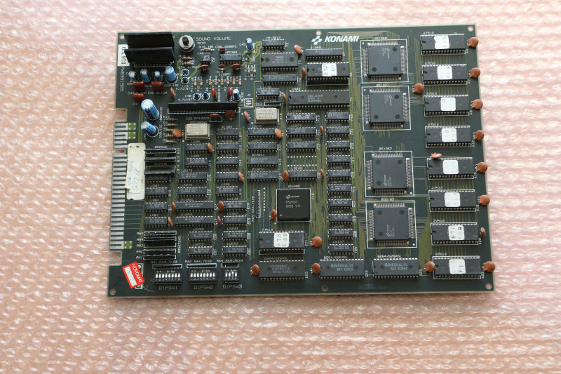
This Konami hardware ( called Twin 16) is as beautiful as complex : two 68000 CPUs, one Z80 as sound CPU (Yamaha 2151 + YM3012 DAC, UPD7759C and a 007232 Konami Custom Chip as sound chips).Specifically video board use a lot of custom chips whose functions are not really documented.With this in mind I began my troubleshooting and fired the PCB up:
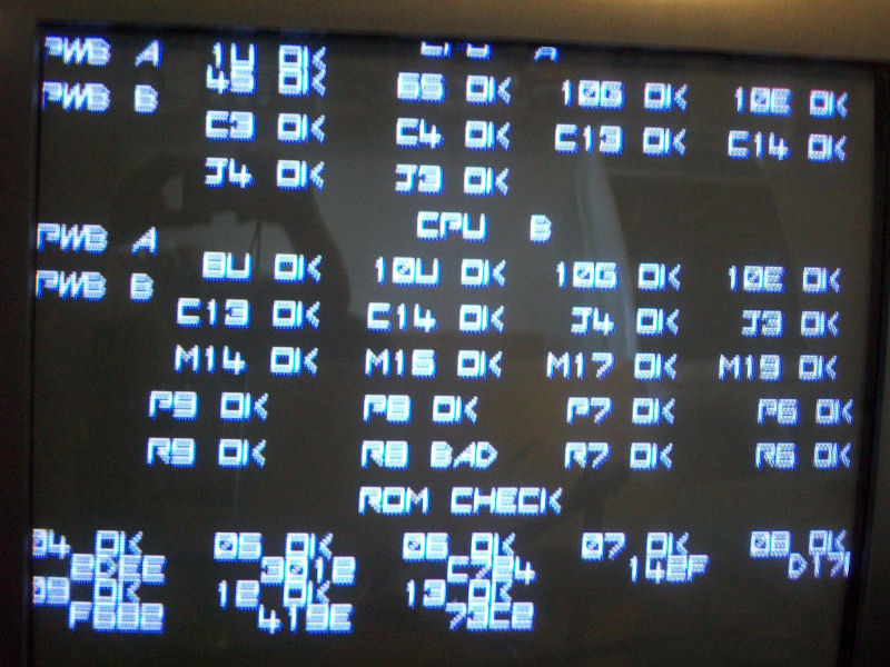
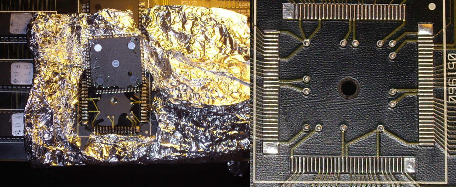
Initial RAM/ROM self test reported a bad RAM @R8, this is located on video board in form of a MB81464 chip (a dynamic 64K x 4 bit RAM, there are eight of them in this section)

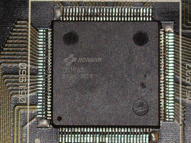
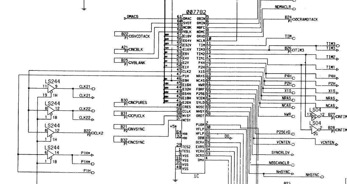
I was very confident that this would have been an easy repair but I was tremendously wrong because, after replacing this RAM, the board died.I couln’t get anything on screen but only some flashing lines and sometimes I could barely recognize the “RAM ROM CHECK” message.Sadly schematics of this board are not available so you have to seatlle with the Dark Adventure ones which runs on same hardware but has different ICs location.The fault was located on video board since, as I said, board properly booted but it played ‘blind’.In particular looking at Dark Adventure schematics I noticed that the custom marked ‘007782’ generates some video timing signals:
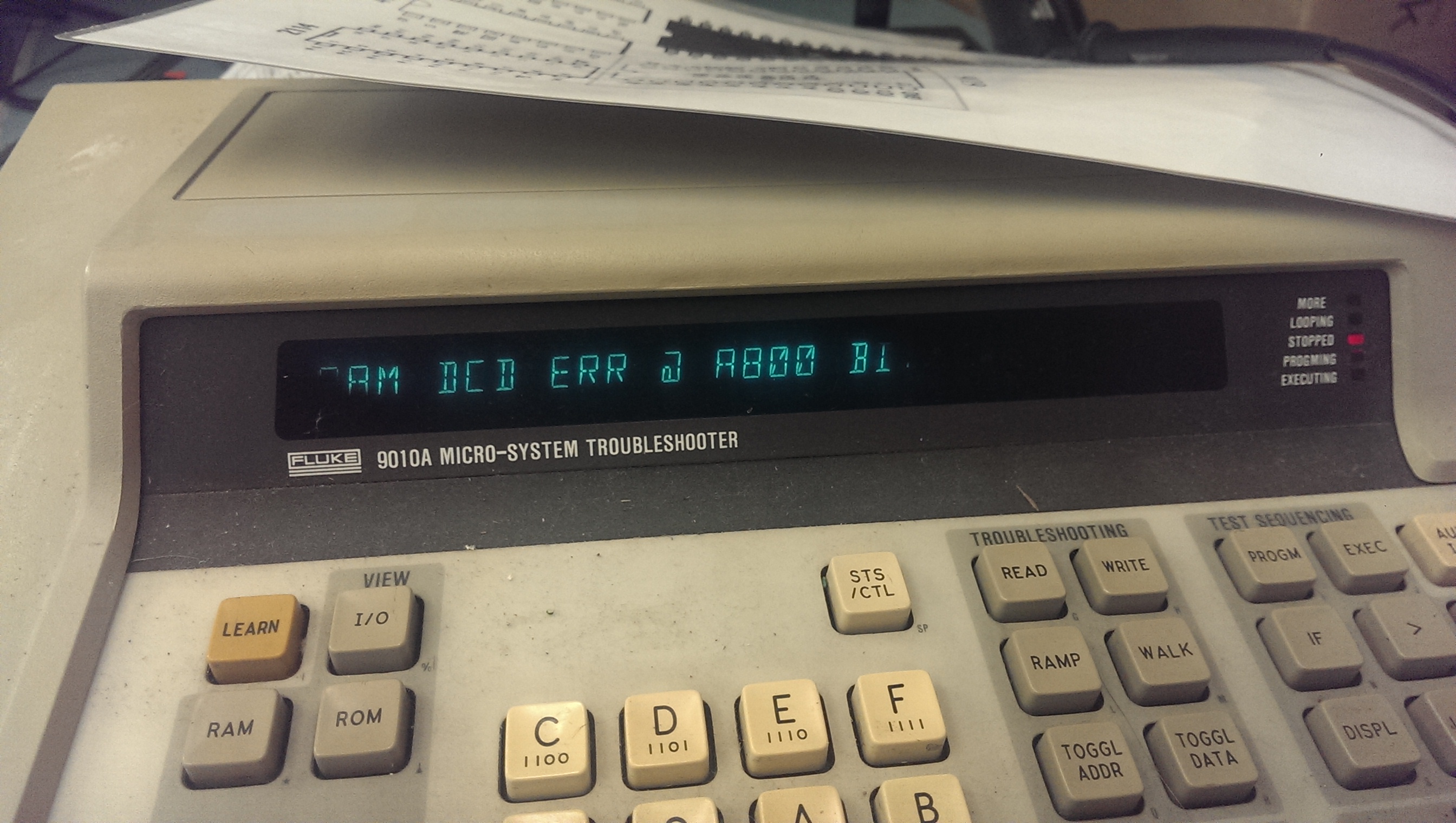
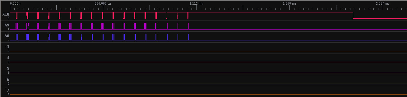
So, given the typology of my issue, I started to check this part of circuit.All signal from the custom were fine but when I piggybacked the near 74LS244 @A4 the video output was restored.I fired up my logic analyzer which gave me this result on some gates:
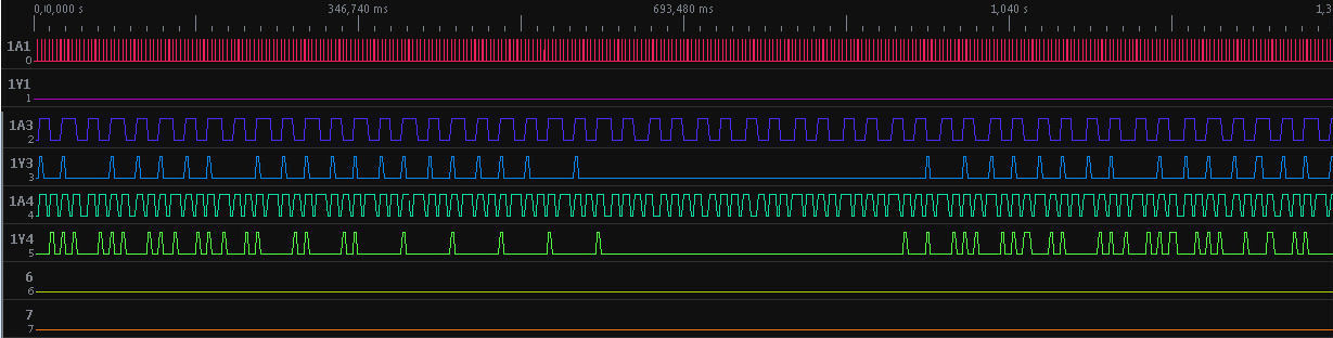
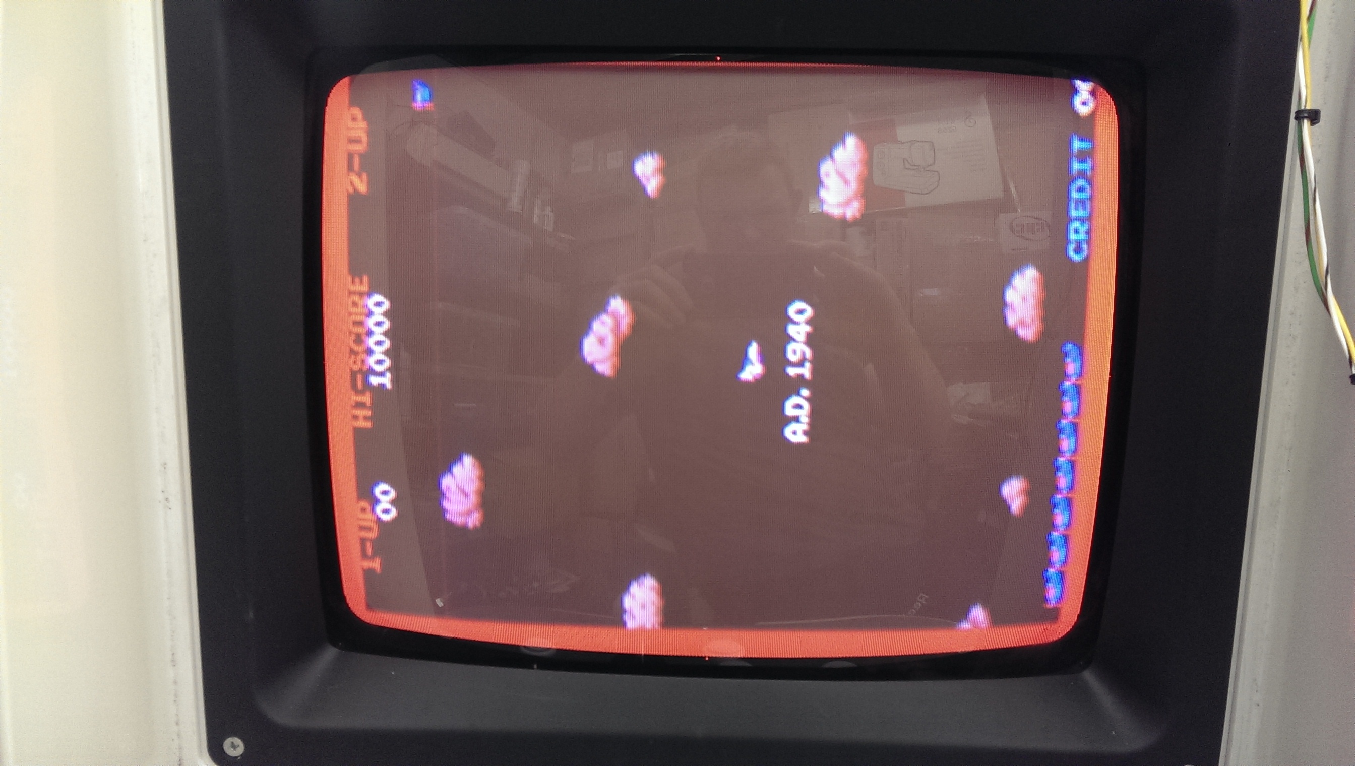
As you can see output signals were absent (like in gate A1/Y1) or altered.Tested out of circuit, this 74LS244 failed miserably.Replaced it, board booted and displayed properly but was stuck on “RAM ROM CHECK” message.Analysing the CPU board revealed that 68000 sub CPU has /HALT line active so something was wrong in its bus preventing the proper execution of code.Also here the old but effective piggybacking technique came in help since since when applied it to a 74LS244 @10L (which, indeed, sits in the middle of the address bus of the 68000 sub CPU and its work ram) I could enter in game:
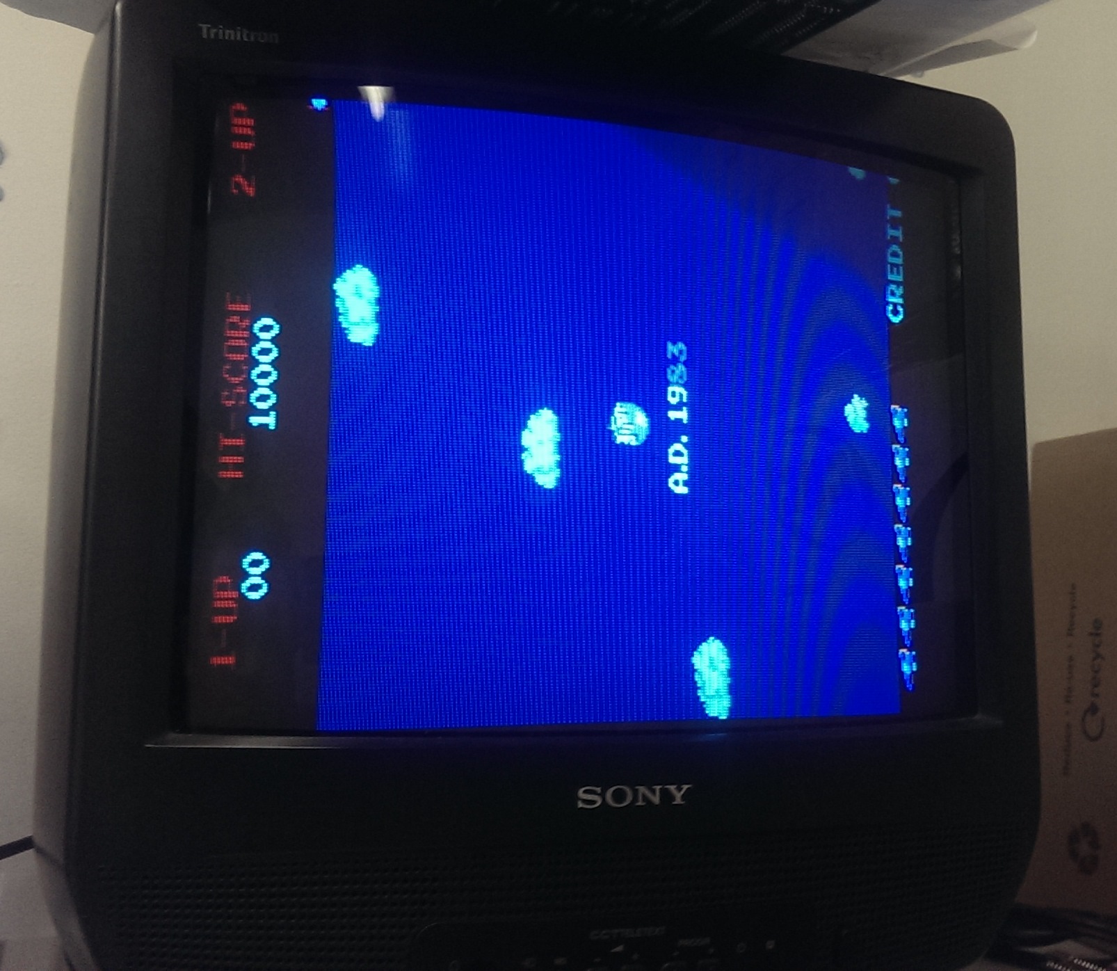
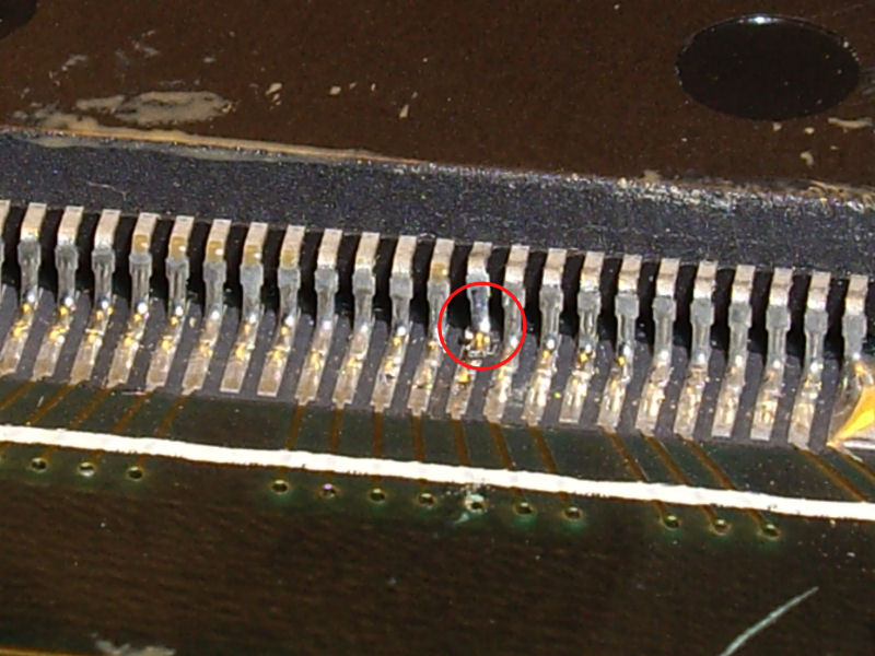
Gameplay was fine but background graphics were constantly rolling (besides, some of the audio PCM samples were garbled).I was pretty sure this fault was in the same location of the first one (around the custom ‘007782’ area).Looking at this part of circuit I noticed a small 220 pF ceramic capacitor soldered across ground and PIN15 (input) of a 74LS244 @A10:
Usually little ceramic capacitors are used to clean signals filtering them.In this case the signal to this input of the 7LS244 came from the custom ‘007782’ and was called ‘NRAS’ on schematics while the corrispective output was connected to the RAS line (row address strobe) of the eight MB81464 DRAMs previously mentioned (they are used for tilemaps).Also here piggybacking this TTL , after removed the capacitor, cleared the issue ( actually this 74LS244 was tested as good in all my programmers but does not mean its internal junctions were fine).I was going to analyse the sound issue but board developed a new graphics issue :

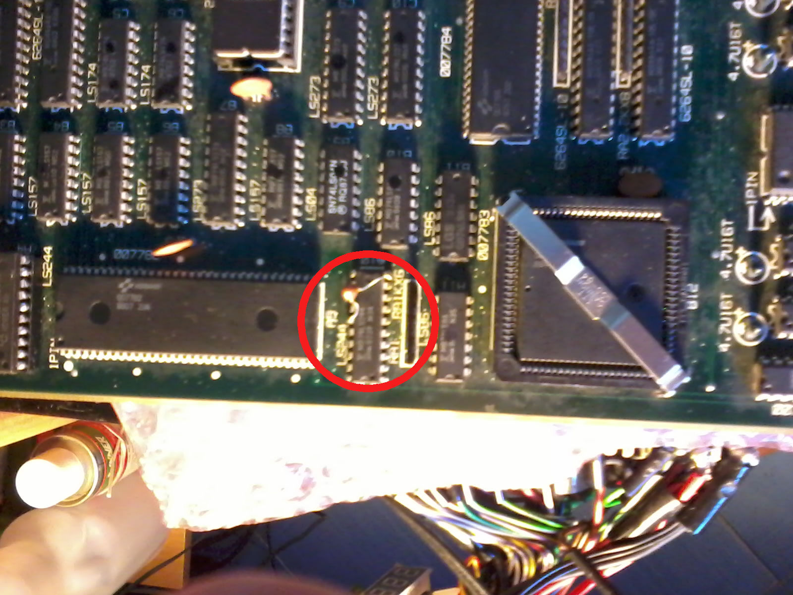
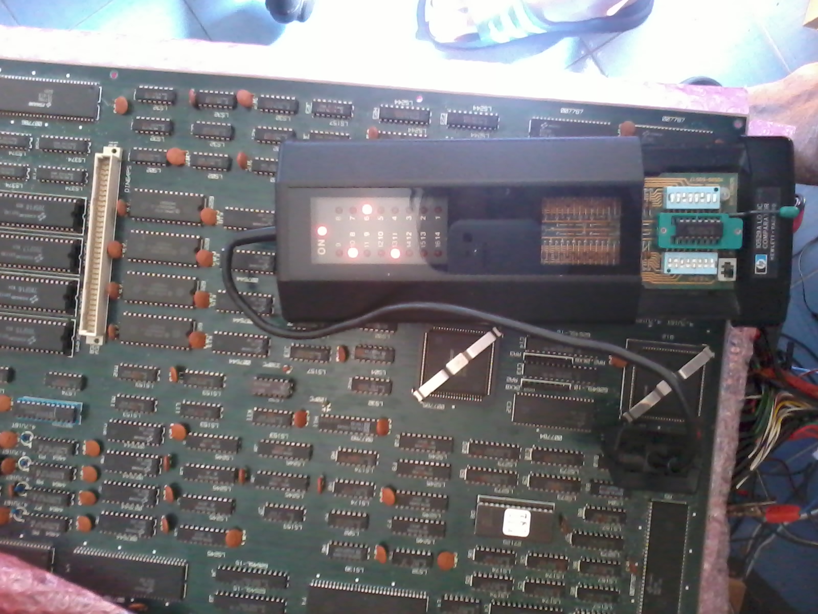
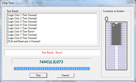
Text/characters were all blocky but I could quickly pinpoint this fault in a bad 74LS86 @B11 on video board using my HP10529A logic comparator:
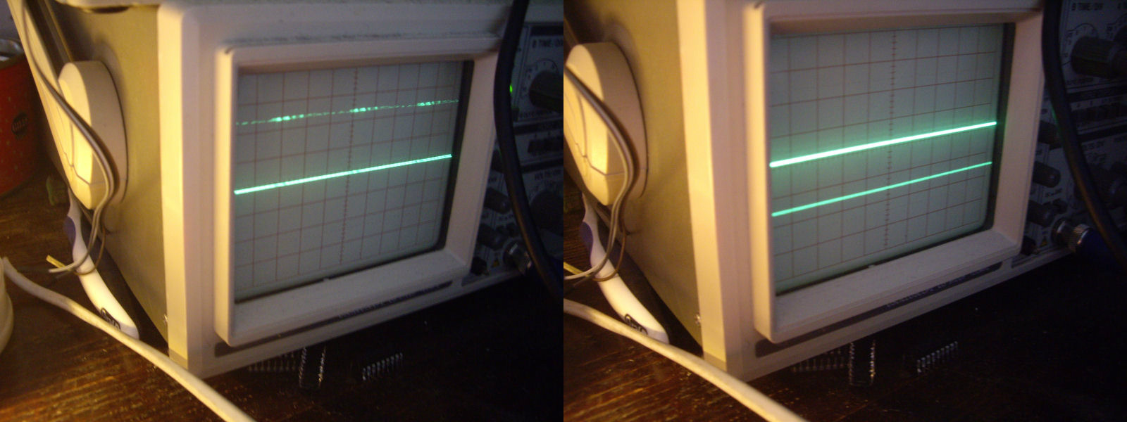
So, now graphics were completely restored, it remained to be fixed only the sound.Sound hardware is made of a main Z80 as CPU , a Yamaha 2151 + YM3012 DAC, UPD7759C and a 007232 Konami Custom Chip as sound chips.Music was fine but some of the PCM samples (speeches) were garbled.For example the initial speech “DESTROY THEM ALL!” was played so :
while the correct should be:
Studying a bit the hardware with the help of The Main Event schematics and doing some tracing on the PCB, I could figure out that the MASK ROM containing speech samples is addressed by the NEC D7759C chip not directly but through a 74LS273 @7B (while the ‘007232’ PCM custom chip addresses the other samples MASK ROM). Probing this ROM I found that most of its address line were stuck LOW or HIGH.I dumped it and it matched the one in the MAME ROMset.So, at this point fault had to lie in 74LS273 @7B that was in the middle of address bus.Without thinking twice I desoldered and tested it out of circuit where it failed:
Fitted a new chip restored all speech samples so board 100% fixed.The ‘Evil’ Konami has been defeated again!Well, at least until the next battle….
Just a quick note : all the TTLs and RAM replaced were from Fujitsu.