Hellfire repair log #3

 PCB Repair Logs  Comments Off on Hellfire repair log #3
Oct 102018
 

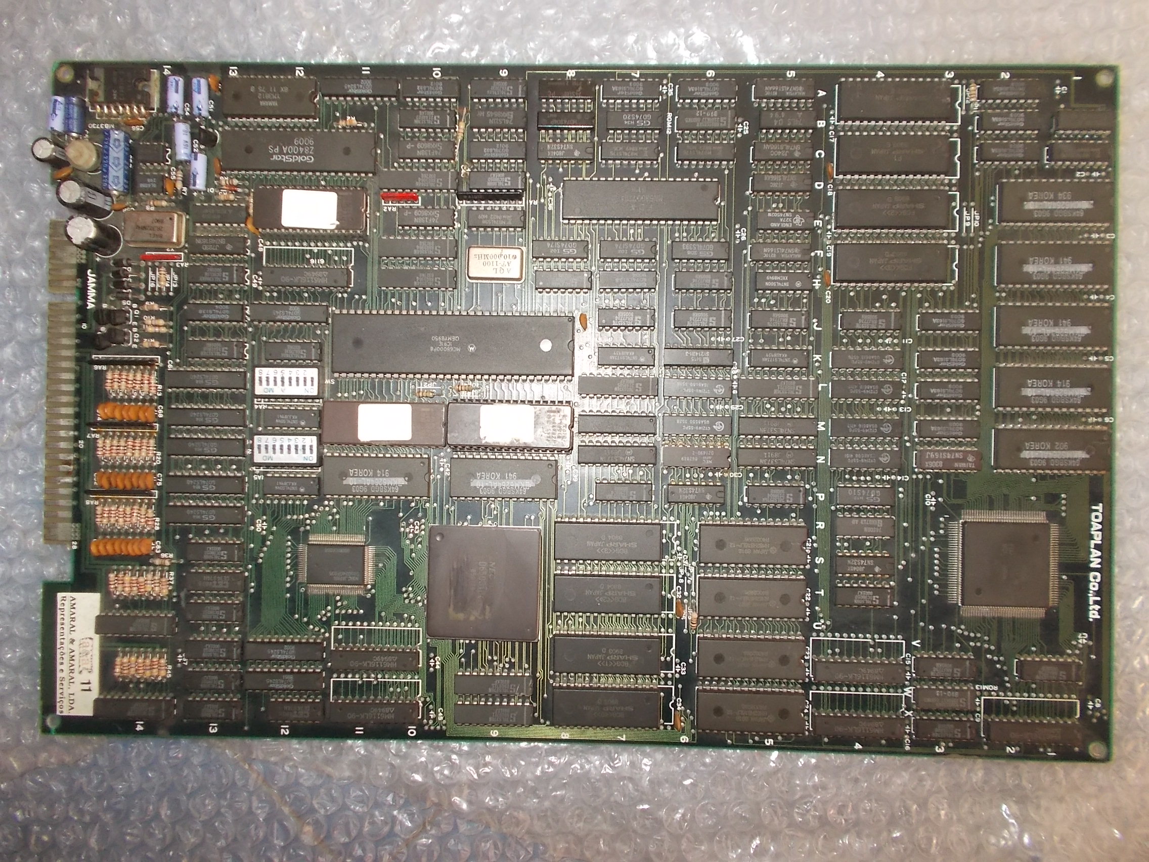
Another shoot’em up ‘under surgery’.Here we have an Hellfire PCB I received from Portugal:

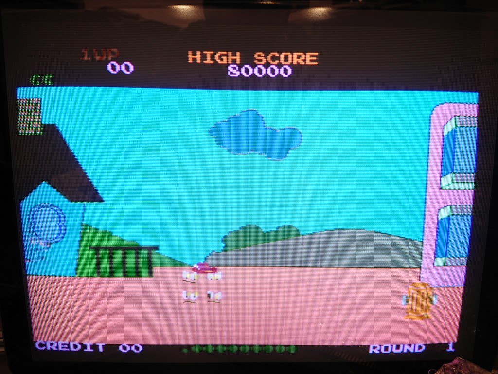
Board booted into game but sprites were all blocky:

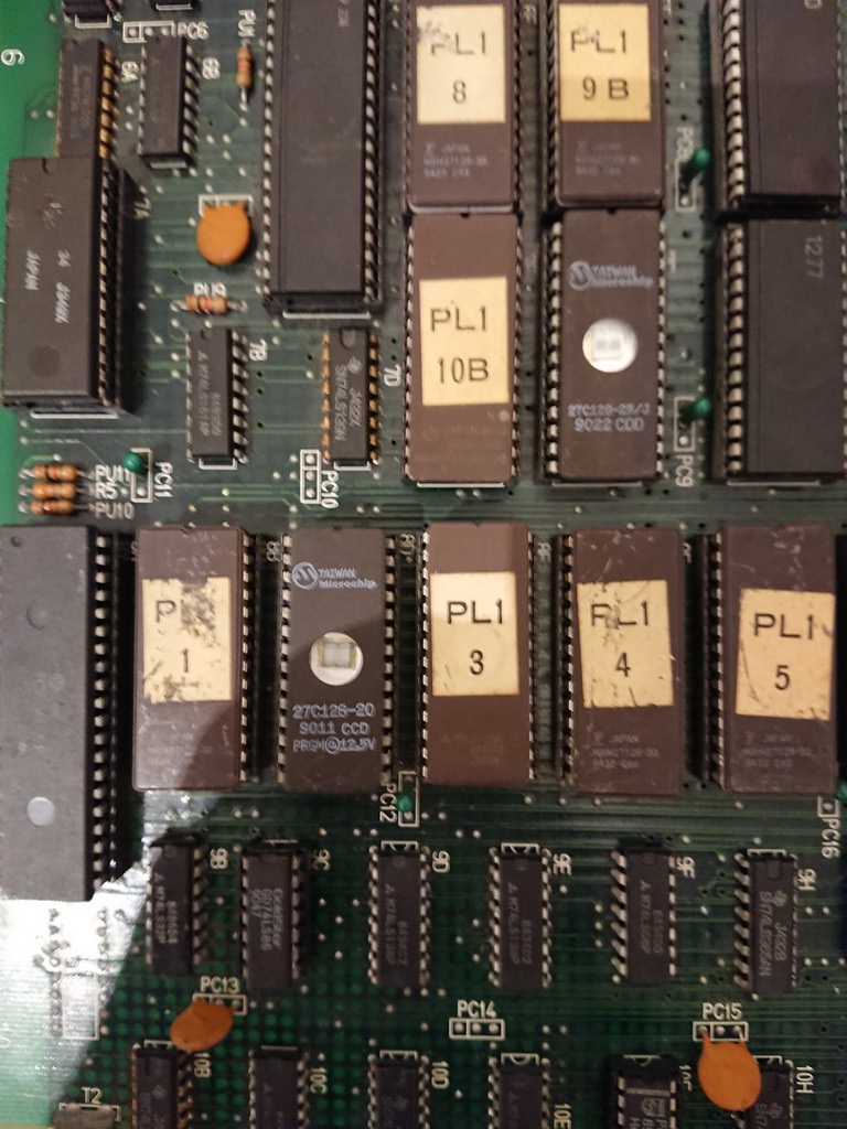
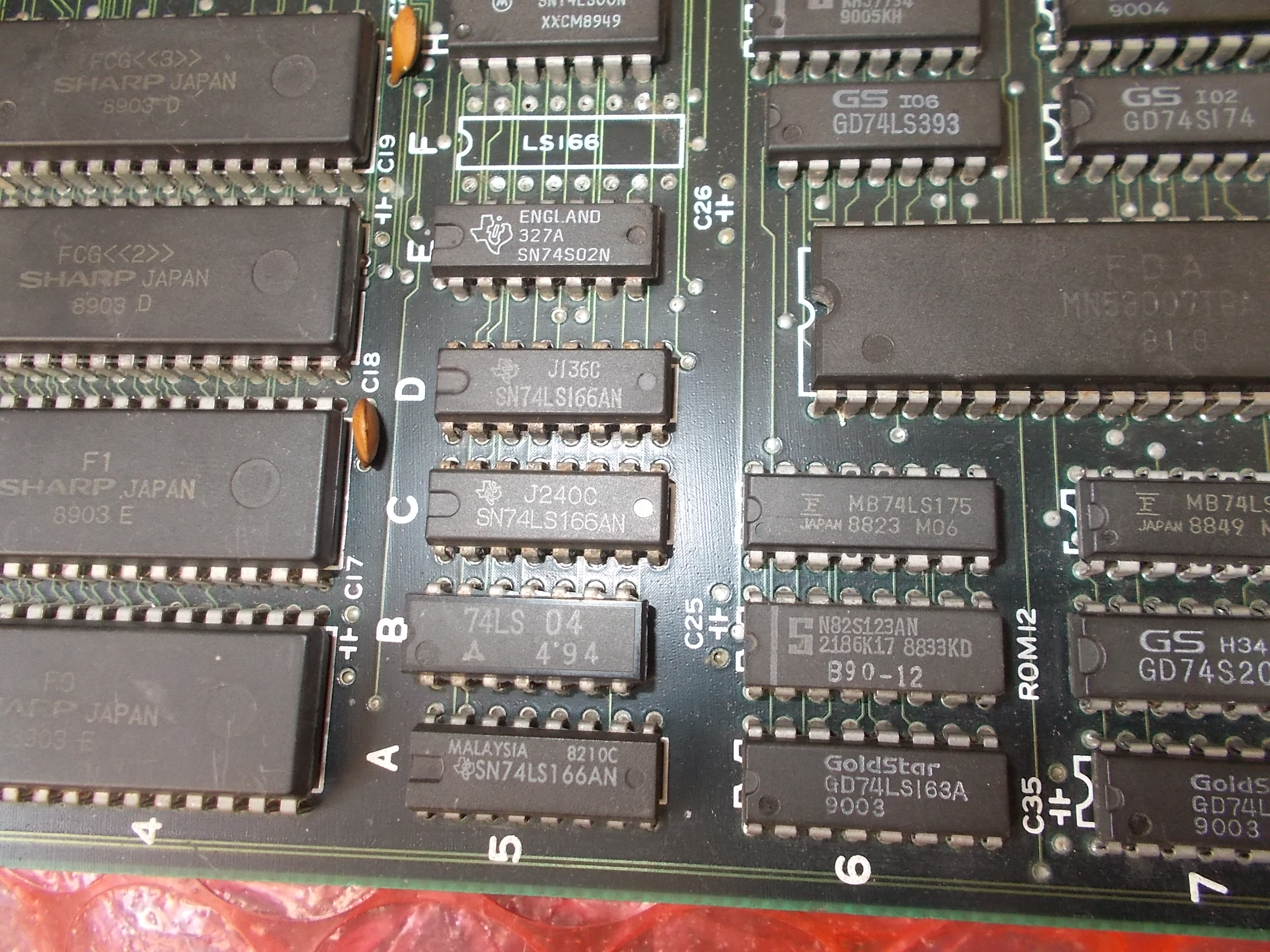
Looking at hardware I could figured out the the parallel data from the four 1Mbit MASK ROMs of sprites are converted into serial by four 74LS166 8-BIT shift registers (one for each ROM)

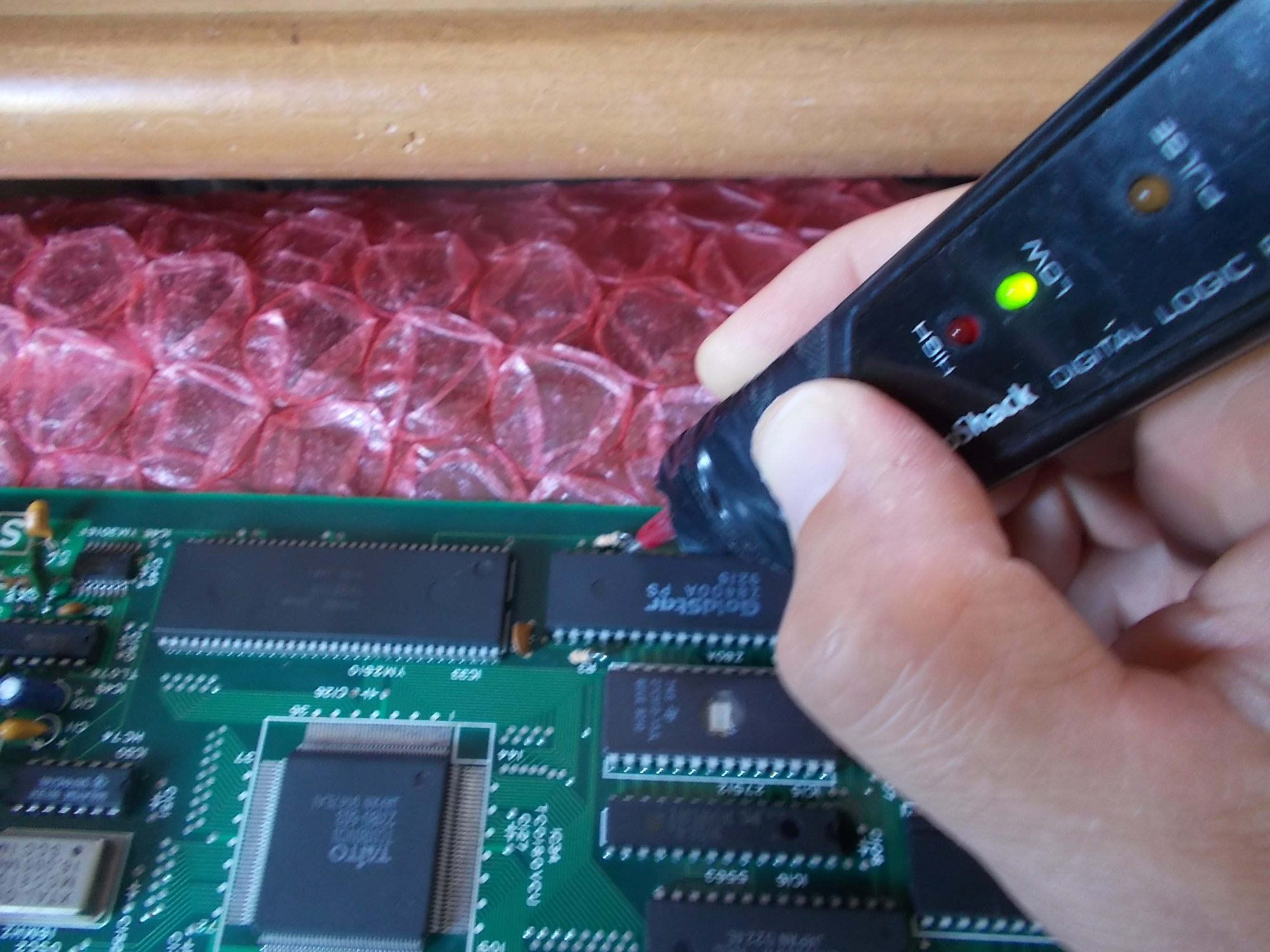
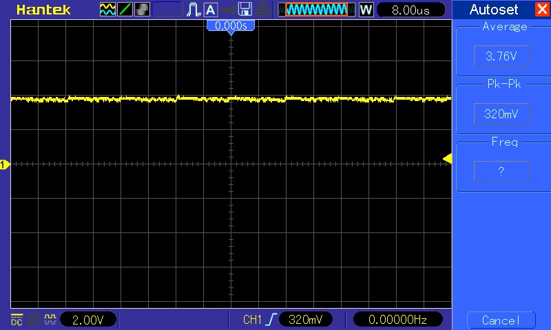
Probing the 74LS166 @5F revealed the output (pin 13) was stuck high :

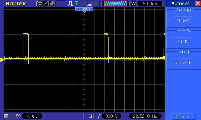
While the inputs were active:

I removed the IC:

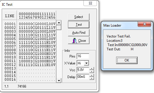
It failed the out-of-circuit testing :

This lead to an improvement  but still not perfect as sprites were missing lines :


Looking again at hardware I could figure out the sprite line buffer is made by eight 2149 SRAMs (1K x 4-bit devices, pin to pin compatible with 2114/2148)

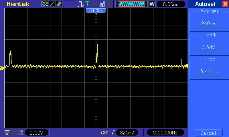
The one @6K was hot to the touch, probing it with a scope revealed weak signals on data lines :

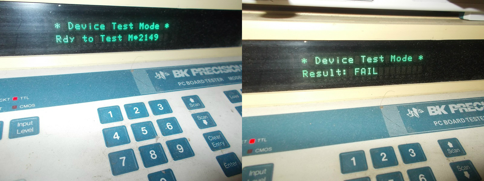
Ther RAM chip failed when tested out-of-circuit :

 This fixed sprites completely:

The last issue concerned the sound, it was faint and corrupted:

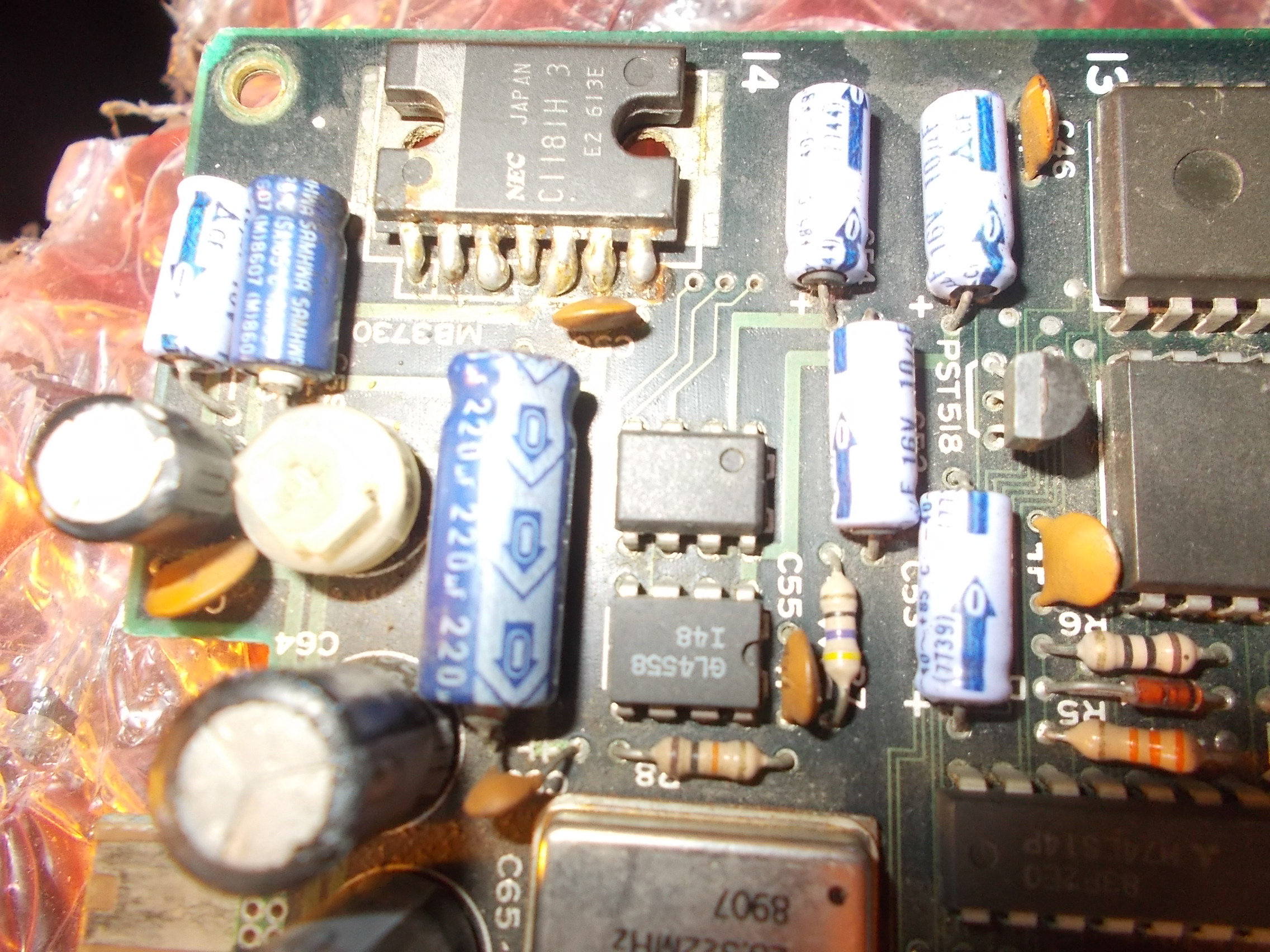
Looking at sound circuit I noticed a Nec uPC1181H amplifer was fitted in place of the Fujitsu MB3730 that silkscreening suggests :

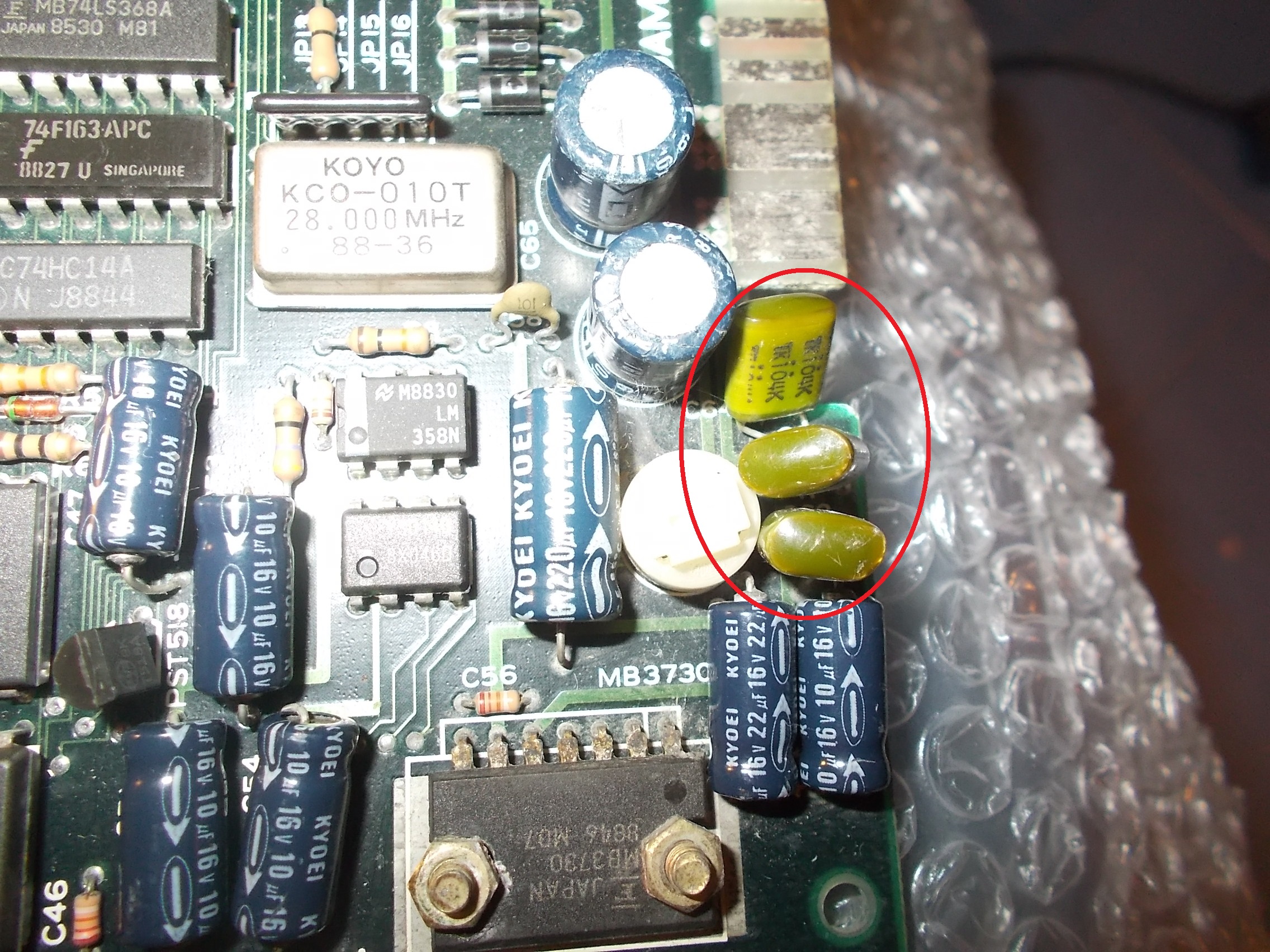
Although the two amplifiers have pretty same pinout, different is the typical application circuit and power output (14W for the MB3730 and 9.2W for the uPC1181H) so I installed a proper one.Looking at sound section on another same board I noticed three mylar 100nF capacitors were used by factory @C61-C62-C63:

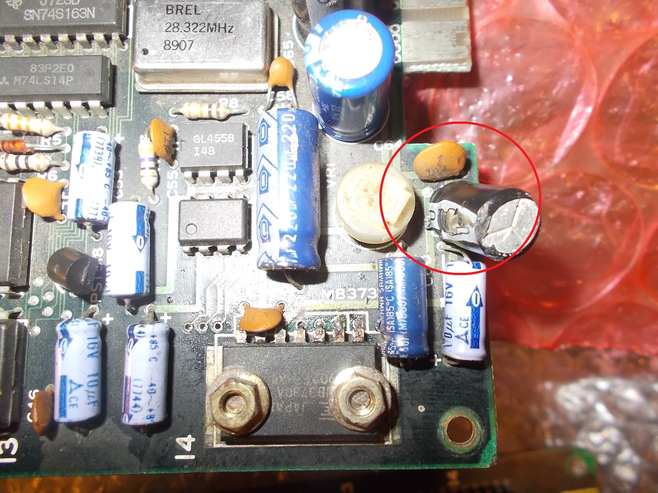
Whereas on my PCB an electrolytic capacitor was installed @C61 and the one @C62 was missing :

I restored the factory condition gaining a loud and crisp sound again.Repair accomplished.

 Posted by at 10:06 pm

Kicker (Shao-lin’s road) (bootleg) repair log

 PCB Repair Logs  Comments Off on Kicker (Shao-lin’s road) (bootleg) repair log
Oct 072018
 

Earlier this year I attended a meetup at UKVAC user Bonehead’s house.
One of the things I brought back with me was an unknown bootleg PCB that a was being given away.
I opted to take this particular PCB because it was 6809 based and I needed something to help me continue work on my Fluke 90 PC software that I started quite some time ago.

This PCB uses the Konami Classic pinout for which I already have an adapter for so following a quick visual check I plugged this in and powered up.

As you can see we have watchdogging going on.
Right next to the 6809 there are two 74LS244 buffer IC’s. A quick continuity check showed that these were connected to the address pins of the 6809.

Probing the 244 at E8 showed that all the outputs were dead. Removing this revealed a broken trace.

At some point in its life there has been a sort here.
I patched the break and fitted a socket and new 244 buffer and checked for shorts before retesting.

Powered up and all was well again.

Confirmed later that the sound is present too and controls are all working.
A quick fix this time.

 Posted by at 5:55 pm
Oct 052018
 

Another PCB which has been collecting dust on a pile. I got myself motivated to repair it.

Symptoms

The PCB will not boot, all you see is a white screen.

Decided to check the clock circuit first to ensure the CPU was running, it was, so clock circuit is fine. Next I checked the CPU ROMs, and found a bad ROM at location 8N. Burned a new ROM and inserted it, now game is booting but with issues.

There were absolutely no sprites, and I could not coin the PCB up to start either. The background was full of jail bars.

I first checked the sprite PROM on the A board at 2E, if this goes bad the sprites will dissapear. Both the PROM and socket checked out good. So, my attention turned to the lower B board as this handles all the sprite processing.

It is interesting to note that GnG PCB will boot without the B board but without sprites of course. Handy for troubleshooting.

These Capcom PCBs have all the copper path traces masked, obviously an attempt to stop the bootleggers. Luckily, schemes are available, and they are sectioned off into relevant areas of the PCB which is nice.

My attention turned to the B board to get the sprites back up. Found a LS139 Decoder IC on the B board at 9K which for some reason was plagued with rust, I checked it and found that it was completely dead, the rust must have worked its way up.

Socketed and replaced it and now we have some sprites which are all wrong, but at least we have sprites.

Looked around the graphics ROM addressing circuit and eventually found a LS194 Decoder on board B at location 4C with pins 13 and 14 stuck high.

Socketed and replaced and now the jailbars have gone.

Whilst I was troubleshooting, I noticed that the RED had completely failed and I was left with just BLUE and GREEN, nice! I checked the supergun setup, but no it was the PCB which had failed.

I carried on looking at the sprite circuits and found a LS273 Octal Flip-Flop which had completely failed.

Socketed and replaced it, we now have all the sprites back!

I flipped the PCB over to look at the A board, and using the schemes I could see that a LS367 Hex Bus at location 6C was the final stage for the RED output. I checked it and found that pin 11 was stuck High.

Socketed and replaced it and the RED came back!

Finally, had to resolve the issue of the PCB not coining up. The coin up function works in the same was as the game inputs, so I knew I was looking for another LS367 Hex Bus on the A board. I checked the schemes again and it told me the LS367 Hex Bus at location 8A controlled the coin up input. I checked the LS367 and found pin 4 was stuck Low.

Socketed and replaced it, now coining up.

PCB finally repaired.

Galaga ’88 repair log

 PCB Repair Logs  Comments Off on Galaga ’88 repair log
Oct 052018
 

I’ve had this PCB on a pile for nearly two years, decided it was time to look at it.

Symptoms

There is no Green on the graphics, Red and Blue are fine, but colours look washed out because of this.

Started at the edge connector, and using the probe checked the Green pin and it was stuck low, the Red and Blue were pulsing nicely as I would expect.

Traced the Green video path all the way to the second layer which is the main CPU board and smaller. Found a Transistor (TRM3) which had been crushed and legs were shorting, effectively grounding the Green video.

Straightened it out and all good now, full colour is back.

Thing to note is that these Transistor protrude quite a bit, and since these Namco System 1 boards do not have legs, the board tends to sit resting on these Transistors. One to watch out for if you lose a colour on a Namco System 1 board.

Ikari Warriors repair log #2

 PCB Repair Logs  Comments Off on Ikari Warriors repair log #2
Oct 052018
 

Symptoms

The PL1 Ikari character keeps going up on its own when I start a game, the PL2 Ikari is fine.

Looked at my rotary stick, could not see any problems, so I disconnected the sticks from the PCB. The PL1 Ikari character was still going up on its own.

Next I looked at the SNK to JAMMA adaptor, saw no problems here, the fault must be on the PCB.

The PCB is an original SNK three layer PCB set, and uses SNK pinout.

I determined which pin on the edge connector was used for PL1 UP, and traced it back to a SIL resistor array, followed it through a 0.1uf ceramic capacitor where it went to a Hex Buffer 74LS367 at location D4 on the top layer of the PCB stack which handles the joystick inputs.
Bought out the logic probe, and found that Pin 2 (output) on the Hex Buffer was dead. Desoldered it and put the Hex Buffer into my IC Tester which confirmed that Pin 2 had failed test.

Offending Hex Buffer, a Fujitsu branded variant;

Soldered in a new 74LS367 Hex Buffer, all working great now, PL1 Ikari no longer has suicidal tendencies.