While searching through some documents from Data I/O I came across a bunch of logic diagrams for various PLD’s. One of them was for the CK2605.
As I’ve not seen this in the wild before I thought I’d upload it.
*click the picture for PDF
Some time back I bruteforced the A-17480 PAL16L8 chip from Mortal Kombat II. This was untested until recently when UKVAC member JonHughes tested it and found it didn’t work properly.
We tried several things but always got the same issues so he sent me his full PCB to do some testing of my own.
While I could find anything wrong from an operation point of view I did find that the original TIBPAL16L8-10 PAL chip transitioned states about 4ns faster than the fastest GAL chip I have to hand. I had experimented with GAL’s ranging from 10 to 25ns but the slower ones did just make the issue worse.
In desperation I ordered a NOS TIBPAL16L8-10 from eBay (not too cheap these days) in order to be 100% sure of my work. The result was a perfectly running game.
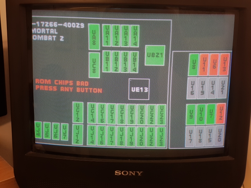
So what are the issues? Well not a lot really. A GAL substitute will still allow the game to play very well but it did show errors during the POST
The game itself also plays fine but there are some graphical issues here and there, most noticeably on the ground during actual gameplay.
On the video you can see the ground keeps glitching black. This is pretty much the only fault I can see but its definitely worth noting
The video is not the best quality, capturing CRT screens with my phone is never great but hopefully you can see.
Due to certain things that have been going on elsewhere on the internet I have made the decision to remove the SEGA ROM’s from this site.
I have not personally been asked to take these down but given what I’ve seen happen recently involving SEGA ROM’s and previously with Nintendo too I thought I would play it safe and remove these files.
Sorry for any inconvenience
The PLD Archive is currently in the process of being moved to a new wiki.
There may be a delay is adding new files while the wiki get populated. This is currently over half way done but the process is long and tedious bear with us.
In addition to the normal PLD files there is also scope to add more detail and pictures so if anyone has any good quality PCB pictures or extra information like missing PLD IC location details or names then please let us know.
The old table will be kept up for now until we are sure all the detail has been moved over correctly.
You can take a look at the wiki at
https://www.jammarcade.net/wiki
Although I grew up with a Commodore 64, I have a soft spot for Atari 8 bit machines. My mission in life is to save them all from going into landfill.
I spotted this grimy Atari 800XL on Gumtree very recently as untested, it came with an Atariwriter Word Processor Cartridge. I met the friendly chap selling the item and we did the exchange for the computer at Town Hall steps, which is a popular meeting place in Sydney.
Taking the machine apart, I was happy to see that the machine was fully socketed and that the PCB was in excellent condition despite it needing a good clean. Actually, I was expecting a fully socketed machine because it was made in Hong Kong just like my 600xl was. Another pleasant surprise was the brand of DRAMs used ( OKI ) instead of the mT variety, which have a bad reputation for reliability and were used extensively in the Atari 8 bit and C64 line.
I had a close friend of mine over after work and we went through the troubleshooting together. Unfortunately, not much happens after power it up. A black screen most of the time and sometimes an intermittent picture, obviously this is a sync issue.
Sometimes I manage to get a screen that looks like this. This is a good sign. At least I know the CPU, ROMs and DRAMs are working to some extent to produce this screen.
Luckily I have a fully socketed 65XE to swap parts to and from. I also tried a known semi good GTIA which was bad on one output only but produced a nice clean picture in a working machine. The GTIA is responsible for generating the luminance, color and csync signals to produce an image to the screen.
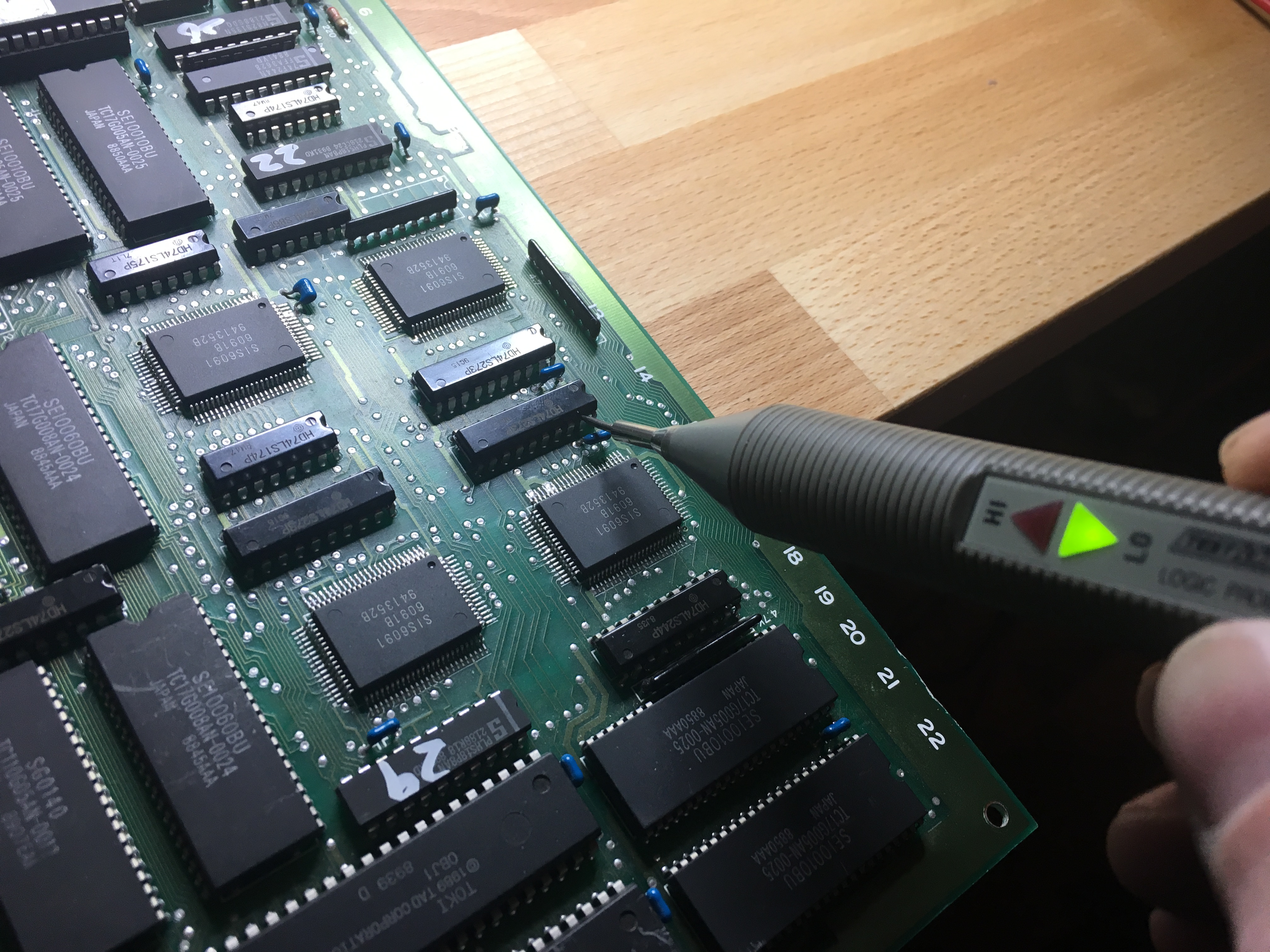
Replacing it doesn’t change a single thing so I consult the schematics, the signals go directly to a hex non inverting buffer ( 4050 ) so I switch my logic probe to the CMOS setting and start probing the chip. Output 6 ( lum0 ) is good, lum1, 2 and 3 were all bad and all outputs were floating. I wanted to check the CYSNC line ( composite sync ) and that was also floating ( no signal at all ).
I short the input and output pins of the 4050 ( pins 14 & 15 ) with my logic probe briefly which restores the picture to the screen.
Replacing the chip completes the job!
Now onto the next challenge, cleaning the motherboard and case!