Porchy

Pac-Man repair log #2

 PCB Repair Logs, Repair Logs  Comments Off on Pac-Man repair log #2
Feb 142016
 

I recently asked on UKVAC if anyone had a Pac-Man PCB I could borrow in order to test the recreations of the two custom chips I made for the CPLD replacement device.
JonHughes replied and a few days later I had not one but two PCB’s to play around with.
One was pretty much stripped of parts but the other was complete and even had the TTL versions of the two customs.
I already have a JAMMA adapter for this that I made for my first Pac-Man repair so I was all ready to go.
Visual inspection revealed nothing to be concerned about so I went ahead and fired the game up.
I got nothing. The game was absolutely dead. I checked for activity on the CPU address and data bus but they were static.
Checking the clock pin also showed up no activity. Probing around the clock section suggested that the crystal had died so I went ahead and replaced it but this didn’t help.
There was a small build up of old flux around capacitor C4 so I went ahead and cleaned this up. The clock signal came back!

So now I had this my clock back and activity on the address and data bus lines but I still had a blank screen and it wasn’t making any noise. I also confirmed the board was not watchdogging.
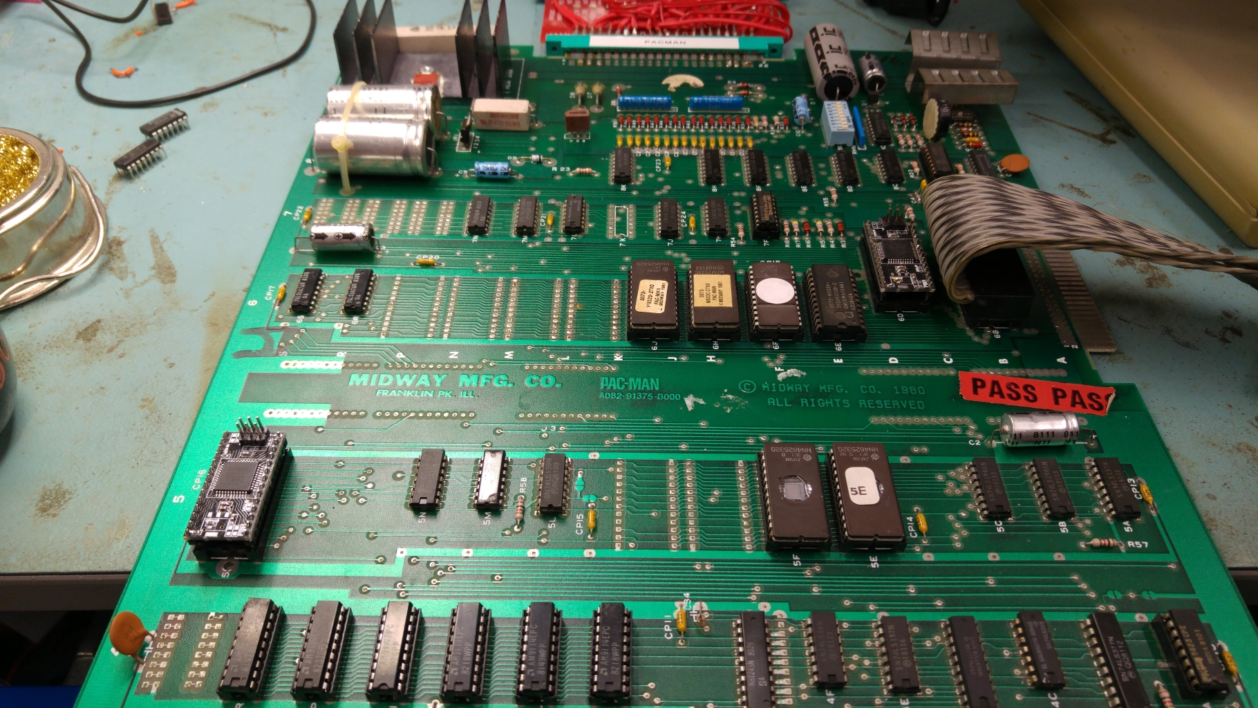
Since the Z80 CPU is already socketed I decided to use the Fluke 9010 to check the ROMs/RAMs. Here is where a little problem came as the TTL custom replacement covers over the Z80 so I fitted a few header to the pins to raise it up enough to fit the Fluke pod.
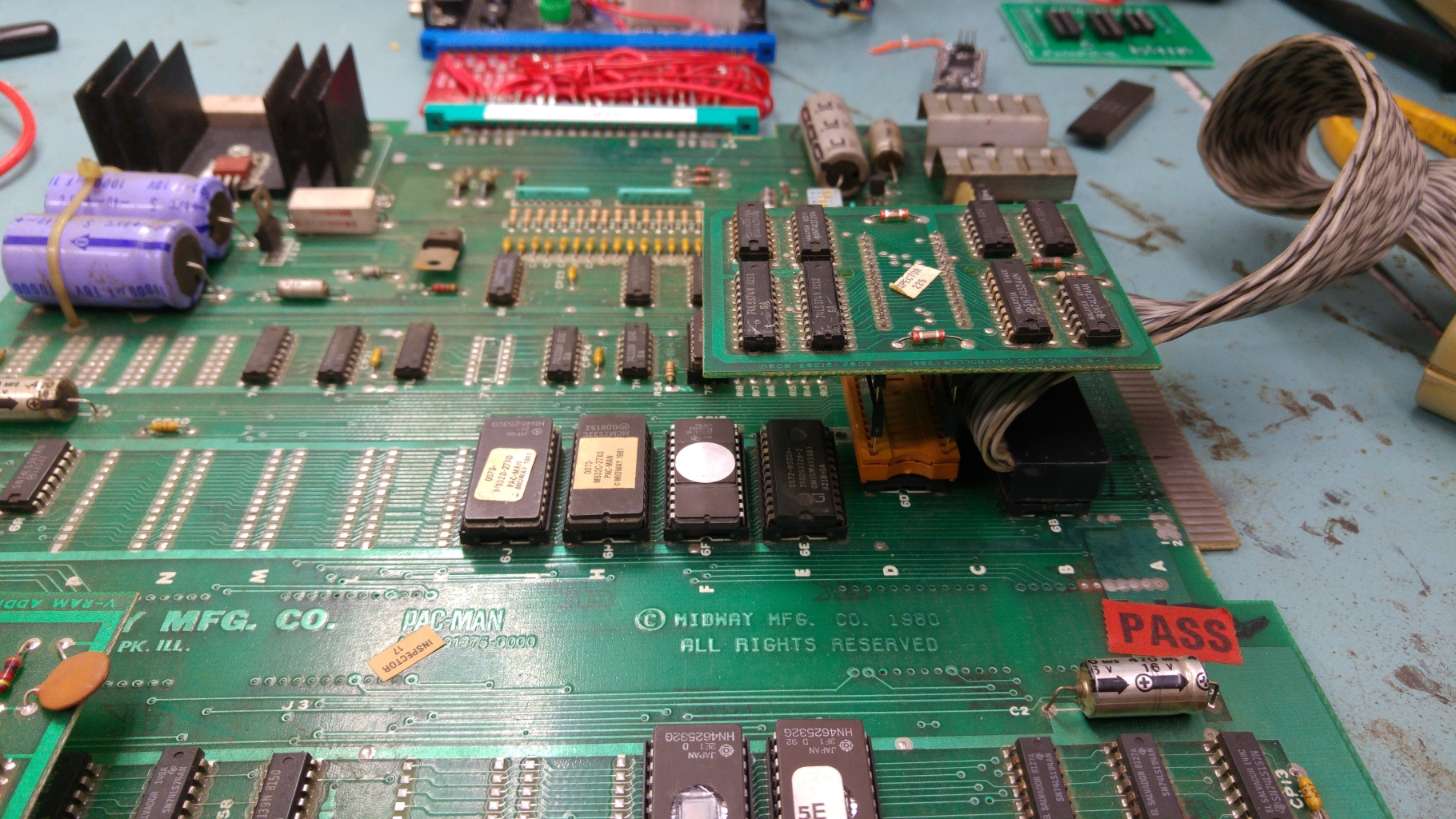
20160206_195844
With the Fluke connected I quickly verified the ROM’s and RAM’s were fine. It also verified that the connections between these chips and the Z80 were good.

Next step was to work backwards from the RGBS pins at the edge connector.
There was obviously no video output.
I found there was no activity coming out of the 74LS157 at 3A but some activity going in and to/from the connecting chips.
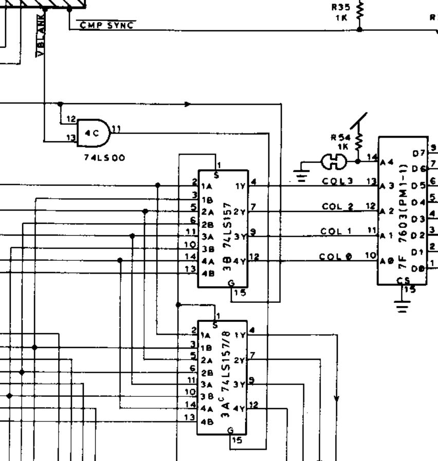
pacman_strobe

Checking the strobe pin (pin 15) of this chip I found the signal was stuck HIGH which basically means the chip was disabled.
Checking the 74LS00 at 4C showed I had activity on pin 12 but pin 13 was stuck HIGH. This being the /VBLANK it was clear that this was not correct.

The /VBLANK signal is given out by a 74LS74 chip at 5M.
Checking the signals on this chip I found the clock signal was stuck LOW.
pacman_vblank

This clock signal is 16V signal that is generated by a couple of 74LS161 4 bit binary counters.
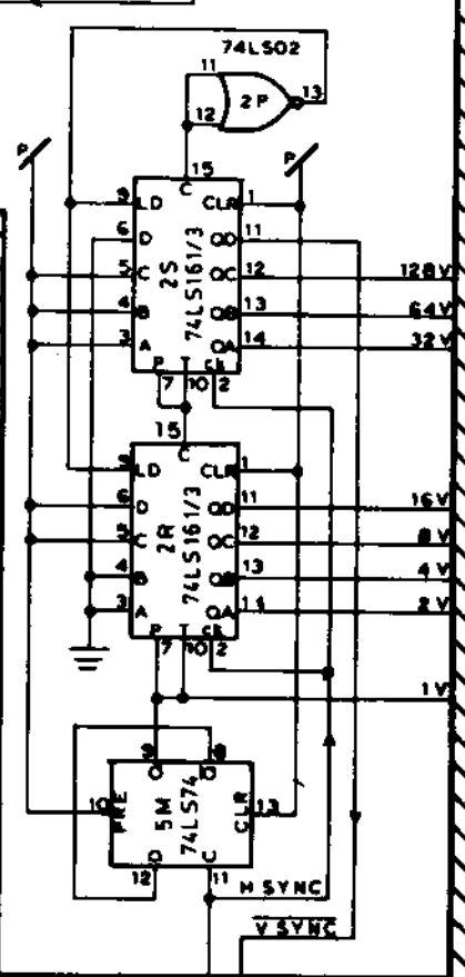
pacman_counter

According to my logic probes there was no activity on pins 11 and 12 of the 74LS161 at 2R (the one that generates the 16V and 8V signals) but seeing as though this chip was already in a socket and it tested good in my chip tester I didnt believe what the probe was telling me so I fired up the scope to take a look at those pins.
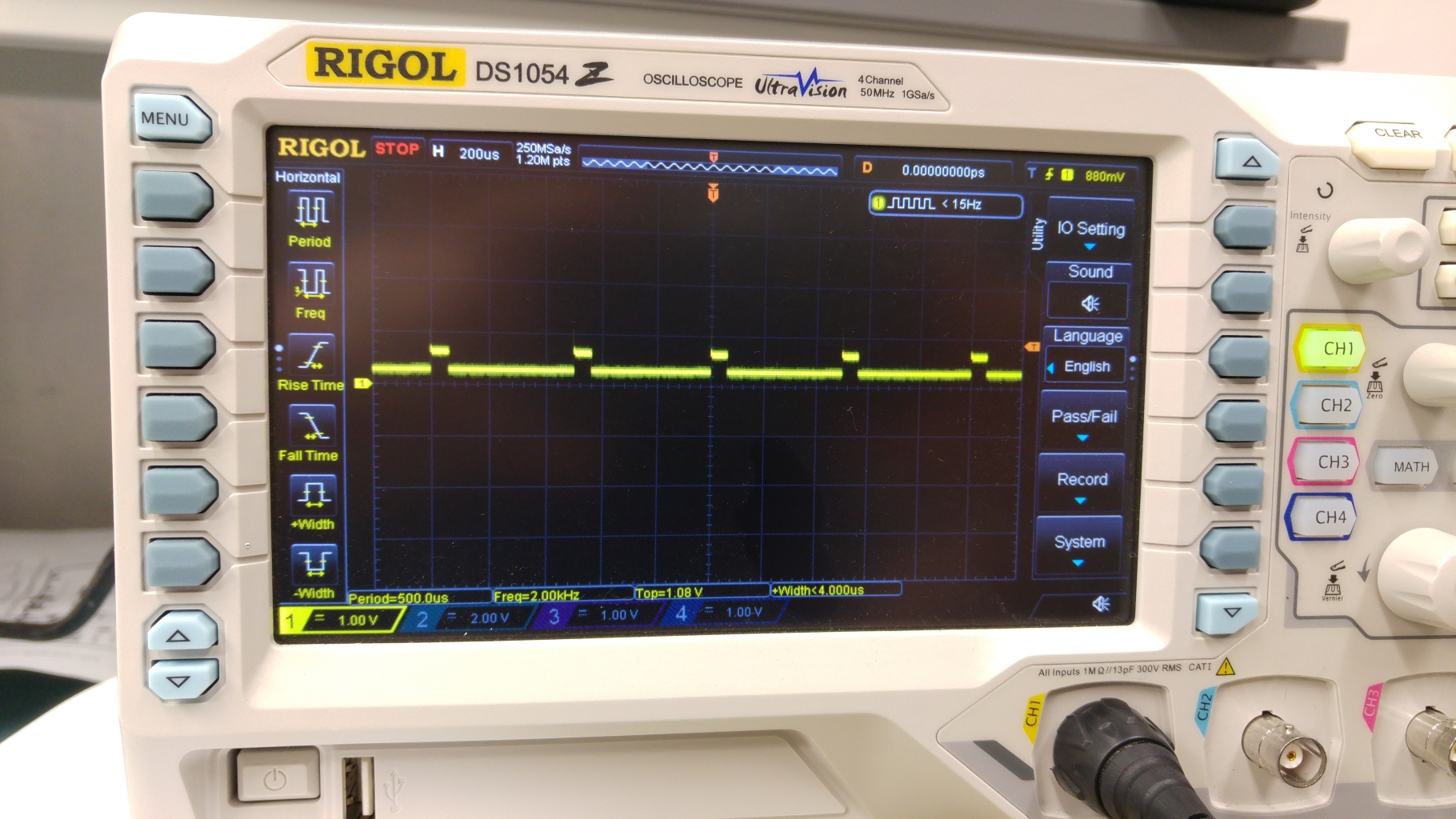
20160214_165521

This is a good clear example of signal contention. You can see that the signal is trying to rise up but only getting to about half a volt. Knowing that the chip is actually good out of circuit confirms that there is another signal driving it low.
I found that pins 11 and 12 were shorted together.
I couldn’t see anything really wrong physically on the board where these two signals went so once again I opted to clean off the small bit of old flux I could see and once again this fixed my problem.
Although I’ve read about old flux causing issues I’ve never actually seen it myself until now so this has been a lesson learned for me.

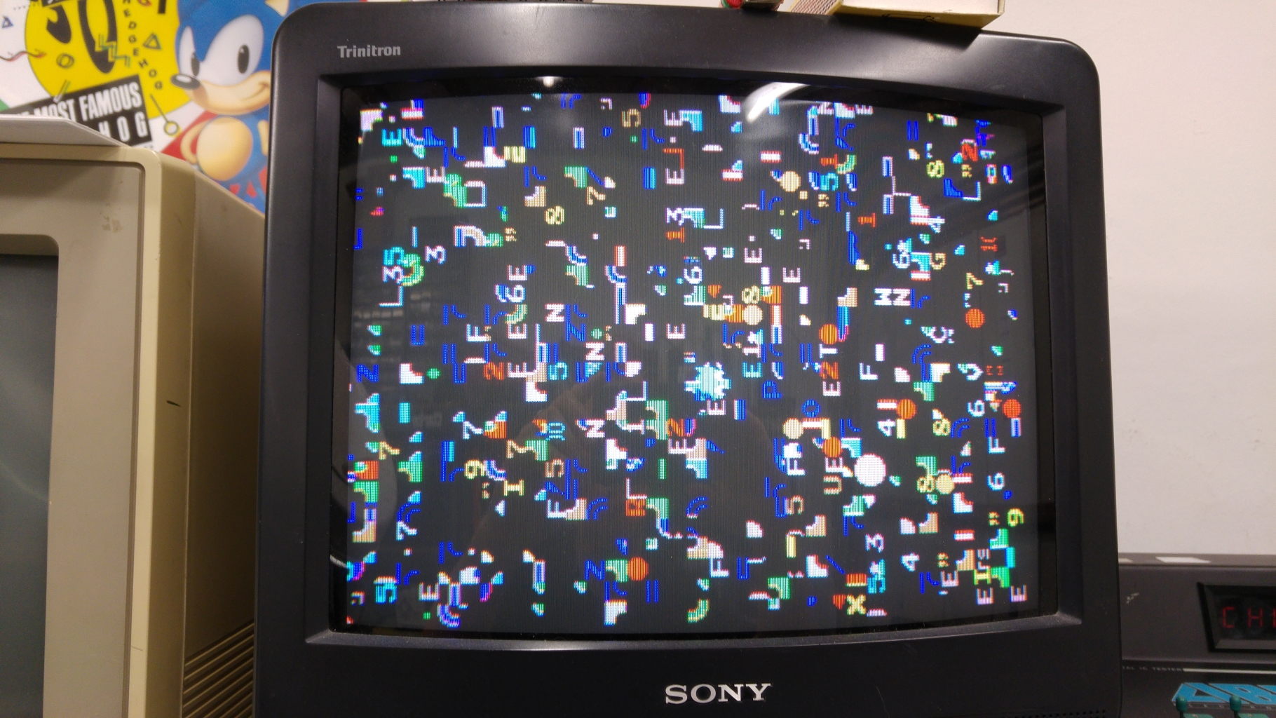
Now I got this.
20160214_171848

The game is actually running here but there is garbage on the screen. If I left it running all the sprites came on the screen and were complete.
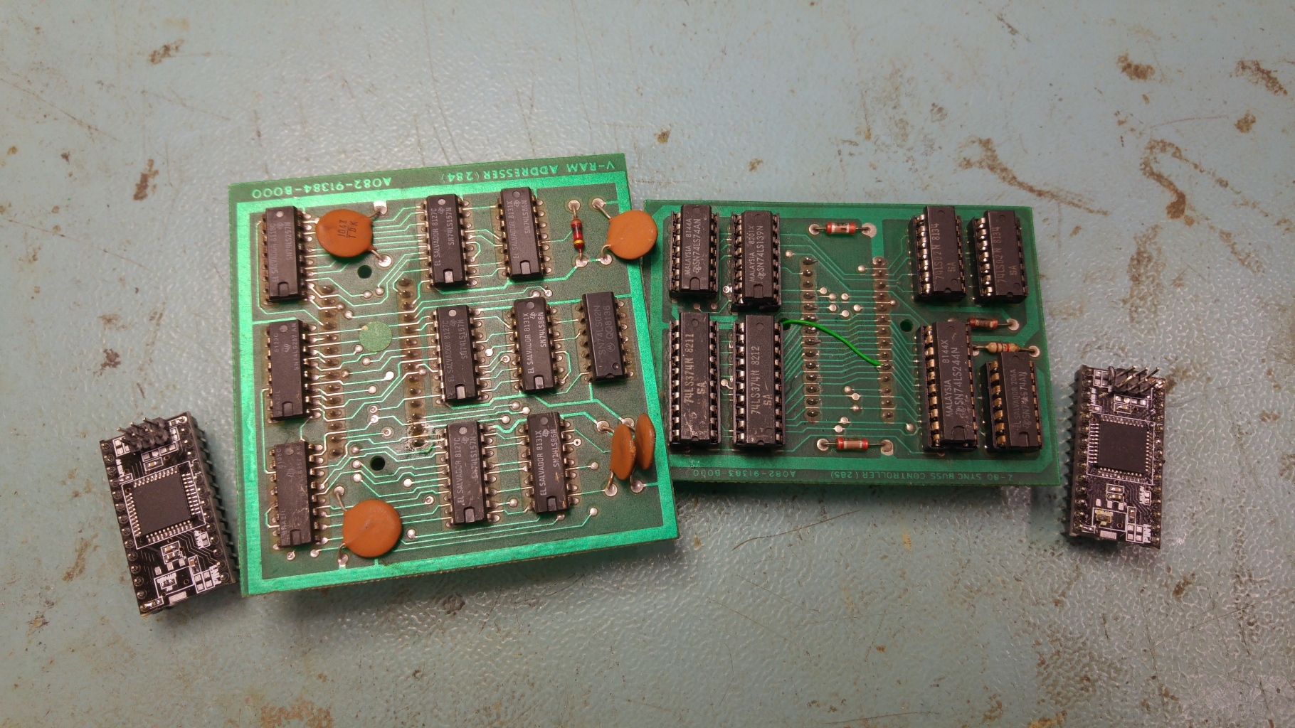
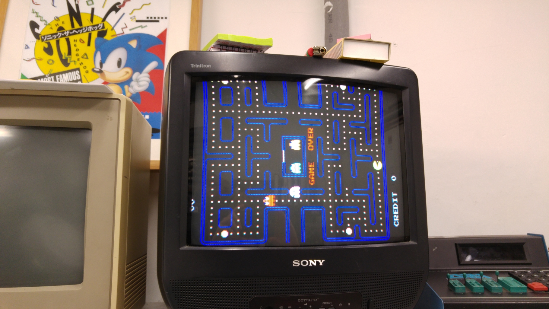
Before moving on I decided to test out my CPLD implementation of the syncbus controller custom. This gave me the same output so was confident it was OK. Now I though I’d try out the VRAM addresser replacement too and I got this.
20160214_183515
20160214_183521

All fully working with sound too.
The actual cause of the earlier fault was created by me as I had bent 2 pins on the VRAM module during one of the many remove/replace cycles I had done. I since confirmed this works fine too.

That’s this board fully working and the two replacements confirmed working too.

Thanks to JonHughes for providing me with these boards.

 Posted by at 8:36 pm

Pacman Sync bus controller and VRAM addresser

 General  Comments Off on Pacman Sync bus controller and VRAM addresser
Feb 142016
 

Today I have been able to test my recreations of the syncbus controller and VRAM addresser in ColinD’s 28 pin replacement.
Both files can now be downloaded.

20160216_202152

 Posted by at 7:38 pm
Feb 062016
 

I’ve been doing a lot more gaming than anything else recently so thought I’d do a little post on this.
My hardware of choice right now is the Atari Lynx. The only thing that lets the Lynx down for me was the screen. Anyway A guy known as McWill found on the AtariAge forums makes an LCD replacement so I took the plunge and ordered one.

Installation was a little time consuming but definitely not difficult. I found the hardest part was dealing with the Lynx unit itself, it gets a little awkward reattaching the flex cable.
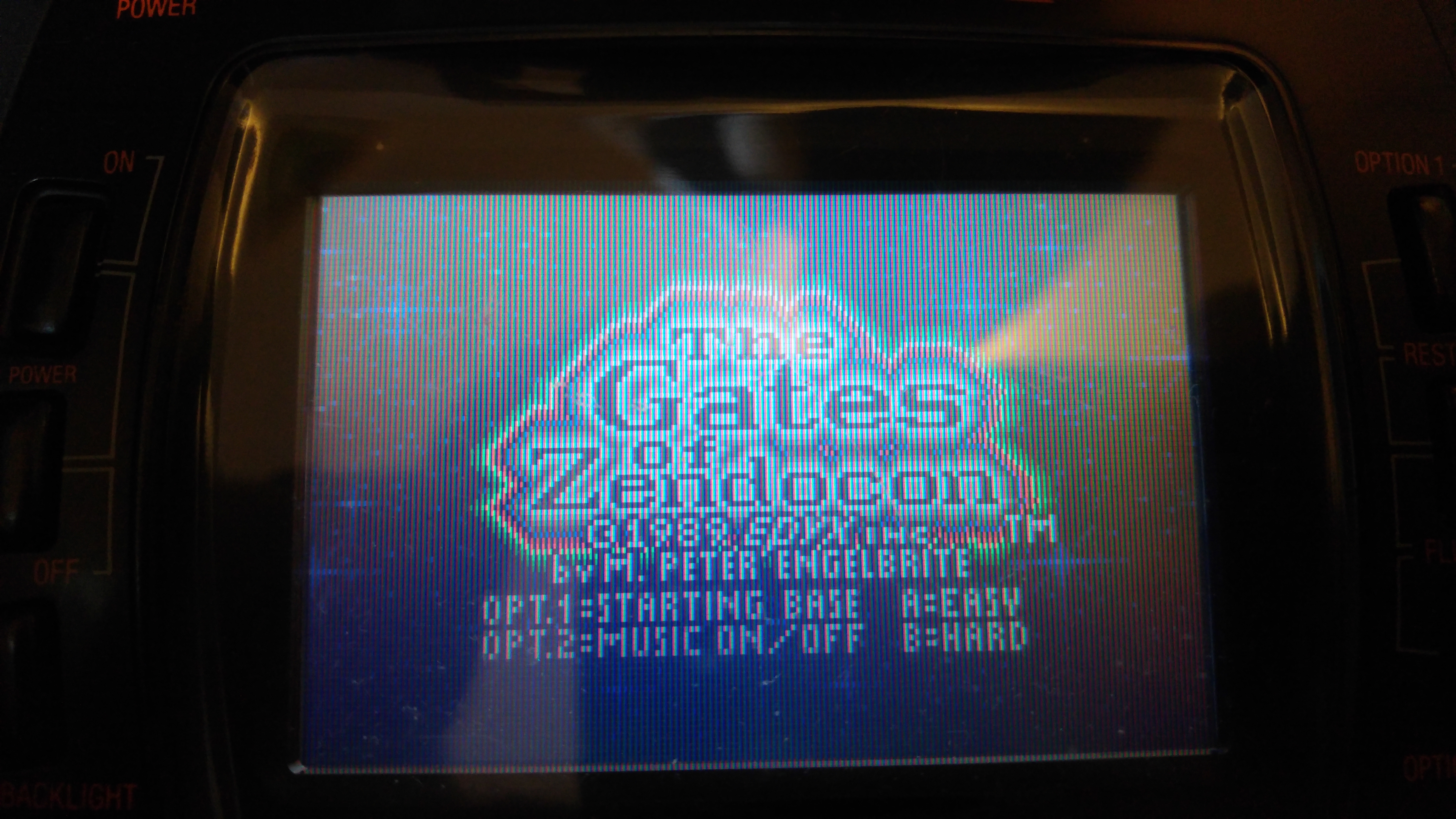
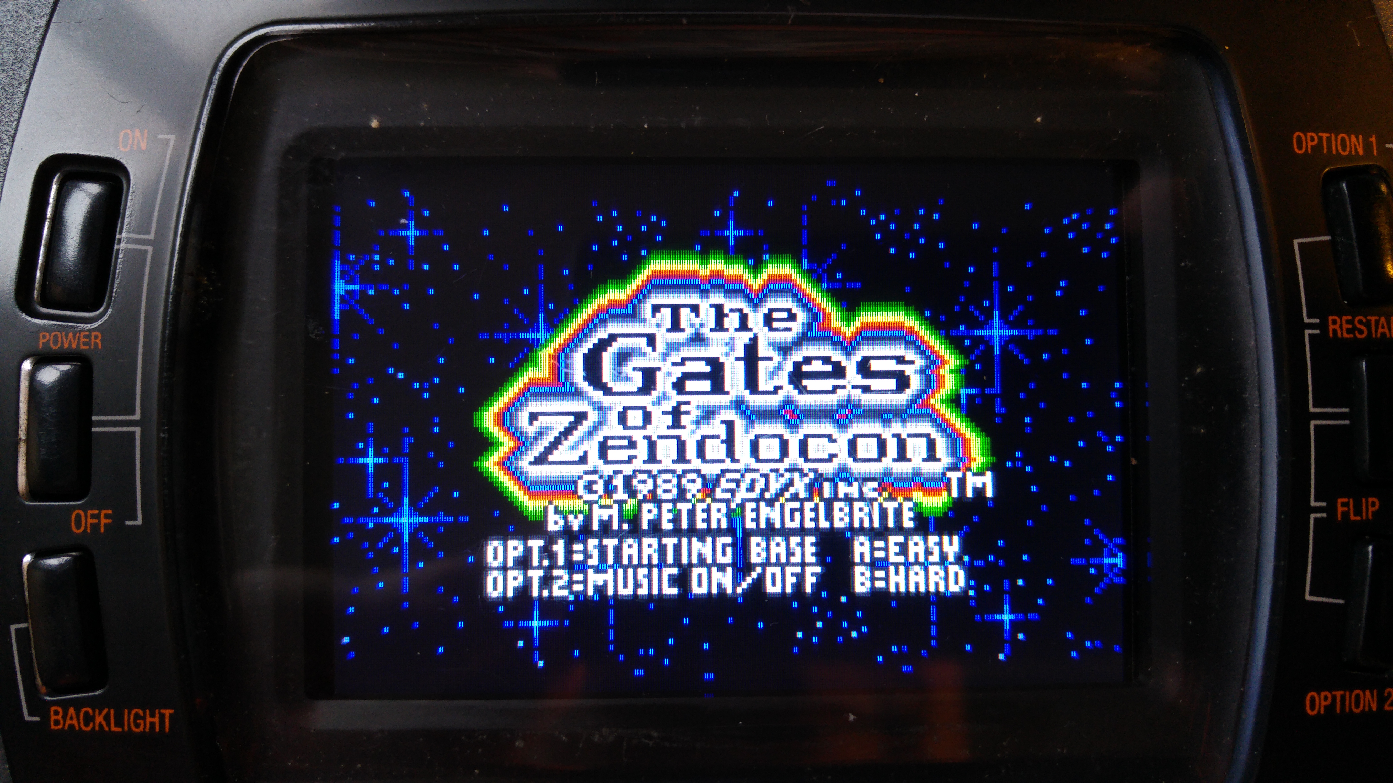
For some reason I never took a picture of the replacement itself so ill just show the before and after screenshots.

BEFORE:
20160206_100625
AFTER:
20160206_121525

Im very impressed with this thing. Pressing the backlight button will switch on/off scan lines too which is a nice touch.
Ill definately be getting a lot more use out of my Lynx now.

Thanks to McWill for this. Delivery took just a few days (from Germany to UK) and was very well packed.
Game Gear is next on my list when funds permit.

 Posted by at 1:36 pm
Jan 242016
 

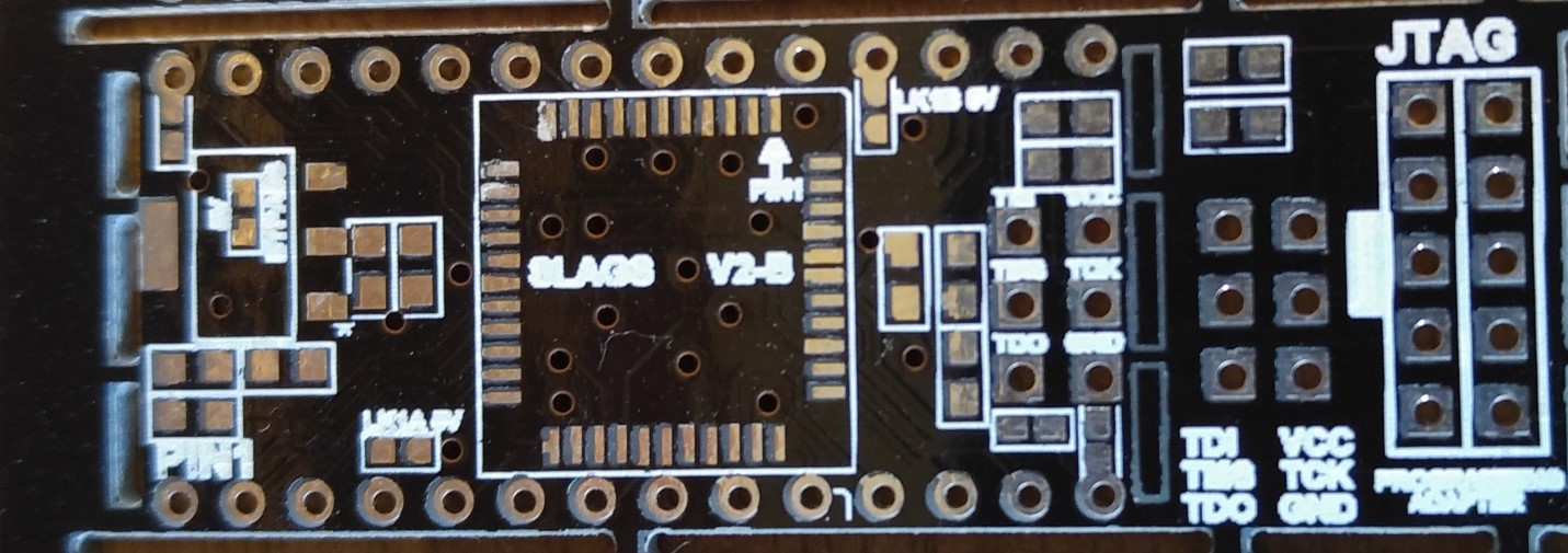
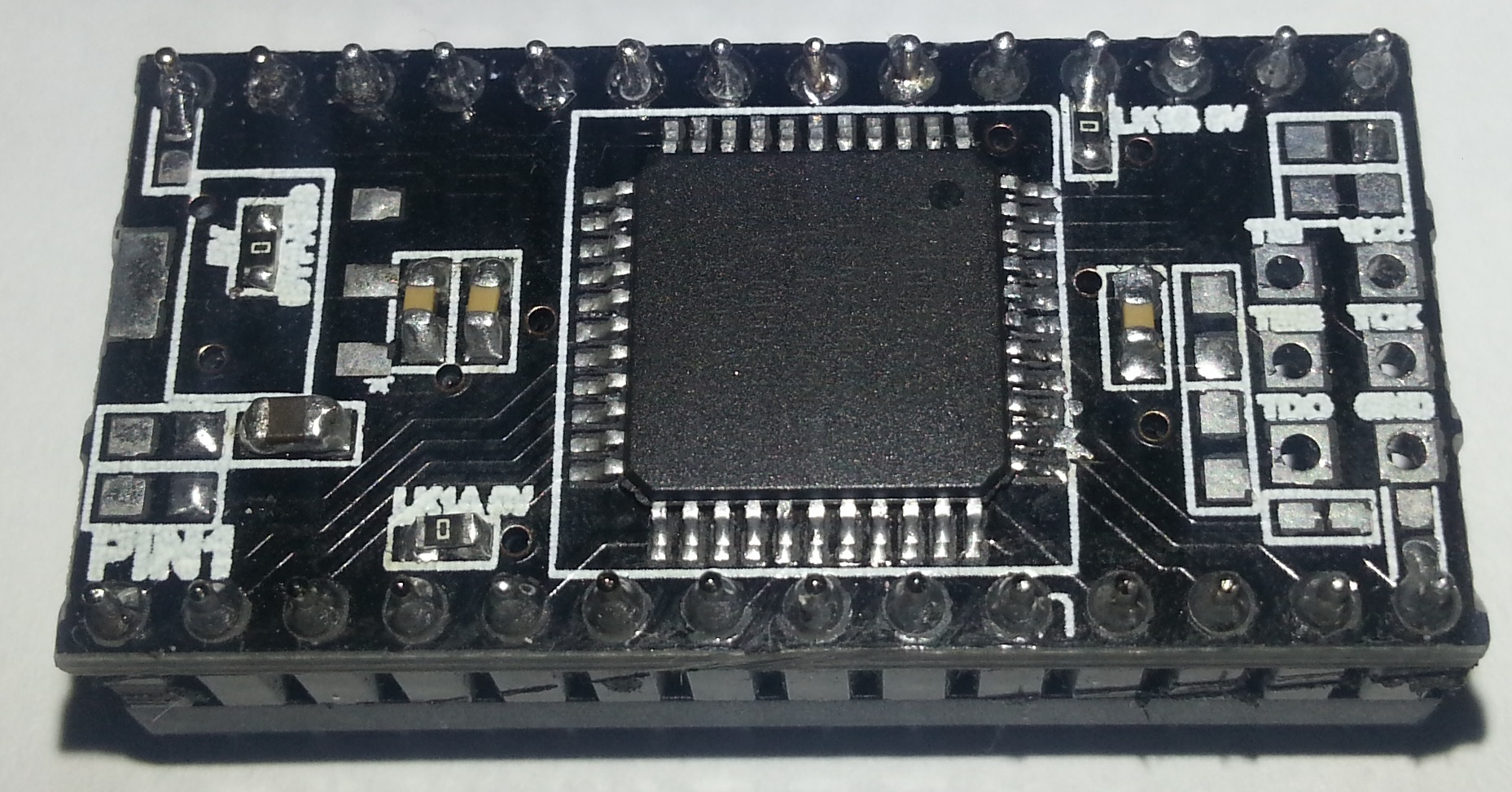
Some years ago MikeJ from FPGAARCADE made a 28 pin CPLD replacement that could program to replace certain custom chips from a variety of arcade games and even the Commodore 64 PLA.
While I was waiting for Mike to get another batch of his boards ready, ColinD on the UKVAC forums contacted me telling me about his own project.
The concept is essentially the same as Mikes but his was originally geared towards replacing the SLAG chip on some Atari games. It does however have multiple links available so it can be configured into what we call ‘normal’ mode. This makes it so the power pins are in the corners like with ‘normal’ chips/EPROMS/etc. It also has space for a 3.3v regulator so a XILINX XCR3064XL CPLD can be used in place of the EPM7064 that I’m using.

20160123_115449-1

big_slags

My first project for this was to reverse the Konami 501 custom chip. Luckily I have a one of the bootleg versions of Time Pilot here courtesy of Muddymusic that has the same layout as the original board but all the customs are implemented in TTL on riser boards so reversing this was a matter of drawing out the schematic.
I eventually got something that let the game boot and work but there were some graphics faults here and there. This ended up being an issue with using a modern part to replace old parts. The propagation delay on the CPLD is a lot less that the original TTL part. This was solved by enabling the ‘Slow Slew Rate’ option in Quartus II.

So with the 501 reversed and the chip I have confirmed working I’ll set about doing the others on this board.
I’ve yet to test them on genuine hardware but I remain hopeful.

The original thread of Colin’s can be found here.
If anyone is wanting one of these then you can PM user ‘ColinD’ on the UKVAC forums.

 Posted by at 6:10 pm

ABI ICT-24 Digital IC Tester tech info

 Technical Info  Comments Off on ABI ICT-24 Digital IC Tester tech info
Jan 012016
 

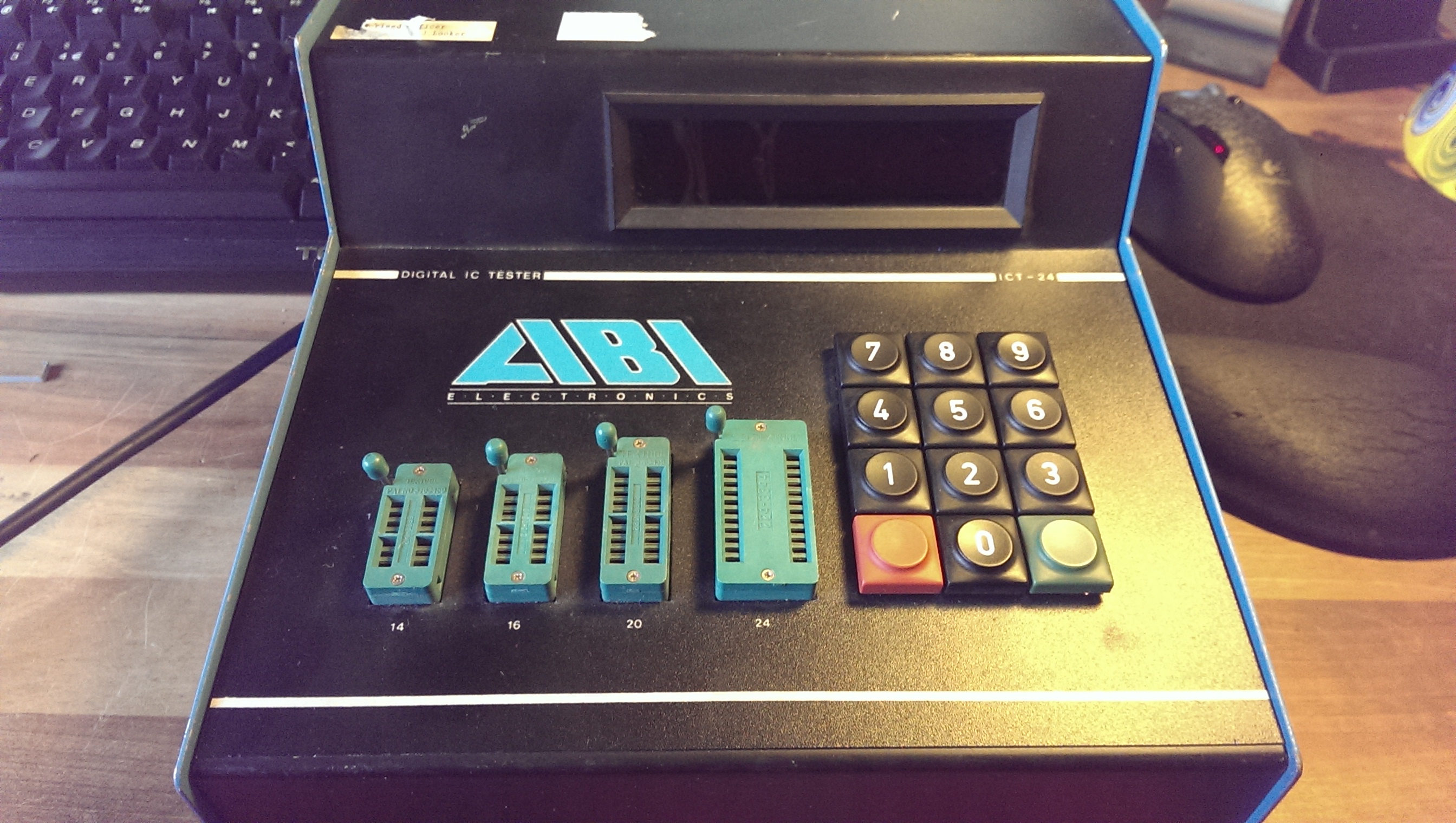
I recently found one of these devices and being a lover of test equipment I decided to see what it was all about.
IMAG1835

There is very little information about these online. The only official mention I can find about them is on ABI’s website and it just makes a passing reference to it stating it was the first IC tester device they made.
All other information comes from Equites who has had one of these for a number of years now. He has dumped the ROM’s from his unit and they are available in the downloads section.

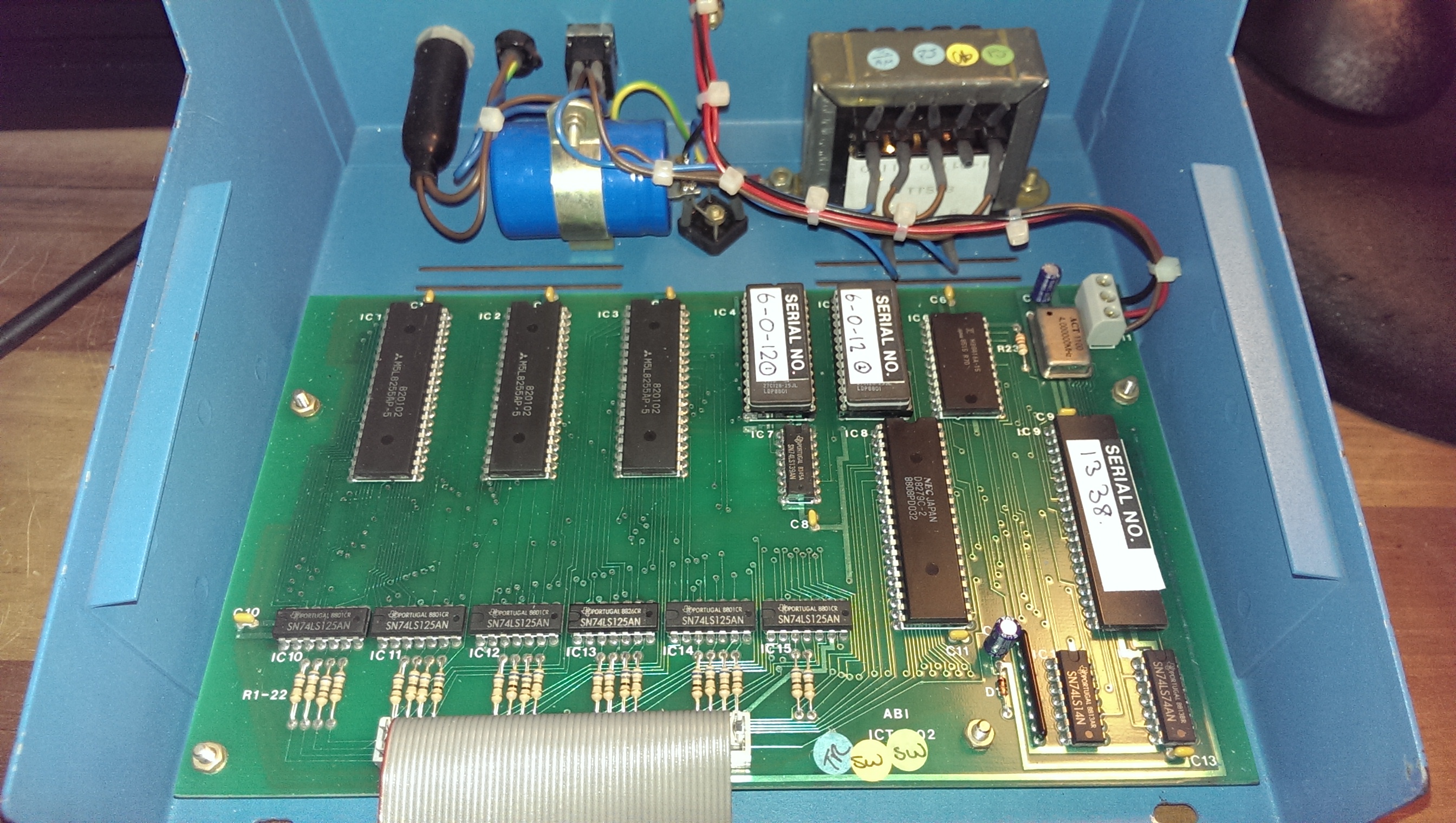
So, I got my unit and powered it up to make sure it worked. Once I had confirmed that I opened it up.
IMAG1837

I could see straight away that I have a different firmware version, mine being 6-0-12 and the version Equites has was 5-9-12. I’m still not sure what the difference between the two is.
So I dumped these EPROM’s (available in the downloads section too) and created a schematic for the unit.
The device is a Z80 based system with a couple of EPROM’s, a RAM chip, a keyboard/display interface chip and three PPI chips to control IO reading/writing.

Once I had drawn it out I derived the following memory map
$0000-$3fff – ROM1
$4000-$7fff – ROM2
$8000-$87ff – RAM

8255 (IC1)
$c000 – PORTA
$c001 – PORTB
$c002 – PORTC
$c003 – Control

8255 (IC2)
$c004 – PORTA
$c005 – PORTB
$c006 – PORTC
$c007 – Control

8255 (IC3)
$c008 – PORTA
$c009 – PORTB
$c00a – PORTC
$c00b – Control

8279 (IC8)
$c00c – Data
$c00d – Control

IC1 – Controls the /OE lines to all the IO buffers
IC2 – Controls the inputs the the IO buffers
IC3 – Controls the reading from the ZIF sockets

The ROM’s, RAM, 8279 and 8522 chips enable lines are controlled via 74LS139 decoder chip.

The version number of the firmware can be displayed by keying in “005” on the keypad.
On my version it displays “6-0-12” which matches the labels on the EPROM’s.
Interestingly the “6-0” is stored as data in the ROM while the “-12” is hardcoded as instructions starting at $11cd.
The first 2 digits, in my case “6-0” represent the software version.
The remaining digits are the options installed. Mine as options 1 and 2 installed.
Option 1 is for memory devices
Option 2 is for interface devices

The unit does a power on self test which displays a fault code between 0 and 6. These may be explained in the manual which I don’t currently have so I took apart the disassembled code to see what they meant.

Fault 0:
One of the IO’s is tied to GND.
The software tristates all the IO pins via IC1 (8522) and reads them back via IC3 (8522). They are held at logic HIGH via a pull up resistor network. If any pins are low this will result in FAULT 0.

Fault 1:
One of the IO’s on PORTA is tied to VCC.
The software sets all of the IO pins on PORTA to logic LOW and reads the states back. If any pins are found to be logic HIGH on PORTA then this will result in FAULT 1.

Fault 2:
One of the IO’s on PORTB is tied to VCC.
The software sets all of the IO pins on PORTB to logic LOW and reads the states back. If any pins are found to be logic HIGH on PORTB then this will result in FAULT 2.

Fault 3:
One of the IO’s on PORTC is tied to VCC.
The software sets all of the IO pins on PORTC to logic LOW and reads the states back. If any pins are found to be logic HIGH on PORTC then this will result in FAULT 3.
NOTE: The 2 uppermost bits on PORTC are not used for reading back IO lines.

Fault 4:
Fault with the program RAM.

Fault 5:
Fault with display RAM.
RAM should be 0x0. If it is not then FAULT 5 with be displayed.

Fault 6:
Fault with display RAM.
RAM should be filled with alternating 0x55 0xAA. If these values are not correct then FAULT 6 is displayed.

Equites supplied me with some additional pictures and a manual for these units and apparently there is a rebranded RS version too.
That’s about it. I have commented a lot of the code and learnt a great deal about how it works.
Its a very robust unit and no doubt it will get some use despite having other methods available to test. Its much more appropriate to have in a garage workshop.

If anyone can offer any further information about this (or feels the need to emulate it) then please get in touch.
Thanks to Equites for his information and scans.

 Posted by at 1:14 pm