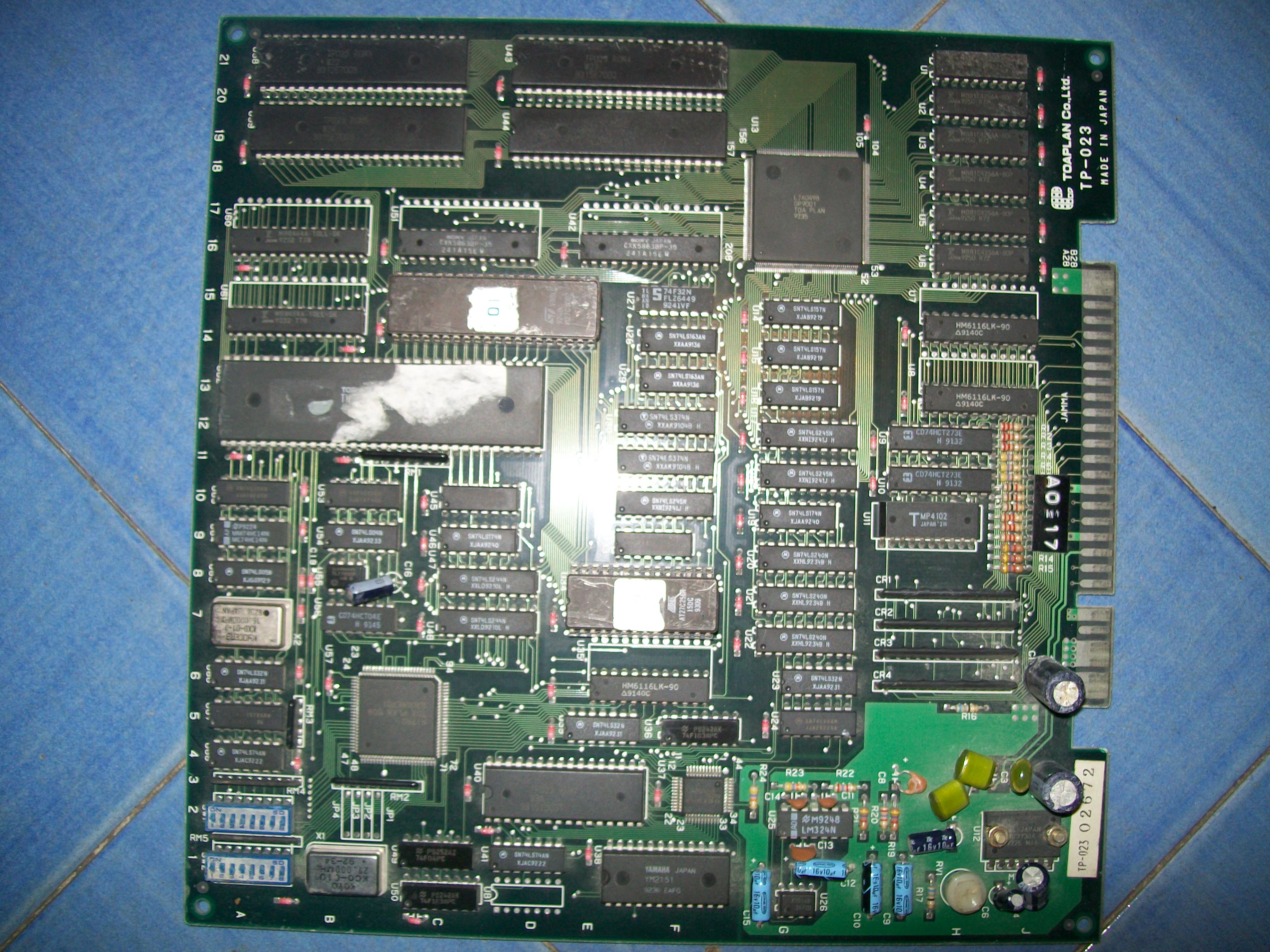
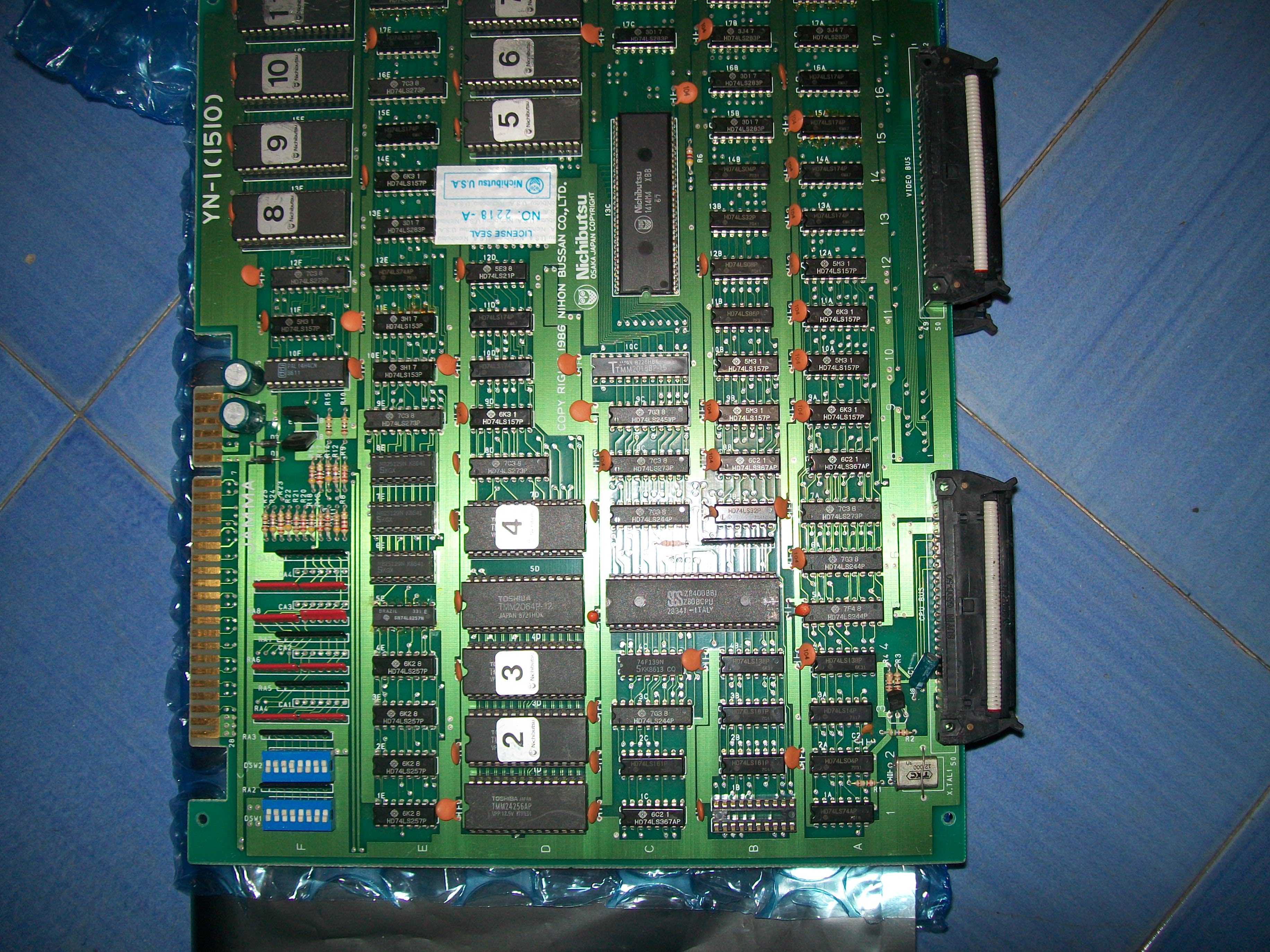
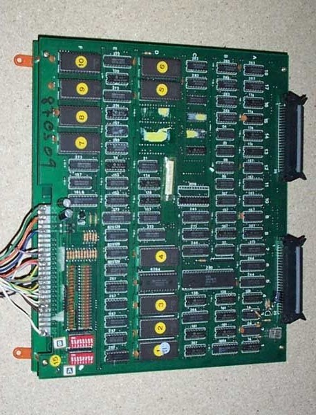
I’ve been working with a Popeye PCB recently and I wanted to figure out the hardware so I thought it would be good to document what I found.
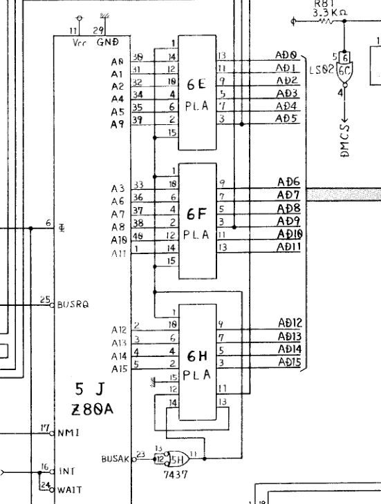
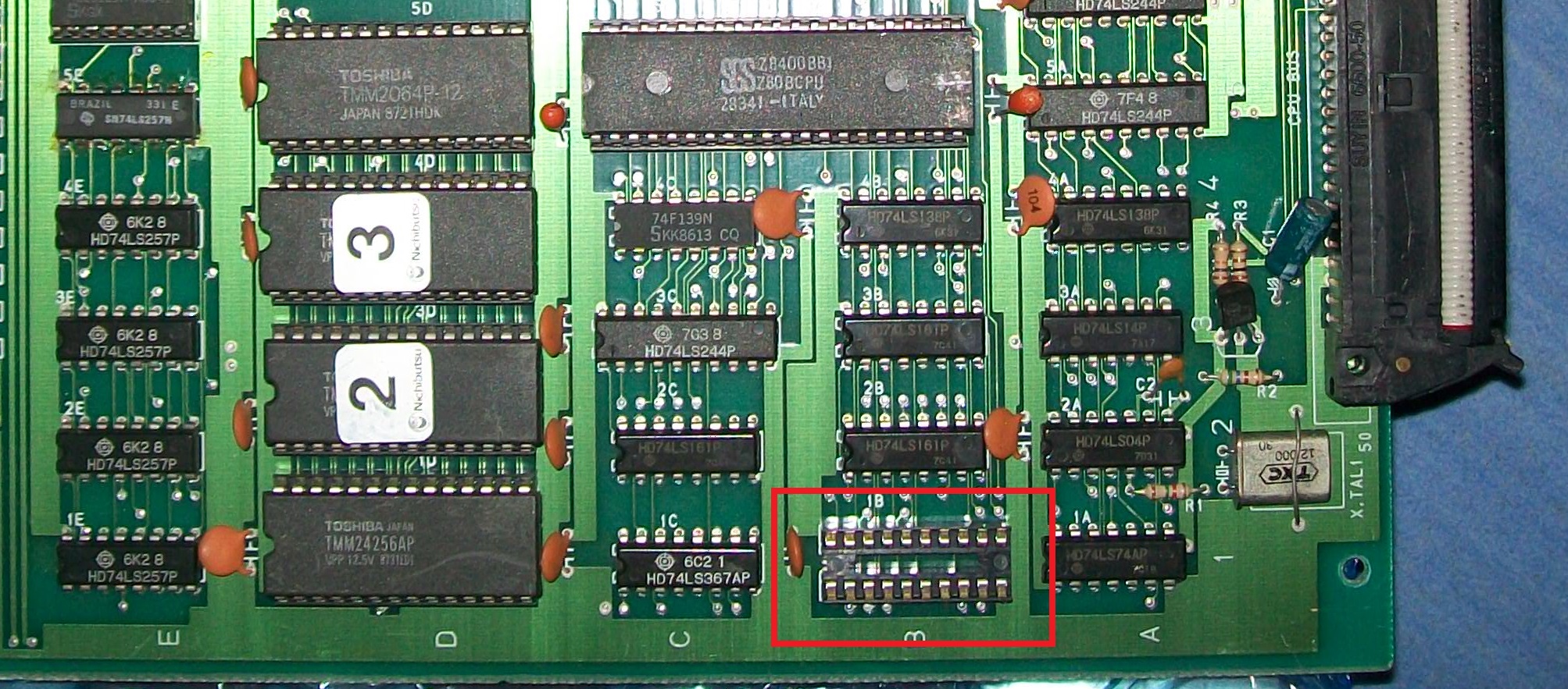
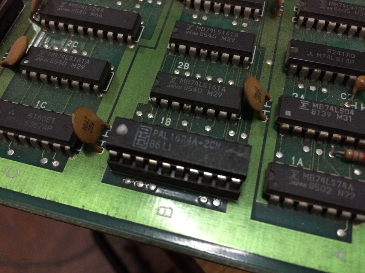
The PCB uses some fairly simple obfuscation for the CPU address lines utilising what the schematics refer to as a PLA device. Further investigation revealed that the devices used on the address bus here are actually 74LS367 at locations 6F and 6H. I originally believed the IC at location 6E to be the same but in the decoding routine that MAME uses, the new address value returned after swapping the bits gets XOR’d by 0x3F.


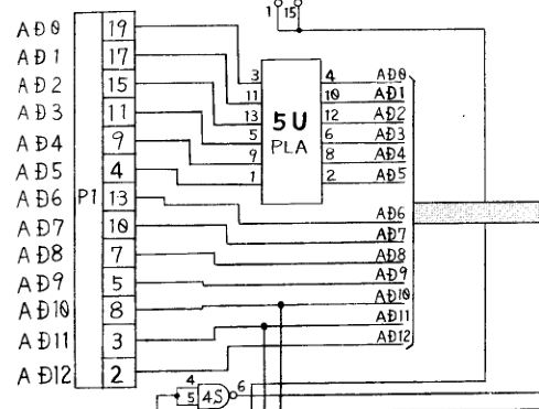
Checking further I found this chip is actually a 74LS368 (inverting line driver). If you notice on the video PCB there is another chip with its markings removed at location 5U.

This is a 74LS04 inverter and is needed because the lower 6 address bits are inverted from the CPU by the 74LS368 at location 6E so we need to return them to their intended state. Inverting them again allows the video and background RAM to be addressed properly.
All these so called PLA’s are actually regular TTL with their markings etched off.
The data lines are also scrambled and can be easily followed from the schematics.
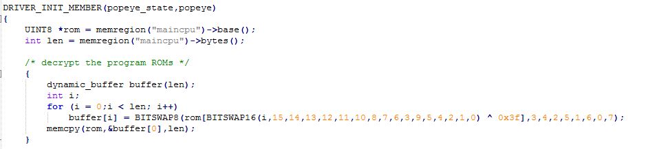
The code in the program EPROM’s is scrambled to accommodate the above methods.
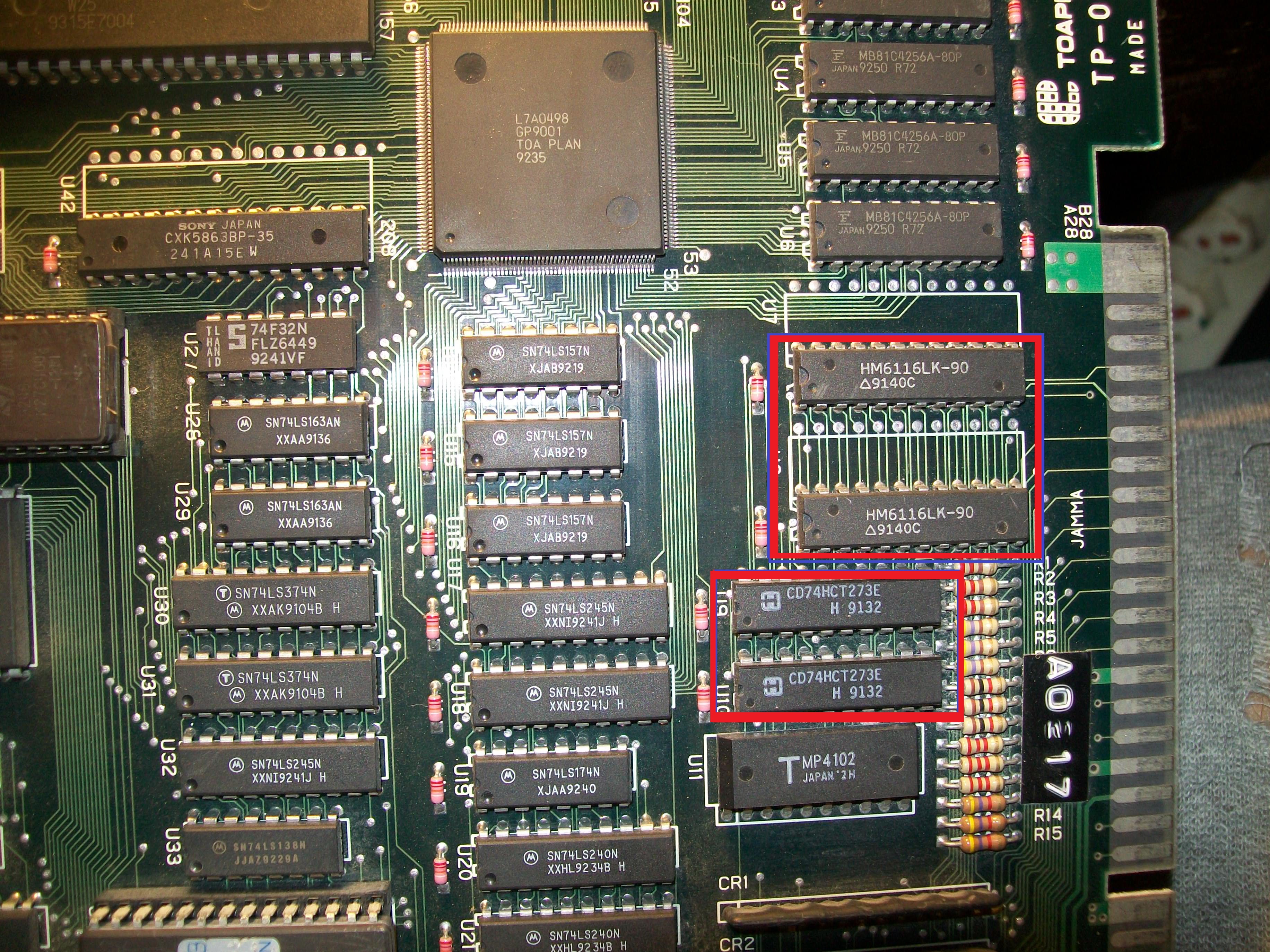
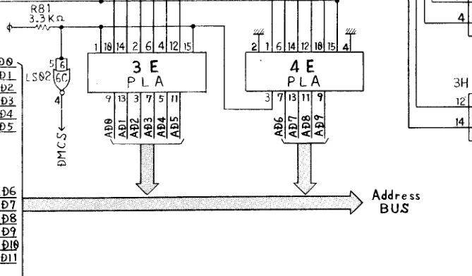
There are 2 additional IC’s also marked as PLA’s attached to the outputs of 3 x 74LS161 counters at location 3E and 4E. These have been identified as a 74LS365 at location 4E and a 74LS368 at location 3E and are part of the DMA circuit.

NMI
The hardware doesn’t use any other interrupts, only the NMI.
The NMI vector is the same for all Z80 program and starts at address $66 in ROM.
It is triggered essentially by the /VBLANK signal and during this time all the on screen background and sprites are updated.
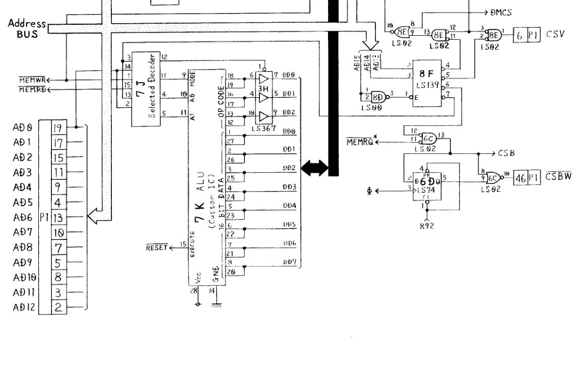
MAIN RAM
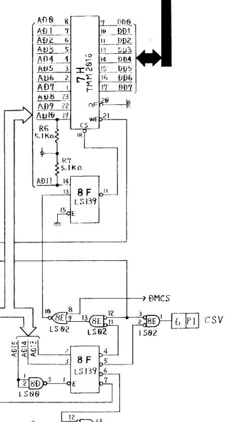
The main RAM for Popeye lies at address $8800 – $8FFF and is a TMM2016 located at 7H on the CPU PCB.
The main RAM doesn’t appear to invert the lower 6 bits of the address bus so the actual locations written to in RAM will be different to what the program actually expects however this is not an issue as all the accesses will give the correct data. In the event of fault finding though this could potentially cause confusion.
DMA accesses to this RAM are all correct.
Access to this RAM is controlled via a 74LS139 at location 8F.
The first demultiplexor of this IC is enabled when address bit A15 is HIGH (address $8000). Output Y0 connects to select input B of the second multiplexor and address bit A11 is connected to select input A. Output Y1 (pin 11) is connected to the /CS pin of the RAM.
In order for Y1 to be active A15 and A11 need to be HIGH (address $8800).

There are two pull-up resistors used on this RAM connected to AD10 and AD11. These are present for when DMA accesses are happening as it only uses 9 bits. Without these resistors AD10 and AD11 would be floating during these times.
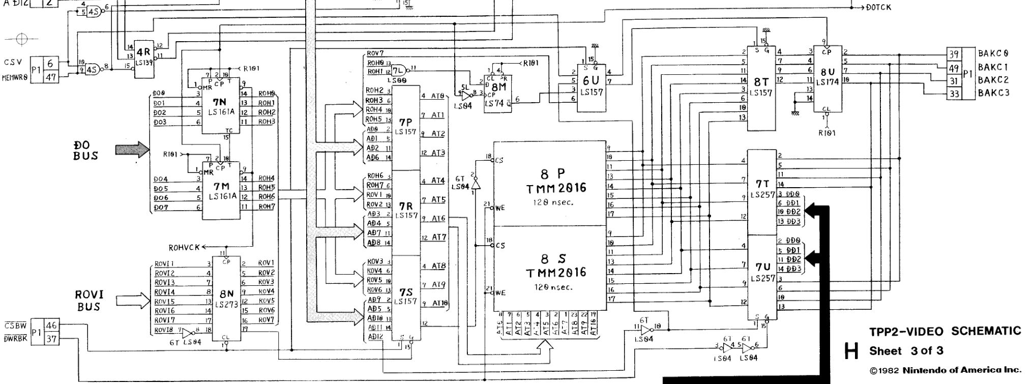
BACKGROUND RAM
As we only write nibbles to the RAM section but need to preserve the nibble value we currently are not writing too there is a system in place to deal with that.

/CSBW is generated when we write to anywhere in address $C000 – $CFFF.
This signal clears the DMA access to background RAM and sets the 74LS157 chips to use the address bus instead of DMA.
When a write to the background RAM is initiated the 74LS174 at 8U gets clocked before the write enable for the RAM goes low. This latches the current RAM nibble not being written to, onto the outputs of 8U which lets the RAM get updated without losing data.
The delay for latching the RAM data before writing is achieved by a 74LS20 at 5D on the CPU board. One of these signals is the /WR but goes through a 74LS74 in order to create a delay of 1 clock cycle. This gives enough time to latches the RAM data before the write enable is active on the RAM itself.
SECURITY ALU
There is a security ALU that sits at address $E000 – $E001 in the memory map. It can be both read from and written to. MAME has functional behaviour for this emulated in the driver.
The various modes of the ALU are selected by an IC labelled as ‘Selected Decoder’. This is actually a 74LS139.

I wanted to implement this chip into one of the 28 pin CPLD modules I have. Being an amateur in HDL programming I wasn’t too sure whether the design could be implemented into an unclocked CPLD design so I asked my friend Charles MacDonald for some advice on Verilog.
He kindly sent me a draft code based on the MAME implementation. I have adapted this to reflect the real hardware and it is now implemented and seems to be working. The programming file can be found in the download section if anyone ever feels the need to use it. I would still like to get hold of an original chip to study as although the code for this works with the titles that use it, all the behaviours of the chip are not fully documented that I know of.
Without this chip present Popeye will reset when starting a game. There may be other issues as well but I cannot pinpoint them.
There is an unprotected version of Popeye available in MAME which does away with the requirement for this security chip so there isn’t much need to use a reproduction of this chip.
UPDATED 10/03/2019 – Ace’ informed me of an error. 4E is actually a 74LS365 NOT a 74LS367 like originally stated.