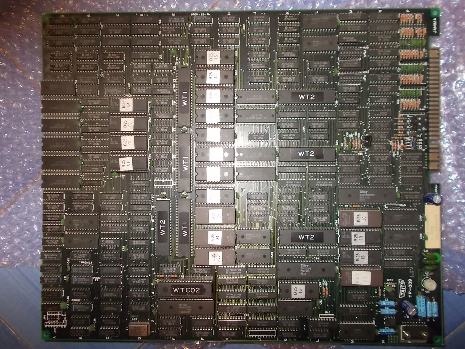
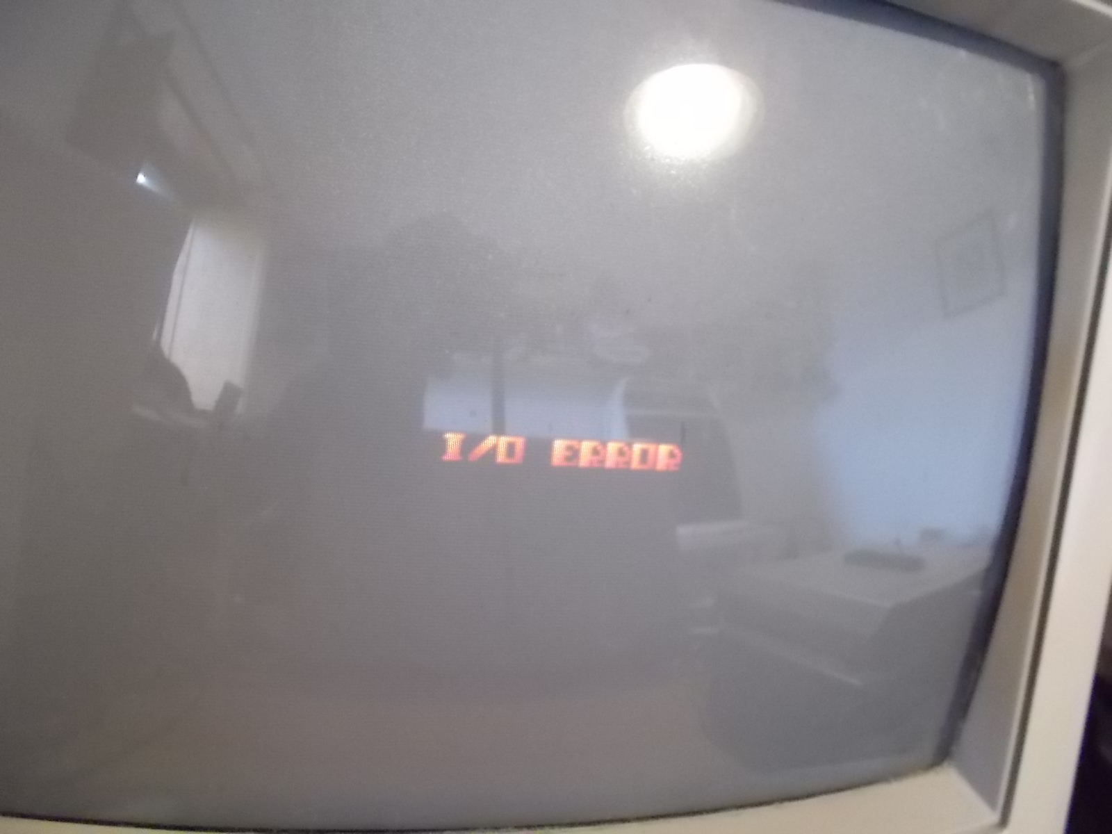
Jun 012016
 

Initial Symptoms

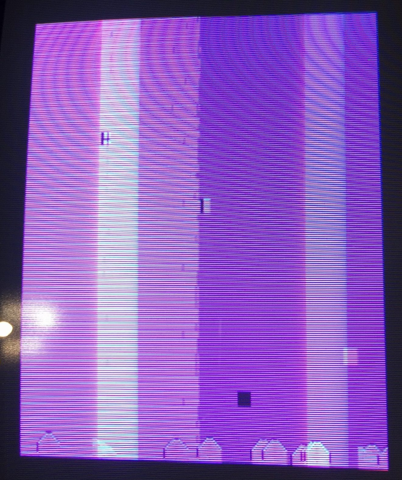
  • Static junk on screen, which changes between reboots.
  • No sound or evidence that game is running in background.

Sony PVM monitor wouldn’t sync in RGB mode, but would (for some reason) in Y/R-Y/B-Y mode.

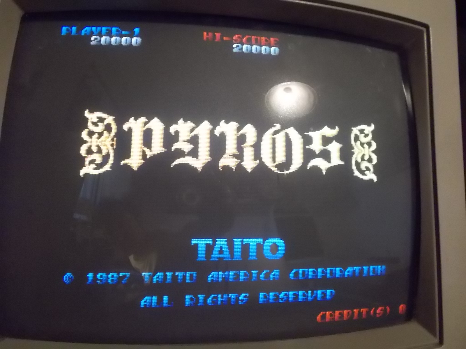
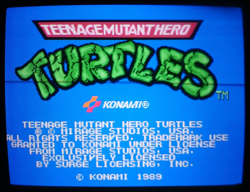
Random junk when powered on

Random junk when powered. (purple image is due to monitor problem)

CPU Boot Problem

Probing CPU interrupts showed that sometimes V-Blank interrupts were active, sometimes not. Initial check of EPROMs showed that one was dead, but replacing did not solve the problem. Probing with a logic analyser showed that the data/address bus of the main CPU was pulsing, and the game wasn’t watchdogging so deeper investigation was required.

Tracing with a Saleae logic-8 showed that the first v-sync interrupt was getting acknowledged by the CPU, but subsequent interrupts were ignored. Digging futher I generated a partially complete address/data trace by the (shared) data+address bus and the bus status lines (BS0-2). Since my analyser is only 8-bits, I could only trace 5 data+address lines at once. I wrote a script to combine multiple traces using the bus status lines to synchronise the data. Luckily the behaviour was deterministic, and I could extract enough trace data (12-bits of both data and address) to work out a full trace by correlating the data with a mapped ROM dump from Mame. Doing this I found that one of the RAMs was faulty; The stack was getting corrupted, causing a ret instruction to jump to an unexpected program address. Swapping the program RAM resulted in the game booting.

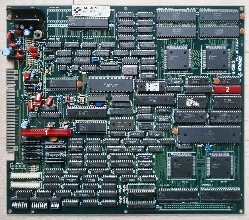
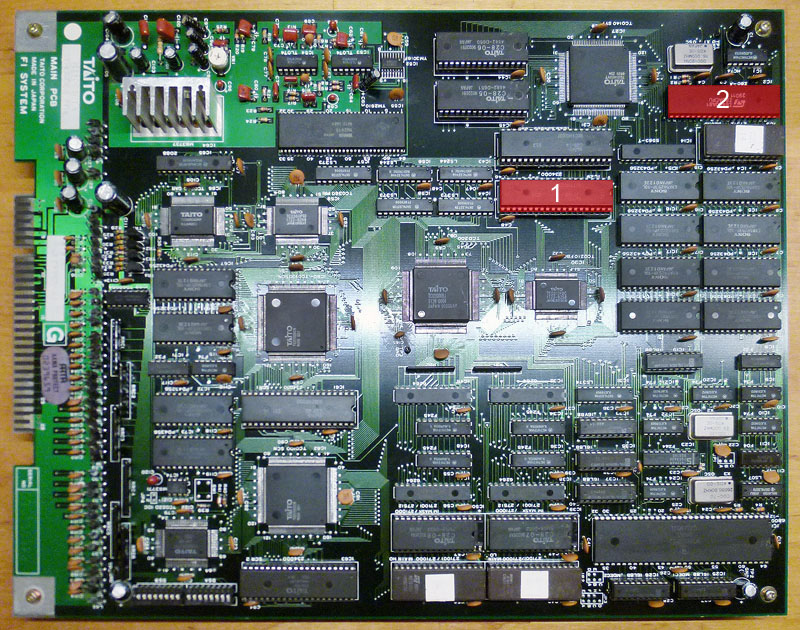
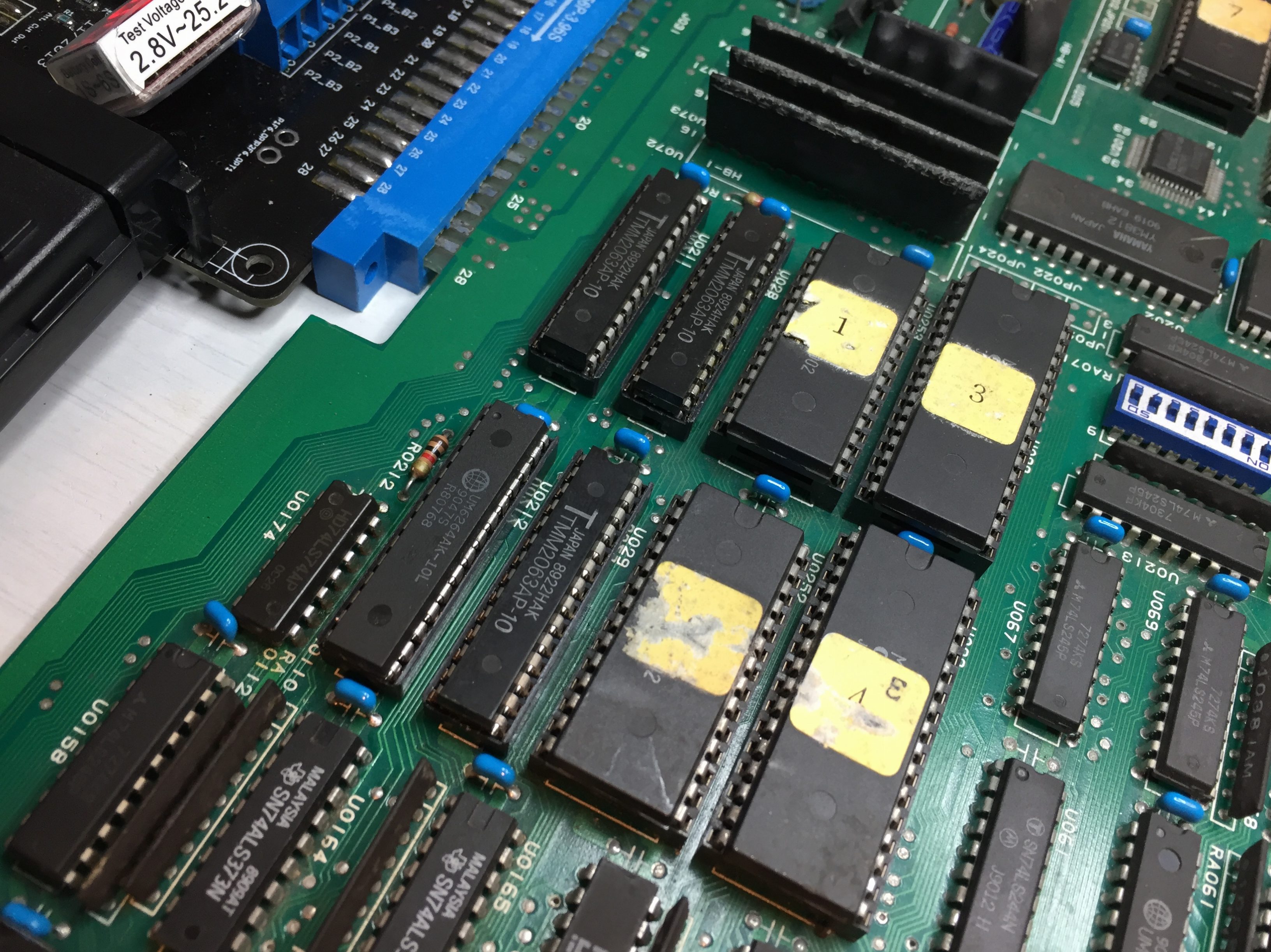
Bad SRAM of main CPU. Socketed and replaced.

Bad SRAM of main CPU. Socketed and replaced.

New Symptoms:

  • Some tiles have flickering horizontal bars
  • Some tiles seem to not change from top to bottom (in horizonal screen)
  • Sound crackly and missing music
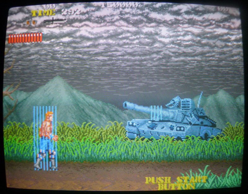
Background tiles are corrupted

Background tiles are corrupted

Tile Corruption Problem

Probing the tile ROMs shows that ROM U105 address lines 1-4 were floating. These were driven by the SEI0020BU custom chip at U102. Pulling the SEI0020BU and swapping it with it’s neighbour switched the tile corruption. Clearly the SEI0020BU was the cause of the problem. Annoyingly these aren’t easy to come by.

Reverse Engineering the SEI0020BU

I guessed that the main function of the SEI0020BU was to drive the addresses of the ROM chip in the direction of the raster. I checked the connections of the SEI0020BU with a multimeter and worked out the function of each pin (see schematic below for more details).

Checking the Mame source confirmed that the address mapping for this chip corresponded with the x-axis scroll register. I guessed the purpose of the chip was to store an x-axis scroll offset and add that result to the raster x-position. I guessed that only 8 bits of shift were actually needed, and I knocked up a prototype on a breadboard, which seemed to work well.

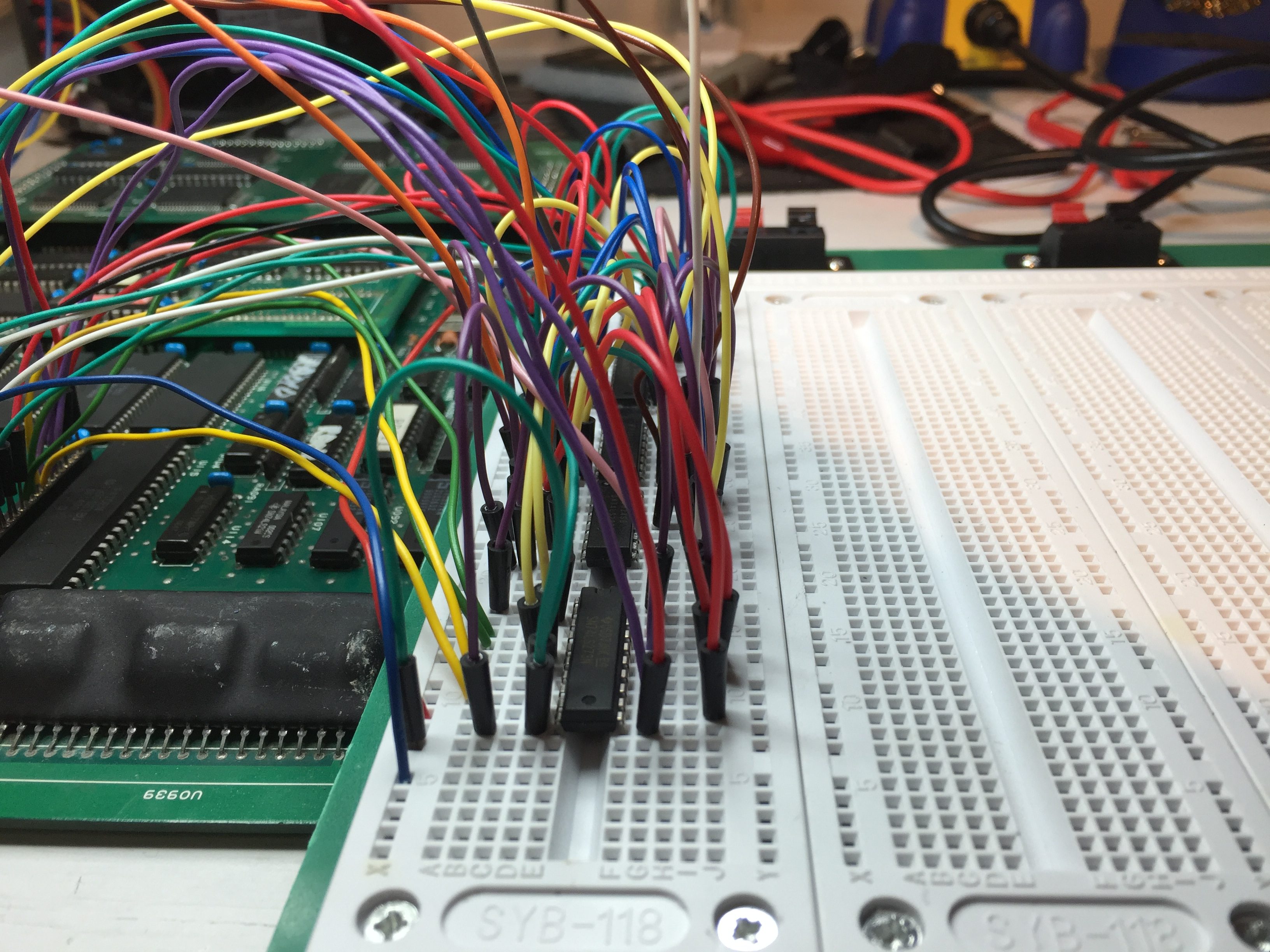
SEI0020BU breadboard prototype

SEI0020BU breadboard prototype

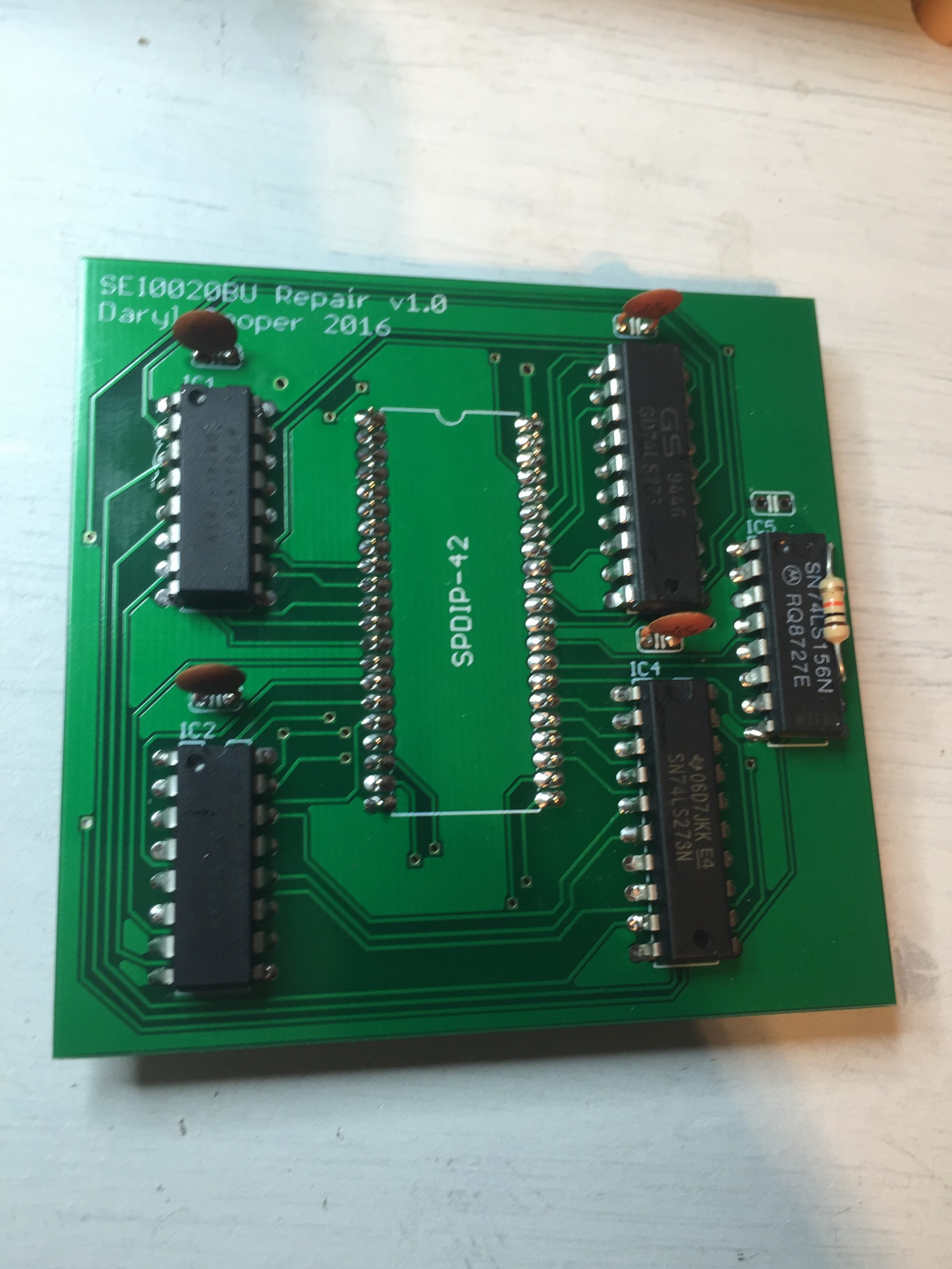
With a working prototype, I got to work using CadSoft EAGLE (PCB CAD tool) to design a PCB daughterboard for a more permanent solution. The PCB was printed by Seeed, and delivered in a few weeks.

First SEI0020BU daughter board

First SEI0020BU daughter board

Once the printed PCBs were delivered, they seemd to work well, but I’d made a few mistakes. Firstly, the output from the LS156 should have been pulled high. Secondly, only 8 bits for the shift offset was insufficient – I actually needed 9 bits. This was a stupid mistake – I’d been unable to test the full shift range properly on my test rig because of a faulty joystick adaptor! Once I tested the board in a cabinet, it was clear that scrolling too far to the left (offset register wraps) causes the tiles to distort (-1 wrapped to 255 instead of 511).

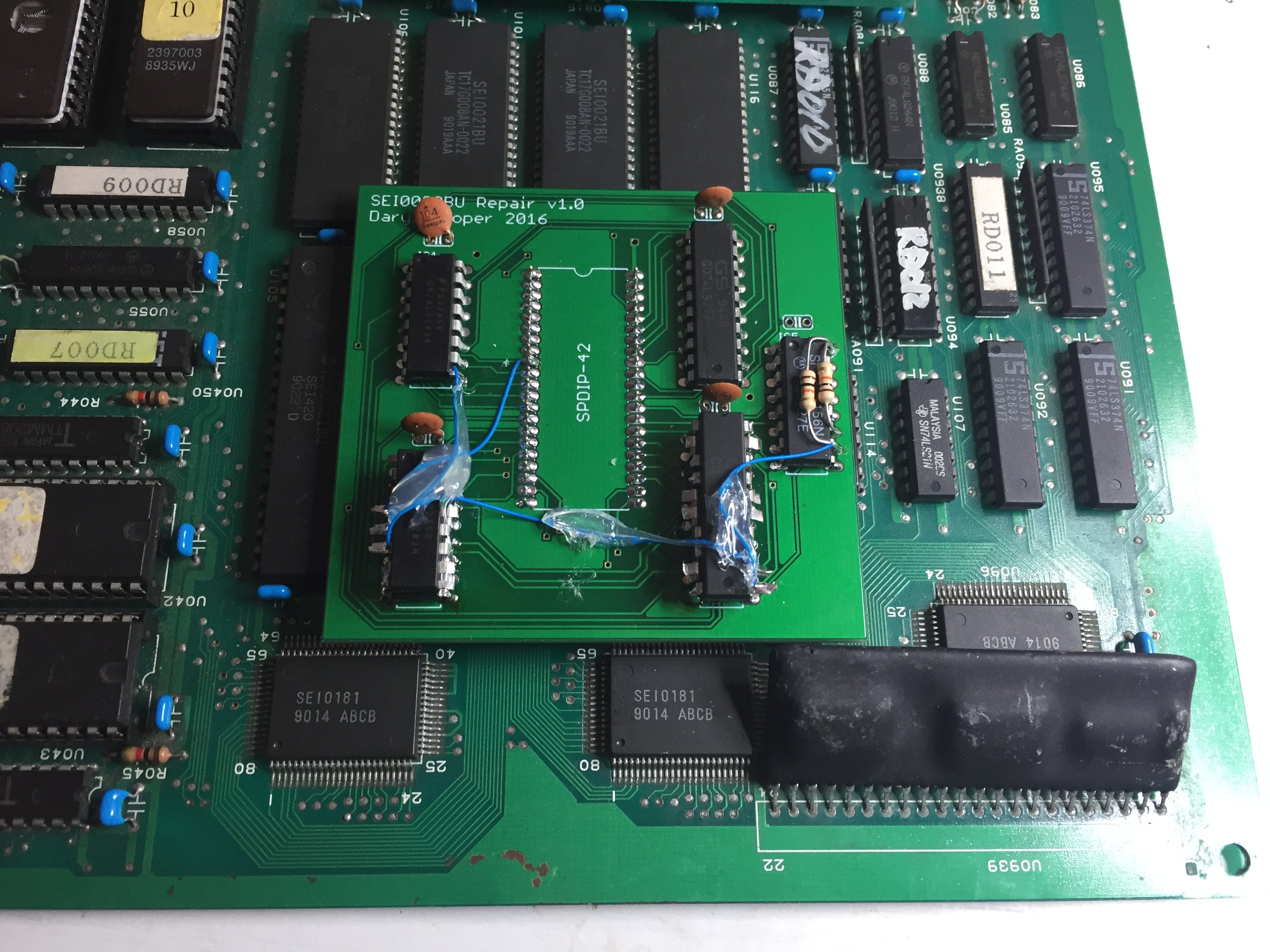
I managed to hack a fix onto the PCB by piggy backing an extra 8-bit buffer and a 4-bit adder onto the PCB, cutting a trace and wiring up with patch wires. The modified PCB finally worked properly, and the graphics were fixed. I wasn’t happy with it though – I’d printed a PCB, so I thought I may as well finish the job!

Patched SEI0020BU Replacement Daughterboard

Patched SEI0020BU replacement daughterboard

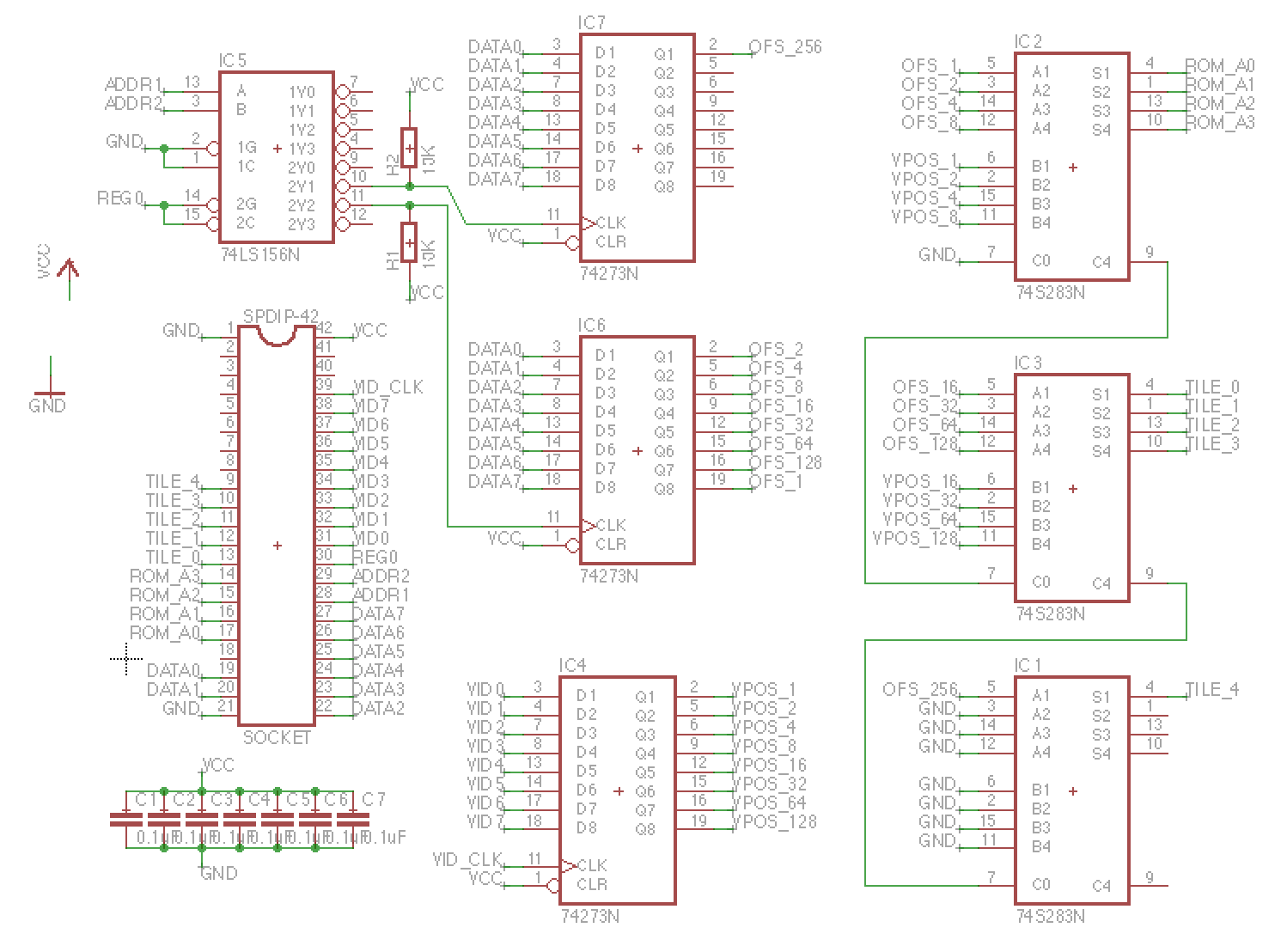
I modified my design in Eagle (see schematic below), and ordered a new set of PCBs to be printed.

SEI0020BU Schematic

Schematic for Raiden SEI0020BU replacement

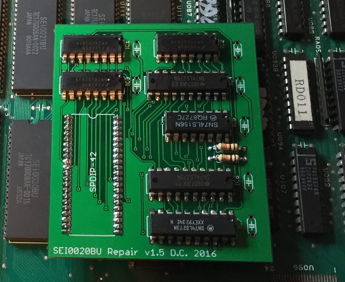
The new PCBs arrived, and worked perfectly – phew!

Final working SEI0020BU replacement daughterboard

Final working SEI0020BU replacement daughterboard

Sound Fix

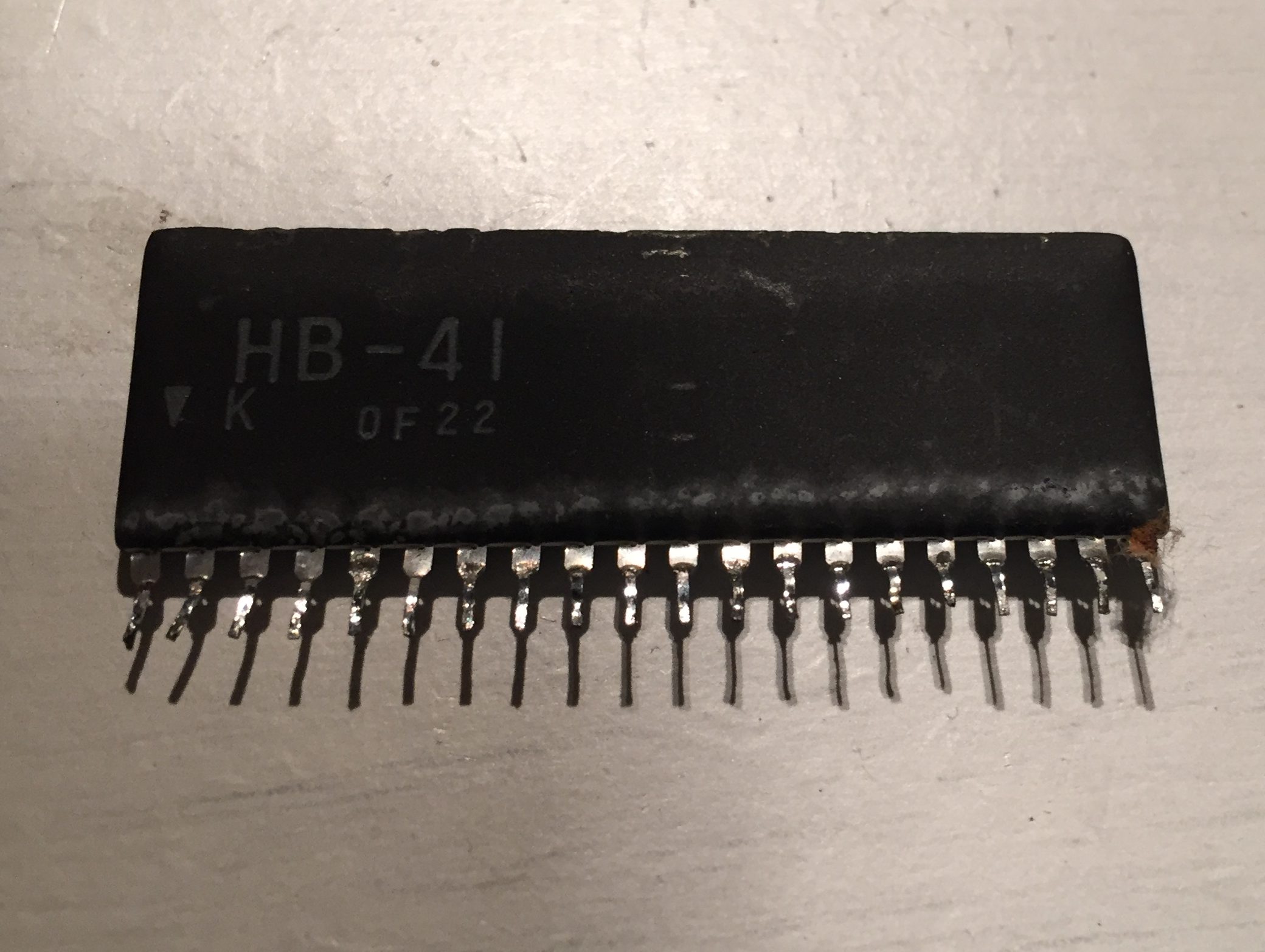
Sound was working, but distorted and noisy. Probing the sound input to the amplifier with an oscillioscope showed that the signal was weak. This was driven by the HB-41 SIL package. The inputs to the HB-41 looked clean, so it looked like it was bad.

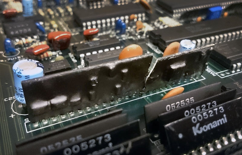
Faulty HB-41 SIL package

Faulty HB-41 SIL package

Luckily I had a spare on a Seibu Soccer donor board. Hooking it up solved the sound problem. Job done!

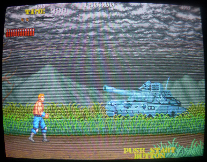
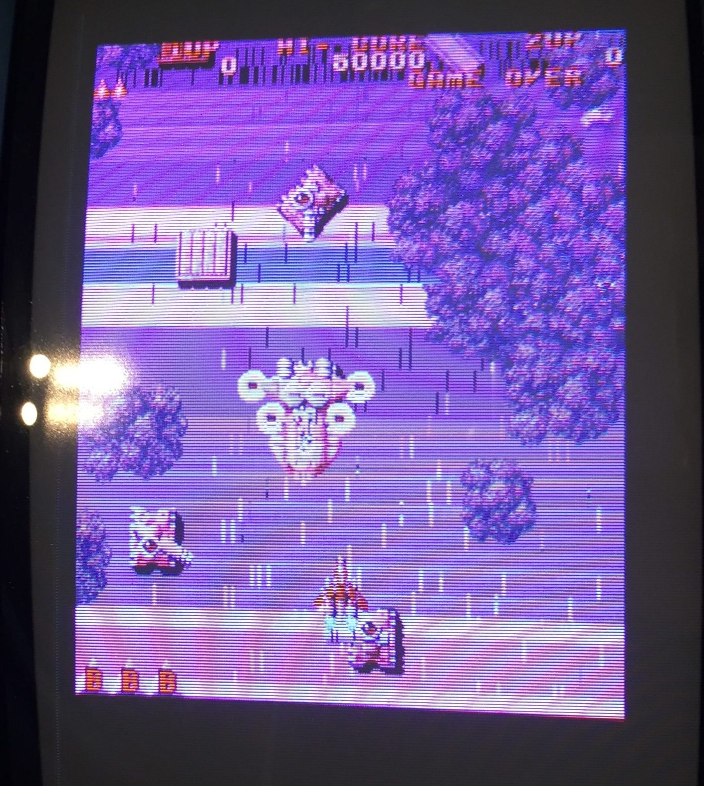
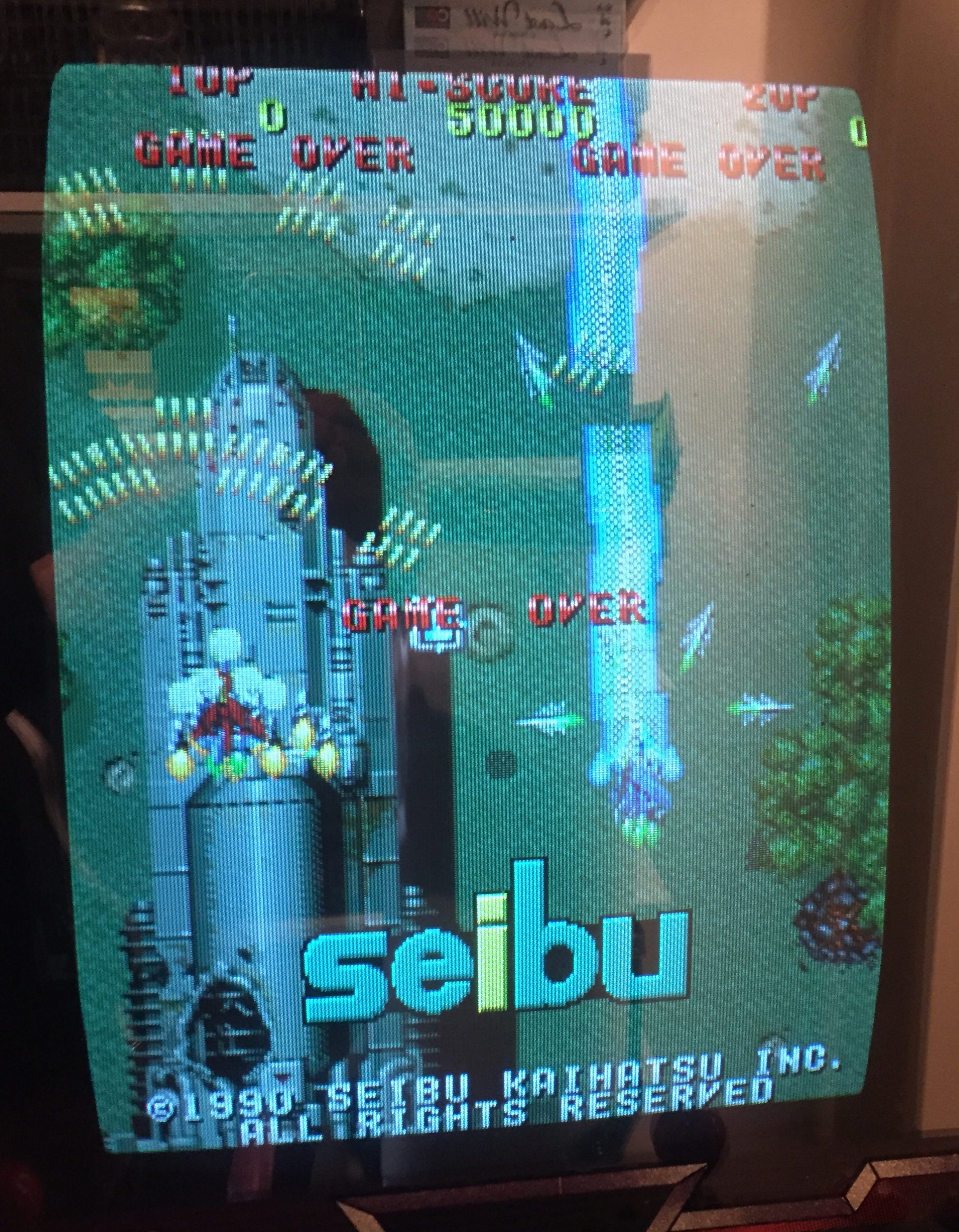
Image is clean, and game now functions correctly.

Image is clean, and game now functions correctly. Colour correct in arcade cabinet.
Polar Toneohm 850 repair log

 Equipment Repair Logs  Comments Off on Polar Toneohm 850 repair log
May 282016
 

Last week I bought on Ebay an untested Polar Toneohm 850 (picture from Internet) :
For the uninitiated this is a instrument that is able to locate quickly and accurately shorts on PCBs.Device is essentially an audible milliohmmeter which, indeed, produces a tone whose frequency is inversely proportional to the resistance measured across its probes.The more you get closer to the short  and so the lower will be the resistance, the higher will be the produced tone.This is very useful when you come across a PCB with a dead short or small resistance between VCC and GND, using a normal multimeter would have no effect since you will end up to measure always same resistance values due its accuracy (most if times of 0.1 ohm ) which is too coarse.

So, I bought this kind of equipment which arrived me a couple of days ago.When I saw the package, I immediately had a bad feeling :

DSCN3315

The box was broken and, once opened, the case of the unit too:

broken

But worst , the unit didn’t power on at all, it was competely dead while the seller clearly stated (sending me also a picture)  that, although untested, instrument turned on showing numbers on display.

Since I needed this piece of equipment I opted for repairing it instead of asking for a refund and send it back.

I opened the unit and PCB was in untouched state, no sign of damage or burn components.DSCN3328

First of all I went to check voltages on the various test points, I could only measure few Millivolts.Thanks to the user ‘Fraser’ (thanks again!) on EEVblog forum I got schematics of this specific model so I could start my troubleshooting more confident.Design of the unit is quite simple : the 220VAC ( unit came with 120VAC line selected so  had to change it accordingly to my country) reaches the main transformer ‘T1’ being reduced to 9VAC then it got rectified by a couple of bridges and then regulated by a 7805 and  couple of 78L05 providing power for all the logic :

PSU_circuit

Again, I was able to measure more or less +1V on the inputs of the tree voltage regulators so problem was upstream, specifically in the main transformer (‘T1’ on schematics) :

T1_transformer

Said simply, a transformer is a device made of a primary winding  and one of more secondary windings.Windings are usually wound around very high permeability ferromagnetic cores.A varying current in the transformer’s primary winding creates a varying magnetic flux in the core which is transferred to the secondary windings by magnetic induction.

So, my problem was clearly located in the windings.I removed the transformer:

T1_removed

I went to check windings with my multimeter and none of them gave me resistance values, they were almost all opened due the shock received during shipping!But luckily they were interrupted just near the pins, see picture of primary ones for example :

primary_windings_broken

A bit of ‘surgery’ was needed using some AWG30 wire to restore all connections (part in excess of wire was cut, obviously)

primary_buildings_rebuilt

Once mounted the transformer and reassembled all the pieces, the unit came back to life fully working!

fixed

Video below shows a testing on an arcade board where a 100nF by-pass ceramic capacitor was intentionally shorted:

 Posted by at 10:43 pm

Splatterhouse repair log #4

 PCB Repair Logs  Comments Off on Splatterhouse repair log #4
May 262016
 

I got from New Zealand this genuine Splatterhouse PCB for a repair:

Splatterhouse_PCB

Upon boot the board was stuck on a “ROM TEST START !! PLEASE WAIT…” message displayed upside down :

issue

From my past experience I know for sure this issue is caused by a bad ’64A1′ custom replaceable with a programmed Hitachi HD63701 MCU (plus a patched ‘VOICE0′ ROM in order to handle two custom opcodes of the ’64A1’)  following this procedure:

Namco System 1 custom ’64A1′ replacement

But in this case, as you can see from the above picture of the board,  the owner already replaced the ’64A1′ (and at same time  patched the ‘VOICE0′ ROMs using an hacked 1Mbit JEDEC EPROM in place of a non-JEDEC one ) and this didn’t fix the issue.For first I reverted the modification the and reinstalled the original custom ’64A1’.With this configuration the board successfully booted into game although some sound samples were bad.This lead me to think that there could be some problem is the data bus of the VOICE ROMs which prevented the HD63701 MCU to correctly read the patched data causing the missing boot. :

VOICE_ROMS

So, assisted by schematics, I went to check the involved circuit and found that pin 20 (data line D6) of the VOICE ROMs (Splatterhouse use only four of them to store samples) was not daisy-chained as it should have been:

VOICE_ROM_DATA_BUS

In the above snippet of schematics you can see (red mark) where extactly trace was interrupted.I simply used a bit of AWG30 wire to restore comnection:

patched_PIN20_VOICE_ROMS

This fixed completely the game using both the original ’64A1′ custom and the HD63701 MCU.End of job.

 Posted by at 8:19 pm

Sharp SF-1 (SNES TV) repair log #2

 Console Repair Logs, Repair Logs  Comments Off on Sharp SF-1 (SNES TV) repair log #2
May 222016
 

The 14″ TV is up now.
This one was a lot more involved.
Before starting on this one I had tested the previous PCB with this TV so I knew for sure the TV part was operating fully.
sf1-repair

When powering this up I got no audio or video, just a black screen. Using the external A/V output also gave me nothing.
I couldn’t find anything obvious visually on the PCB itself.
Ive read a lot in the past about SNES repairs and the CPU’s seem to be a weak point. I started prodding around the CPU with the scope and even though all the voltages and clocks looked good I could see any activity.
I had a known working spare SNES which I opted to sacrifice for parts.
sf1-pcbmark

I replaced the CPU and once again checked for signals. This time I had life but it gave up after a few seconds and still didn’t give me any output. This cycle was repeatable on resetting the machine.

I next opted to replace the ‘S-WRAM’ (work RAM) positioned next to the CPU.
Replacing this gave me audio but no video so at least I knew the game was running which was great to hear.
At this point I tried the external A/V connector again and got a good picture.

Probing the ‘S-Enc’ chip yielded no outputs at all despite all inputs being as expected. I replaced this and everything came up good. Time to reassemble and reclaim some bench space.
Thats both of these rare units fixed up.

sf1-pair

 Posted by at 10:21 am
May 212016
 

A couple of friends were looking to get their SF-1 SNES TV’s repaired. Not one for letting such gems go to ruin I offered to try and help out.
There were two units in need of repair, a 14″ and a 21″.
sf1-top

This log will focus on the 21″ version first.

On power up with a game fitted I got audio and a very faint greyed out picture.
I had been given an RGB scart cable with these so as they have the standard A/V output port on them I thought I’d give that a go.
I got this
sf1-sync

As you can see the sync signal is off but I could see a nice colour picture. This gave me initial hope that the PPU’s were not to blame for the grey faint picture.
Taking this unit apart was a bit of a pain with the SNES part being sandwiched in at the top but I got it out and looked for anything obvious.
sf1-pcb

(Note that this PCB image is actually from the 14″ version. The 21″ version has a very similar PCB with only the connector location being located differently. I forgot to take a picture of that one.)

There was nothing obvious so start looking at the missing sync signal first.
The answer was fairly straight forward. The RGB cable I have here uses the composite signal for its sync. The SF-1 does not seem to output a composite signal at all instead it uses the combined HV sync signal on pin 3. Hooking this up instead gave me a nice picture on my test monitor which confirmed the SNES was working great.
So whats happened to my picture on the actual TV unit?
It turns out the SNES outputs separate Luma and Chroma signals to the TV for its picture and not RGB like we initially thought.
sf1-connectors

The connector marked ‘VD’ is the video signals. The black wires are all grounds and the white wires are signal. One of the wires however is the audio output. So there is Luma, Chroma and mono audio on this connector.

Now I know the signal isn’t RGB I can pretty much assume that the ‘S-ENC’ (BA6952F) is used to generate the signals i’m missing.
Using the scope I couldn’t find any valid signals coming from the chip. In my haste I was about to write the chip off but as the output signals were really weird I traced all of the pins. I found the GND on pin 2 wasn’t connected at all and it should have been. I tried reflowing the pin but still no connected so I added a jumper wire to the GND point next to it.
20160518_205235

I was a little nervous about patching it as if the original track (that ran under the chip) had burnt out then what had happened to do that? It could have been a manufacturing defect, Ive seen a couple of those in my time but ground connections are generally quite big compared to signal traces. I didn’t want to remove the whole chip just to check for a burnt trace so I just check resistance between GND and VCC. It looked fine so I powered up to test.
21picture

An absolutely perfect picture! Seriously this picture is really good quality.
I tested all the controls and they seem to work fine too so time to box this up.

 Posted by at 8:18 pm