This repair log is proof that we must always start from the simpliest things!
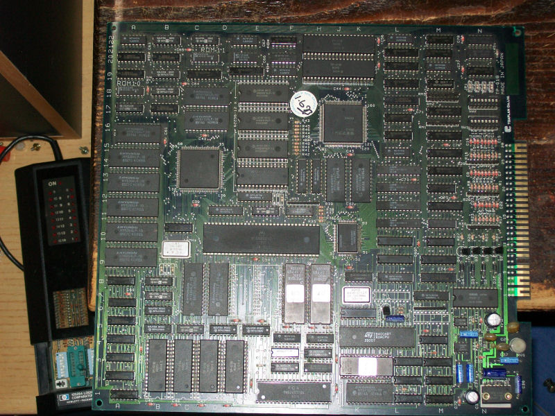
Another faulty board from my friend ‘mastercello’, this time an original Toaplan Out Zone :
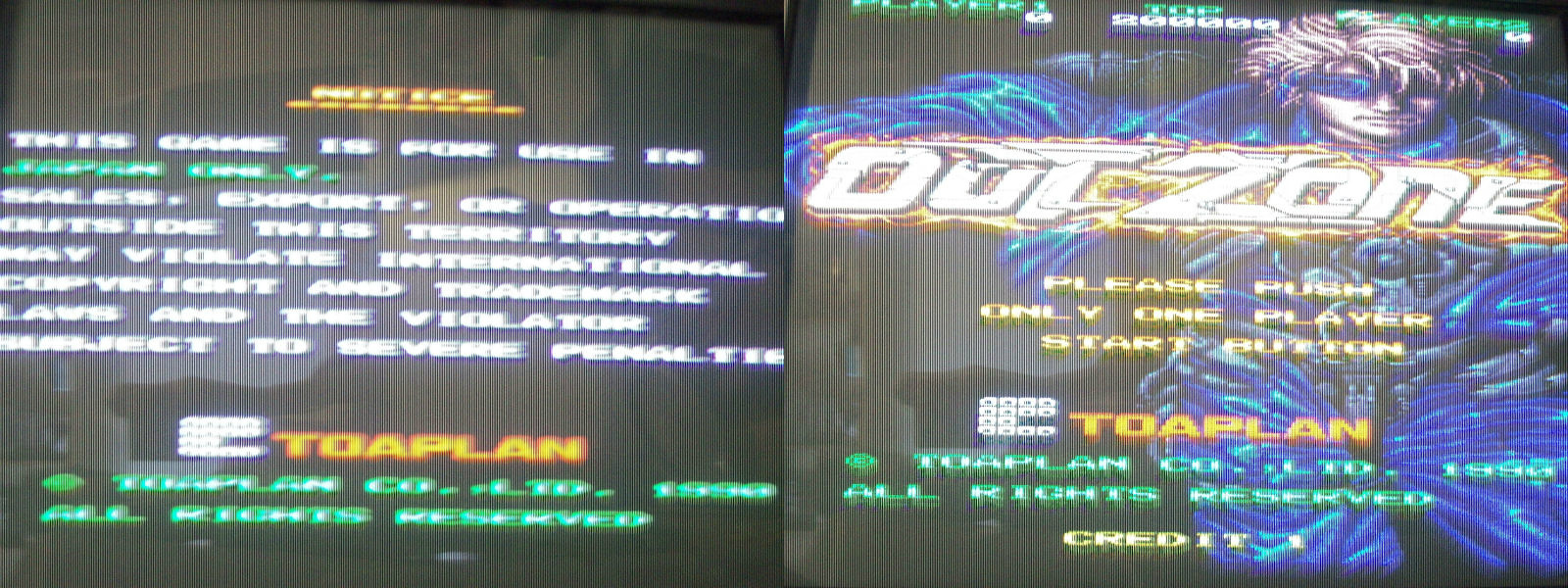
He told me that it worked once and then nothing.Actually when I first powered it up I got this :
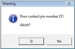
The screen with the wavy lines is common on all the Toaplan PCBs which run on similar hardware.It means that the system is being intialized but it should last until the CPU starts to properly execute code.In my case this screen was permanent so there had to be a problem in the main code execution.First thing I did was to check CLOCK, /RESET and /HALT lines of 68000 main CPU, they were fine.Then I dumped the two 27C010 programs ROMs and got from my programmer a warning about a poor contact on pin 17 (which is a DATA output) of the one labeled ‘TP018_08’:
A closer inspection of the device revealed many oxidixed pins.A bit of fine sandpapering is what the EPROM device needed and enough to fix the board completely.
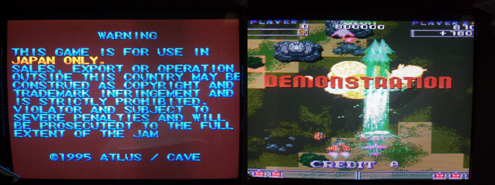
My friend ‘mastercello’ sent me this Donpachi PCB for a repair:
The board was in good shape but had a GFX issue where background layer was partially missing with lines across it:
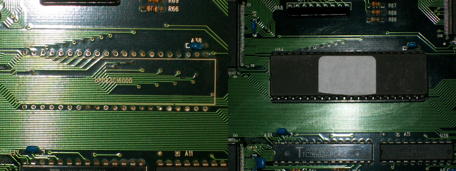
Studying the hardware and with help of MAME I could identify the devices containing the data of the two background layers, they are two 42PIN 8 Mbit MASK ROM @U54 and U57.Probing them with a logic probe I found that the one @U54 has all its data lines stuck LOW or HIGH, also the two control lines /CE and /OE were stuck LOW though they were properly connected to a near ASIC which generates these signals.Obviously this was totally abnormal.As confirmation of my theory I was able to reproduce ths issue in MAME using a dummy ROM file of the background layer data instead of a good one:
This was enough to convince me to desolder the MASK ROM and read it in my programmer resulting in an empty dump.Direct replacement for this 8 Mbit 42PIN MASK ROM is a 27C800 EPROM though the silkscreening under the chip sais ’23C16000′:Fitted a freshly programmed device restored graphics completely.
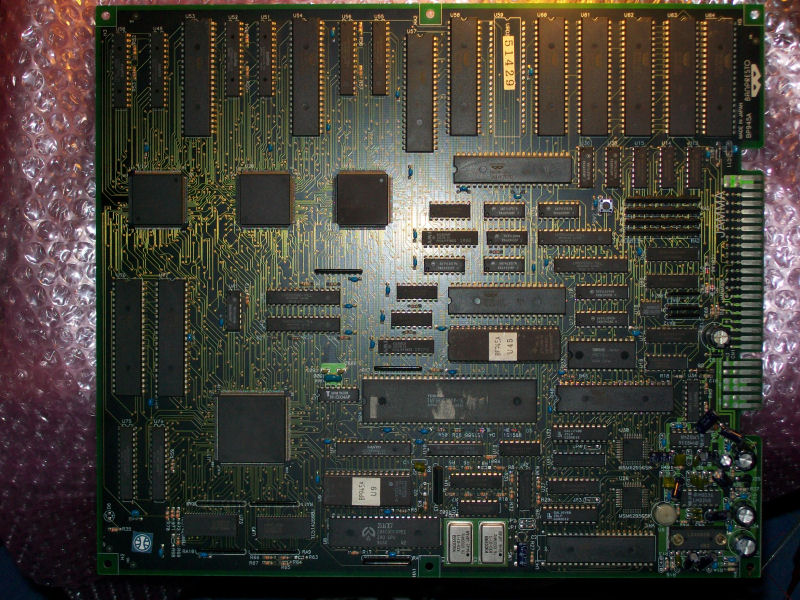
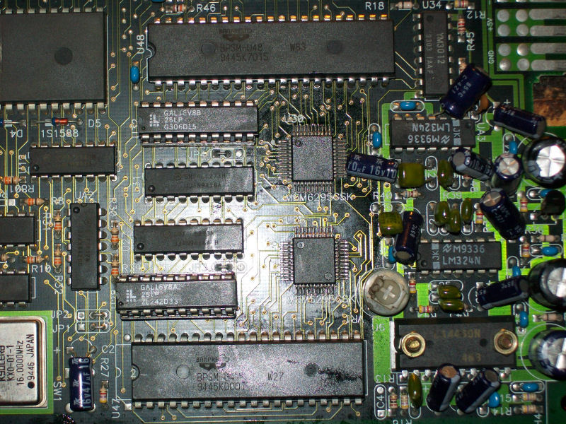
Got this Pretty Soldier Sailor Moon PCB from my friend Ifog:
He told me that gameplay was fine but some of the audio/voice samples were missing or played wrongly.This was confirmed once I fired it up, here’s a brief audio recording:
As beginning of my troubleshooting, for first, I identified the audio digital circuitry:
As you can see from picture above, PCM samples data contained in the two MASK ROMs (40 and 42 pins) are read by two OKI MSM6295 PCM voice synthesis chips (while music is generated by a YM2151).So, I went to probe the MASK ROMs and found that the one @U47 had some address lines stuck as well as the control lines /CE and /OE.
Most of the address lines are directlty connected to the respective OKI MSM6295 chip so I replaced it but with no luck.Instead, I could trace the /CE and /OE lines back to a GAL16V8B @U28.Probing the outputs of this GAL revealed they were all stuck LOW.So. I tried to read it in my EPROM programmer which failed reporting an error:
I also read and disassembled it with my dedicated hardware, it was like empty :
This confirmed definitively that the device was bad.At this point the only possibility was taking a good GAL chip from another PCB or dumping and reproducing it.
Luckily my friend Ifog had a same board with a good GAL and he was able to provide me the binay dump which I took care of analysing and reversing it (see my latest PAL updates here).Once programmed a blank GAL16V8 device and fitted it on PCB, all the PCM samples were restored.Job done.
PAL UpdatesComments Off on Pretty Soldier Sailor Moon PAL dumps added
Jul042015
Today, during a repair (log will follow later) I created the replacements for the two remaining PLDs (two secured GAL16V8B) from a Banpresto Pretty Soldier Sailor Moon PCB.With these two dumps we have now a complete PLDs set of this PCB since the other three (PEEL18CV8 devices) have already been dumped and uploaded on our database though they remain untested.Thanks to Ifog for providing me binary dump of one of the two GALs.
PAL UpdatesComments Off on X-Multiply (IREM M72 hardware) PAL dump added
Jul042015
In the last days I dumped the specific PLD (a PAL16L8) from a X-Multiply PCB (IREM M72 hardware, PAL is on top board ‘M72-C-A’).Chip was kindly provided by my friend ‘robotype’ and dump has been tested as working from ‘cpsystem3’ in a GAL16V8 targeting device.Thanks to both.